= , . ' ,/.." f
HEWLETT-PACKARD CO.
. .11
~
j-T--I-l::i"!
i .• - - - - . _ . _ . . . . c __ •.. _. , .•-t--!pj---;.t
_.1. _.' .••j
NOTE:
This page provides a running history of changes for a mUlti-page
drawing which cannot conveniently be re-issued completely after
each change.
Wh~nmaking a change, list for each page all
before-and-after numbers (within reason; use judgement, and use
"extensive" revision note if loss of past history is tolerable, or
retype complete page) and associate with each a symbol made up of
the change letter and a serial subscript to appear here and on the
page involved (there enc losed in a circle, triangle, or other
attention-getting outline).
Ltr
REVISIONS
DATE
INITIALS
B REVISED PER PCO 52-0844 3-29-85
fJP..JMR
Qf?tS2
6
A
T:Q,s,L
R~k~re-.,
Model No.
I
Stock No. 98626.~66501Title TEST PROCEDURE
Description . Date 3-29-85
By BILL ROBINSON Sheet No. 1 of 12
98626-66501 TEST PROCEDURE
1. TESTS PERFORMED ... 4
2. HOW TESTS ARE DONE ... 4
2.1. Equipment Required ... 4
2.2. Test Setup ... 4
2.3. Running the Test ... 8
3. PREPARING BOARDS FOR SHIPPING ... 1 ~
1. TESTS PERFORl\'1ED
The 98626-66501 board is tested in Product Verification. The only test performed is the bench test (No 3060 testing is done on this board in Product Verification). If a board does not pass the bench test, it is sent to Defect Analysis for repair.
2. HOW TESTS ARE DONE
2.1. Equipment Required
HP Series 9000 Model 226 (9826) or Model 236 (9836) Computer with: HPL ROM Board (98604A) or HPL RAM Disc (98614A)
98256A - 25 6K RAM Memory Board 98620A - DMA Controller Board
9888A Bus Expander (must have hardened backplane1
OPTIONAL - second 988 8A Bus Expander (with ijardened backplane)
ET30106 - HPL Test Disc
ET30117 - Hardened Backplane (in 9888A- Bus Expapder)
98626-67950 - RS232 Test Connector
2.2. Test Setup
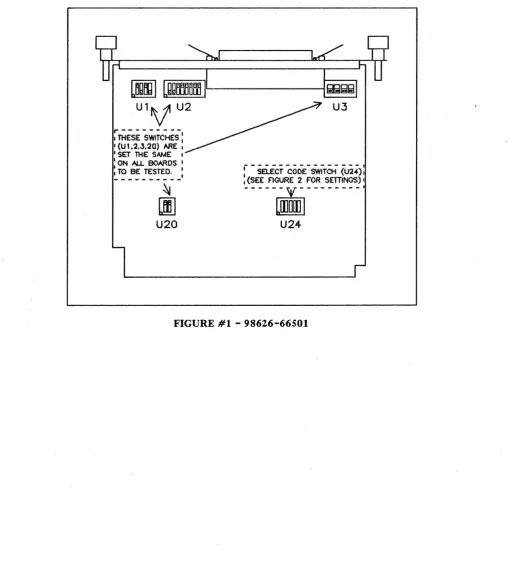
2.2.1. Set U I, U2, U3, and U20 on each of 6 boards to the setting shown in figure 1.
U'V
U2 r---I THESE SWITCHES: I (U1.2.J.2Q) ARE I I SET THE SAME I I ON ALL BOARDS I ~T?_8:
_r:s~:o~_:
~
rml
U20
U3
i-SElECT cODE-SWiTcH (u2i):
: (SEE FlGURE 2 FOR SETTINGS) I
---~---U24
FIGURE #1 - 98626-66501
98626-66501 Test Procedure Drawing A-98626-66501-3
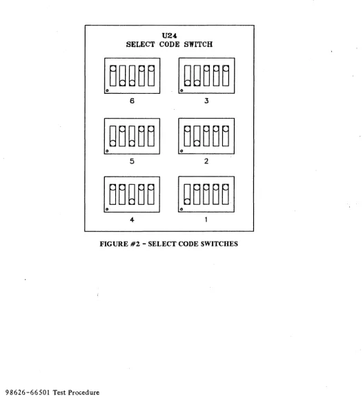
[image:5.619.70.580.135.724.2]2.2.2. Figure 2 shows select code switches (U24) of all six boards being tested. Each board must have its own unique select code. Set the select code switch of board one to I, board two to 2, board three to 3, board four to 4, board five to 5, and board six to 6. (NOTE: The way the select code switches are shown in figure 2 ' l' in the lower right corner and '6' at upper left -also represents how boards to be tested are installed in the 988 8A Bus Expander. See figure 3 and note how the boards are shown in the Bus Expander.)
U24:
SELECT CODE SWITCH
o o
6 3
o o
5 2
o o
[image:6.621.71.597.168.742.2]4
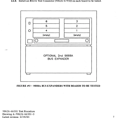
2.2.3. Make sure power to the 9826 Computer and 9888A Bus Expander is OFF. Install boards to be tested in order of their select code (1 through 6), starting on the right side of the Bus Expander. (NOTE: when installing boards into the Bus Expander, make sure to align the boards with the connectors on the backplane and push the boards in using the thumbscrews on the sides of the panel.) A loaded Bus Expander is shown in figure 3.
I
CAUTIONI
BE SURE THE POWER SWITCHES ON THE BUS EXPANDER AND THE COMPUTER ARE OFF WHEN INSTALLING OR REMOVING BOARDS. OTHERWISE, DAMAGE TO BOTH THE COMPUTER AND THE BOARD BEING INSTALLED/REMOVED MAY RESULT.
2.2.4. Install an RS 2 32 Test Connector (9 8626 - 6 7950) on each board to be tested.
0
6 35 2
0
4 1(empty) (empty)
010
I
I
01
I I I
OPTIONAL 2nd 9888A
BUS EXPANDER
L....J L.J
FIGURE #3 -" 9888A BUS EXPANDERS lVITH BOARDS TO BE TESTED
98626-66501 Test Procedure Drawing A-98626-6650 1-3
[image:7.624.68.574.272.772.2]2.3. Running the Test
2.3.1. Insert the disc (ET30106) into the disc drive of the 9826 Computer. (NOTE: A 9836 Computer can be used in place of the 9826 Computer.)
2.3.2. Turn the power switch of the Bus Expander to ON.
2.3.3. Turn the power switch of the 9826 Computer to ON. The test will run automatically and test all boards, one at a time. If all 6 boards pass the bench test, the 9826 Computer)s dis-play will show the following:
::SEVEN I/O CARDS ARE PRESENT:: 98620A:DMA
98626AAT S/C 1 98626A AT S/C 2 98626A AT S/C 3 98626A AT S/C 4 98626A AT S/C 5 98626A AT S/C 6
98626A ON S/C 1 PASSED
98626A ON S/C 2 PASSED
98626A ON S/C 3 PASSED
98626A ON S/C 4 PASSED
98626A ON S/C 5 PASSED
98626A ON S/C 6 PASSED
The names of tests that are run on the boards will be seen at the lower left of the 9826 Computer's display as the test is being performed. If one of the boards being tested does not pass one of the tests, the following is an example of what could be displayed on the 9826 Computer's screen:
98626A ON SIC 2
98626A ON SIC 2 - problem with OCD3/0CD4 outputs
*****
BOARD FAILED*****
Then, either the next board will be tested or, if there are no more boards to test, testing will end. (If you are using the optional second Bus Expander, you can set up six boards in that Bus Expander (see 'Test Setup' section) to run when testing in the current Bus Expander finishes.)
2.3.4. When testing in the current Bus Expander finishes, turn off the 9826 Computer AND 9888A Bus Expander. If an error has occurred on a tested board at a specific select code, tag the board to be repaired with its' error message and date and send it to Defect Analysis.
2.3.5. If you have the optional second 988 8A Bus Expander and it is loaded with boards that are ready to test, turn that Bus Expander on, THEN turn the 9826 Computer on to test these boards. If you are not using the optional second Bus Expander, remove the boards you have just finished testing and set up six more boards to be tested (see 'Test Setup' section) and repeat the process. (NOTE: It does not matter whether you turn off the 9826 Computer or 9888A Bus Expander first, but it does matter how you turn them ON. Make sure you turn on the 988 8A Bus Expander first, THEN turn on the 9826 Computer.)
98626-66501 Test Procedure Drawing A -98626-66501-3
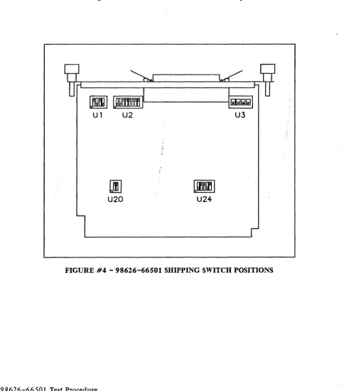
2.3.6. Set switches of boards that pass the Product Verification Test to the shipping switch positions shown in figure 4 (NOTE: The only change is to set the select code switch to the posi-tion shown - which is select code 9).
2.3.7. Stamp the boards that pass the Product Verification Test with the bench test stamp to indicate that they have been tested.
2.3.8. Continue testing until all boards in the workorder are completed.
Ul U2 U3
(jJ
U118rl11
[image:10.624.79.580.197.747.2]U20 U24
3. PREPARING BOARDS FOR SHIPPING
The following steps should be done for each board that passes the Product Verification Test before it is sent to shipping.
3.1. Do an overall visual check of the board including the following: check that components are not lifted from the board; check for components not installed properly - particularly capacitors, resistors, and resistor packs; check for the switches set to their shipping position (see figure 4); . check both sides of the board for excess solder, and close or touching component legs; and, check the painted panel for dirt and scratches.
3.2. Check the date-code of the printed circuit board to make sure it is the right date-code.
3.3. Check each printed circuit board for the bench test stamp.
3.4. Record the serial number of the printed circuit board in the shipping log. (The serial number is located on the white tag on the pad side of the board.)
3.5. Attach the warranty sticker to the pad side of the board, near the serial number tag.
3.6. Clean the gold, male contact-fingers of the printed circuit board with a clean cloth and alcohol.
3.7. Send the board to the shipping area.
98626-66501 Test Procedure Drawing A -98626-66501-3
4. FURTHER DOCUMENTATION
The following list of documentation is included as a reference for those who want more information about testing of this board.
98626 Theory of operation 98626 Schematic
98626 Engineering Ref. Spec. (ERS) 98626 Component Locator
3060 Test Description 3060 Noded Assy. Dwg. 3060 Noded Schematic
Designer's GT 9826 Cardcage DIO Bus Specification
: RS - 232 In terf ace Installation BASIC Interfacing Techniques
ET30106 Description (HPL Test Disc) ET30117 Description (Hard Backplane) 98626-67950 Description
A-98626-66501-9 C-98626-66501-4 A-98626-90300-1 D-98626-66501-5
A-ETI3330-9001-1 C-ETI3330-6001-1 . C-ETI3330-6001-5
A-5955-6551-1 5955-7669 98626-90000 98613-90020
=
=
---=---I
HEWLETT-PACKARD CO.
ItJ.
)'1
NOTE:
This page provides a running history of changes for a mUlti-page
drawing which cannot conveniently be re-issued completely after
each change. When making a change, list for each page all
before-and-after numbers (within reason; use judgement, and use
"extensive" revision note if loss of past history is tolerable, or
retype complete page) and associate with each a symbol made Up of
the change letter and a serial subscript to appear here and on the
page involved (there enclosed in a circle, triangle, or other
attention-getting outline).
Ltr
REVISIONS
DATE
INITIA~SA
As Issued Per PCO 11594
11-9-81
~·JL
..
!
I~.
"~if
~odel No.
98626A
1
Stock No.98626A EXTERNAL REFERENCE SPECIFICATION
• fitleDescription Date
5 October 1981
Bv
Lloyd NELSON
Sheet No.1
of17
~I---H-E-W--L-E-T-T---P-A--C-K-A-R--D--C--O-.--~PJ
________________
~
~~
-.
~
98626A EXTERNAL REFERENCE SPECIFICATION
1.1 SWITCH DESCRIPTIONS
There are five switches on the 98626A interface assembly. These are a select code switch, interrupt level switch, modem status line disconnect switch,
line characteristics switch and a baud rate:select switch. The line charac-teristics and baud rate switches are read at power up/reset and used to determine default values to initialize the UART to.
Refer to Figure I for switch locations and orientations.
Select Code Switch
The setting of this switch determines the base address which the interface will respond to as follows:
Setting Address
00000 600000
00001 610000
.
.
.
1 1 11 1 7FOOOO
Interrupt Level Switch
The setting of this switch determines the level which the interface will interrupt on as follows:'
Sett i n~
ou
0110 11
Interrupt Level
3 4
5
6
Line Characteristics Switch
..
J
lTl
HEWLETT-PACKARD
CO.
tJ.---~
1.2
See
PCModem Status Line Disconnect Switch
03 02 01 00
======================='=====
: R t : DSR : CTS. CD :
============================
This switch is used to disconnect and tie high iriterface receiver inputs connected to unused modem status lines so that they always appear ON. This may be done for one of two reasons. First, crosstalk in a cable can cause spurious interrupts to be generated if the UART is enabled to interrupt on changes of the modem status lines. Second, system. drivers may require that certain modem status lines be ON before transmitting or receiving data and the device on the other end may not drive these lines.
"
Baud Rate Select Switch
This switch is used to select a power up/reset value for the baud rate. Refer to a desc~~ption of register five for details.
CONNECTOR PINOUT
The connector pinout is intended to be compatible with the ALVIN interface and the 2621 terminal so that common cables may be used. The signal and
circuit definitions are for the DTE cable. The OCE cable will map the circuit line so that operation is transparent to the drivers.
Signal f Circuit I Pin II Pin I Circuit; I Signal
oc04 T I 26 OC03
2 I
27
3
r
28
4 I 29
5 J 30
6 I 31 OCR3
7 f 32 TT
8 f. 33
~I
CE
9 I 34+12 10 I 35 +5
-12 11 I 36 +5
Txd BA 12 I 37 SD
RTS CA ··13 II 38 TS
.,. ~-.. ' ,
-OTR CO 14 I I 39 TR
SRTS (OCD2) SCA 15 II 40 CH DRS (OCD1)
16 I I 41
17 II 42 BB Rxd
MODEl 98626A
I
STK. NO.98626A EXTERNAL REFERENCE SPECIFICATION
8' Loyd Nelson DATE 05 October 1981
PQ.1
for Rev; s; 0111-9-81
APPD.·~~ Ci3
OF17 ; C
SHEET NO.-NO APPROVED DATE
HEWLETT-PACKARD CO.
t;.
Signal I C i rcu it I Pin II Pin I Circuit I Signal
SC 18 II 43
19 ft 44 CS CTS
20 II 45 CC DSR
21 I t 46 CF CD
22 II
47
SCF SCD (OCR2)23 I f 48 AS GND
Shie1d 24 II 49
25 II 50
~
HEWLETT-PACKARD
co.
I I. 1 INTERFACE REGISTER MAP AND RESET STATE
==============================================================
MS
o
o
o
o
o
o
==============================================================
RESET INTERFACE ,
.
.
============================================================== ==============================================================
IE IR
._---_._---.
..
.
o
o
INT LVL
============================================================== ==============================================================
.,OCD3 OCD4 OCR2 :OCR3 BAUD RATE SELECT
:---~---~---~---:
o
SCD======~=======================================================
==============================================================
LINE CHARACTERISTICS SWITCH
============================================================== ==============================================================
RECEIVER/TRANSMITTER BUFFER
============================================================== ==============================================================
DIVISOR LATCH LEAST SIGNIFICANT BYTE
============================================================== ==============================================================
MSC I RLSI IREI RBFt
o
o
o
o
:---~---~---:---:o
o
o
o
==============================================================
DIVISOR LATCH MOST SIGNIFICANT BYTE
==============================================================
===================='==========================================
INT 10 INTR
1 READ I WRITE 3 7 17 DLAB=O 17 BLAB=1 19 DLAB=O 19 DLAB=l
o
o
o
o
a
:---~---: 21o
0==============================================================
MODEl 9862 6A STIC. NO.
8626A EXTERNAL REFERENCE SPECIFICATION
DATE 05 October 1981
HEWLETT-PACKARD
co.
tJ.---..
I 1.1 INTERFACE REGISTER MAP AND RESET STATE (cont1d.)
==============================================================
: DLAB : BRK PARITY STB CHAR LENGTH
:---~---~---~---~---;
23
o
o :
o
o
o
o
o
o
============================================================== ==============================================================
Loop SRT DRS RTS DTR :
o
o
o
:---~---~---~---~---:25
o
o
o
o
o :
============================================================== ==============================================================
: TSRE THRE BI FE PE OE DR
o
:---~---~---~---~---~---~---: 27o
o
o
o
o
=================================================.============= ==============================================================
CD R I : DSR CIS :; DCD: TERI :-. ODSR peTS
:---~---~---~---: 29
o :
o
o
o
==============================================================
11.2
07
When the interface is reset, register bits with an underscored lable are set to the state shown. All other labeled bits are either unchanged or
reflect :the current state of the input or switch to which they are connected. A zero or one in an unlabeled box indicates that that bit is always in that state.
REGISTER DESCRIPTIONS
Address 1 READ - 10 Register
06
05
04 03 02 01 00.:===================================================================
MS
o
o
a
o
o
o :
===================================================================
MS - Master/Slave
-HEWLETT-PACKARD
CO.
t;.
Address I WRITE - Control Register
a
07 06 05 04 03 02 01 00
=====================================================================
Reset Interface
=====================================================================
Address 3 READ/WRITE - Interface Interrupt Register
07 06 05 04 03 02 01 00
=====================================================================
IE IR : I NT LEVEL
: SWITCH
x
x
x
x
=====================================================================
IE - Interrupt Enable
Writing a one to this bit enables the interface to interrupt whenever the IR bit is a one.
IR - Interrupt Condition (READ ONLY)
The UART interrupt request line is asserted.
INT LEVEL - Interrupt level switch setting (READ ONLY).
00 - Interrupt 1 eve 1 3
01 - Interrupt level 4
10 - Interrupt level 5
11 - Interrupt leve 1 6
Address 5 READ/WRITE
07 06 05 04 03 02 01 00
======================================================================
BAUD RATE SELECT
: OCD3 : OCD4 : OCR2 : OCR3 : 5
:
:
: (SeD) :
======================================================================
BAUD RATE SELECT SWITCH - (READ ONLY)
These four bits correspond to the setting of the baud rate select switch on the interface. This switch is read by the interface drivers at power up/reset to determine an initial value to initial ize the UART buad rate to as follows:
.,..Ir....t~
___
+---+---t
MODEL 98626AI
STiC NO.~----~---~---4
98626A EXTERNAL REFERENCE SPECIFICATION
Lovd NeJ son DATE 05 October 1981
8V
~ee
Pq.1 For Revision 11-9-81
H EWLETT-PACKA RD
co.
11---Setting Baud Rate
0000 50
0001 75
0010 110
00 11 134 .. 5
01UO 150
0101 j
200 ':;.
0110 300
0111 600
1000 1200
1001 1800
1010 2000
1011 2400
1100 3600
1101 4800
1110 7200
1111 9600
OCR3 - Optional Circuit Receiver 3 (READ ONLY).
This bit returns the current state of the line connected to optional circuit receiver
3.
It is a one when the line is ON and a zero when it is OFF.seD - Secondary Carrier Detect (READ ONLY).
This bit returns the current state of the Secondary Carrier Detect line.
is a one when the line is ON and zero when it is OFF. . ..
OCD4 - Optional Circuit Driver 4. OCD3 - Optional Circuit Driver 3.
Writing a one or zero to these bits turns the corresponding circuit driver It
ON or OFF respectively. These bits can be read to determine the current state of the driver.
Address 7 READ
07 06 05 04 03 02 01 00
===================================================================
LINE CHARACTERISTICS SWITCH: HANDSHAKE : LINE CONTROL REGISTER
: TYPE : INITIALIZATION
===================================================================
LINE CHARACTERISTICS SWITCH
D
HEWLETT-PACKARD
co.
11---.
HANDSHAKE
The setting of these two switches will be used at power up to determine the type of software handshake as follows:
Settin9 Handshake
00 Ack/Eng
01 Xon/Xoff
10 none
10 none
LINE CONTROL REGISTER INIT
The setting of these switches will be used to initialize the UART line control register at power up/reset and will be written into the corresponding bit of that register. See the description of that register for further details.
Addresses 17 - 29 access UART registers.
Address 17 READ (DLAB=O) - UART Receiver Buffer
WRITE (DLAB=O) - UART Transmitter Holding Register
07 06 05 04 03 02 01 00
====================================================================
: :
: :
:
.
====================================================================
The UART receiver and transmitter are both doubly buffered. A character to be transmitted is written into the transmitter holding register. When the trans-mitter shift register becomes empty, the character is automatically transferred to it and shifted out. Another character may then be written into the holding register while the fir~t is being shifted out. Received characters are shifted into the receiver shift register. When this register becomes full, the data is automatically transferred to the receiver buffer where it may be read while another character is shifted in.
Address 17 READ/WRITE (DLAB=l) - Baud Rate Divisor Latch LSByte Address 19 READ/WRITE (DLAB=l) - Baud Rate Divisor Latch MSByte
07
06
05 04 03 02 01 00====================================================================
====================================================================
.~.'-+---~---~---~_MO_D_E_l ___ 9_8_6_26_A ______ ~I~ST_K._N_O_. __________________________ ~
98626A EXTERNAL REFERENCE SPECIFICATION
Loyd N~ 1 son DATE 05 October 1981
See Pq.l for
Revisio~11-9-81
~-t---... .;...;..;,,;;;...-.-;:;....;..;~-...;=r..=...~~___I APPO. SHEET NO. 9 OF 11'-·
lTl PC NO APPROVED DATE
HEWLETT-PACKARD
co.
tJ---.
The uART has an internal Baud Rate Generator. The Baud Rate is set by writing a divisor into the 16 bit divisor latch and is determined by
Baud Rate = 153600/Baud Rate Divisor
To access the Baud Rate Divisor Latch, is is necessary to get the DLAB (Divisor Latch Access) bit of the Line Control register. This will prevent access to the Transmitter Holding register, Receiver Buffer, and the Interrupt Enable register but will allow all other UART registers to be accessed in their normal manner. The DLAB bit should be cleared once the Divisor Latch is initialized.
Address 19 READ/WRITE (DLAB=O) - Interrupt Enable Register
07 06 05 04 03 02 01 00
====================================================================
o
o
o
'0 : MSC I : RLS I : TRE I : RBF I====================================================================
The four LSB of this register enable the UART to interrupt on specific conditions as described below. These bits are set/cleared by writing out a one/zero and are also cleared when the interface is Reset.
RBFI - Enable Receiver Buffer Full Interrupts.
When se~ the UART will interrupt whenever the DR bit of the Line Status register is a one. The interrupt is cleared by reading the receiver buffer or writing a zero to the DR bit of the Line Status register.
TREI - Enable Transmitter Holding Register Empty Interrupts.
When set, the UART will interrupt whenever the THRE bit of the Line Status register is a one. The interrupt is cleared by writing a character into the Transmitter Holding register or by reading the Interrupt Identification register
(if the interrupt was caused by an empty Holding register).
RLSI - Enable Receiver Line Status Interrupts.
When set, the UART will interrupt whenever any of the OE, PE, FE, or BI bits of the Line Status register is a one. These bits and the interrupt can be cleared by reading the Line Status register.
MSCI - Enable Modem Status Change Interrupts.
HEWLETT-PACKARD
co.
1I---.
Address 21 READ - Interrupt Identification Register
07 06 05 04 03 02 01 00
====================================================================
a
o
o
o
o
: INT 10 : INTR====================================================================
INT 10 - Interrupt Cause 10
Indicates the highest priority interrupt currently pending. When the interrupt ID register is read, the highest priority interrupt currently pending is frozen and no other interrupts will be acknowledged until the condition causing the
interrupt is cleared.
INT 10
II
10
01
00
INTERRUPT CAUSE
,Receiver Line Status (highest priority) Receiver Buffer Regist~r Full
Transmitter Holding Register Empty
Modem Line Status change (lowest priority)
Receiver Line Status Interrupt.
A Receiver Line Status interrupt is generated whenever the RLSI bit of the Interrupt Enable register is set and any of the OE, PE, FE, or BI bits of the Line Status register is a one. The interrupt can be cleared by reading the Line Status register which also clears the OE, PE, FE, and BI bits.
Receiver Buffer Full Interrupt.
A Reciever Buffer Full interrupt is generated whenever the RBFI bit of the interrupt enable register is set and DR bit of the Line Status register is a one. The interrupt is cleared by reading the receiver buffer or by writing a zero to the DR bit •.
Transmitter Holding Register Interrupt.
A transmitter holding register empty interrupt is generated whenever the TREI bit of the Interrupt Enable register is set and the THRE bit of the Line Status register is a one. The interrupt i~.cleared by writing into the Transmitter Holding register or by· reading the Interrupt Identification register.
Modem Line Status Change.
A Nodem Line Status Change interrupt is generated whenever the MSCI bit of the Interrupt Enable register is set and any of the ORLS, OCTS, OOSR, or TERI bits of the Modem Line Status register is a one. The interrupt can be cleared by
reading the Modem Line Status register which clears the DRLS, OCTS, ODSR, and TER I bits.
F ' -...
---+---t ...
---t
MODEl 98626AI
STK. NO.~---~~---~ 98626A EXTERNAL REFERENCE SPECIFICATION
IY Loyd Nelspn DATE 05 October 1981
See Pg.l
For Revlslor
11-9-18
HEWLETT-PACKARD
CO.
INTR - Interrupt Pending.
This bit is a zero whenever the UART is requesting an interrupt.
Address 23 - READ/WRITE - Line Control Register
07
06
05 04 02 01 00===================================================================
PAR lTV: DLAB : BRK : STOP : CHAR LENGTH :
: STK : EVEN : PEN :
===================================================================
OLAB - Divisor Latch Access Bit.
When this bit is set to a one, it is possible to access the divisor latches of the Baud Rate generator during a read or write to registers 17 and 19.
BRK - Set Break.
When this bit is set to a one, the TxD line will be forced to the Spacing (logic zero) state and remain there regardless of other transmitter activity. This bit must be cleared to disable the break and reenable normal transmitter activity.
STK - St i ck.
EVEN - Even Parity.
The type of parity that is transmitted or recieved is determined by the setting of these two bits.
Setting
00
01 10
1 },
PEN - Parity Enable.
Pa r i ty
odd par i ty even parity . pa r i t y bit I 1 '
pa r i ty bit I 0 I
When set to a one, this bit enables the transmitter to transmit and the receiver to check for a parity bit between the last bit of the data word and any stop bits. When this bit is set to zero, no parity bit is transmitted or checked.
CHAR LENGTH - Character Length.
The setting of these two bits determines the length of the transmitted and
received characters as follows: :
Setting
00
Bi ts/Char
I
l TI
HEWLETT-PACKARD
co.
11---.
STOP - Stop Bits.
This bit, along with the number of bits/character determines the number of stop bits t ransm it ted after every character.
Setting Bi ts/Cha r Sto~ Bits
0
5,
6,
7,
8 1I 5 I
.5
1 6,
7,
8 2Address 25 READ/WRITE - Modem Control Register
07 06 05 04 03 02 01 00
===================================================================
u
o
o :
Loop : SRTS : DRS : RTS : DTR: : (OCD2) : (OCDI) : :
===================================================================
loop - loopback ..
When set to one, this bit enables a loopback feature for diagnostic testing. The serial output of the UART and therefore TxD are set to the Marking state. The UART receiver input is disconnected and the output of the transmitter shift register is looped back into the receiver shift register. The modem control inputs CTS, DSR, CD, and RI are disconnected externally and connected internally to the four modem control outputs OTR, RTS, DRS, and SRTS.
When in loopback mode, receiver and transmitter interrupts are fully operational. The modem control interrupt source is now the modem control output register bits
instead of the modem control inputs.
DRS - Data Rate Select.
SRTS - Secondary Request to Send. RTS - Request to Send.
DTR - Data Terminal Ready.
Writing out a one or zero to these bits sets the corresponding modem control line ON or OFF respectively. The current state of the lines can be read back.
Address 27 READ/WRITE - Line Status Register
07 06 05 04 03 02 01 00
===================================================================
o
: TSRE : THRE : B I : FE : PE : OE : DR===================================================================
MODEL 98626A
I
STK. NO.98626A EXTERNAL REFERENCE SPECIFICATION
IV Loyd Nel~on DATE 05 October 1981
~ee Pg.l tor KeV1SlO ll-~-~H
~1\
JL_,
APPD "\< .~.~ :-> SHEET NO. 13 OF 17 '
PC NO A"IOVED DATE
HEWLETT-PACKARD
CO.
TSRE - Transmitter Shift Register Empty.
This bit is set to a one whenever the Transmitter Shift register is empty.
Bits 06 - 00 of this register can all be set by writing out a one in addition to the being set by the conditions described below.
THRE - Transmitter Holding Register Empty.
This bit is set to a one whenever the Transmitter Holding register is empty. It is cleared whenever a character is wrftten into the Transmitter Holding register.
BI - Break Indicator.
This bit is set to a one whenever the received data input is held in the spacing condition for longer than a full work transmission time. This bit is cleared whenever the Line Status register is read.
FE - Framing Error.
This bit is set to a one whenever the stop bit after the last data bit or parity bit is at th~ spacing level. This bit is cleared whenever the Line Status
register is read.
P E - Par i t y E r ro r.
This bit is set to a one when the received character does not have the correct even or odd parity as selected by the parity select bit. This bit is cleared whenever the Line Status register is read.
OE - Overrun Error.
This bit is set to a one whenever the Receiver Buffer register was not read before the next character was transferred in from the Receiver Shift register. This bit is cleared whenever the Line Status register is read.
DR - Data Ready_
This bit is set to a dne whenever a character has been transferred into the receiver buffer register. This bit is cleared by reading the receiver buffer register or writing zero to this bit of the Line Status register.
Address 2S READ/WRITE - Modem Status Register
07 06 05
04
03 02 01 00===================================================================
CD , RI DSR : CTS : DCD : TERI : DDSR : DCTS
HEWLETT-PACKARD
co.
tJ---.
RI - Ring Indicator (READ ONLY).
This bit returns the current state of the RI 1 ine., It is a one when the RI 1 ine is ON and zero when it is OFF.
DSR - Data Set Ready (READ ONLY).
This bit returns the current state of the DSR I ine. It is one when the DSR 1 ine is ON and zero when it is OFF.
CTS - Clear to Send (READ ONLY).
This bit returns the current state of the CTS line. It is one when the CTS line is ON and zero when it is OFF.
uCO - Delta Carrier Detect.
This bit is set when the CD line has changed since the last time the Modem Status register was read.
TERI - Trailing Edge of Ring Indicator.
This bit is set whenever the RI line has changed from an ON to an OFF condition.
ODSR - Delta Data Set Ready.
This bit is set whenever the DSR line to has changed since the last reading of the Modem Status register.
OCTS - Delta Clear to Send.
This bit indicates that the CTS 1 ine has changed since the last reading of the Modem Status register.
~'-+---~---+---~~MO_D_E_l_9~:8~6_2_6_A ________ ~I~ST_K._N_o_. __________________________ ~ q8626A EXTERNAL REFERENCE SPECIFICATION
Lovd Nel son DATE 05 October 1981
DATE
Se- Po.1 for Revisior 11-9-81
t--F..;;;...--.-...::..:...t~---.;.;:;..:--.;;:;...;.,;;;~--::;..;;;.-.~;;..;;;..___t APPD. SHEET NO. 15 Of 17 .
PC NO APPROVED
lU
HEWLETT-PACKARD CO.
t;.
Appendix I. Rev. A Register Map.
Address I READ - 10 Register
1 WRITE - Reset Interface
07 06 05 04 03 02 01 00
======================================================.==============
x
x
x
o
o
o
o
o
====================================================================
RS NOP
====================================================================
RS - Reset Interface.
Thfs bit is latched by the interface. I~ is set by writing out a one, at power up, and whenever the Reset line is assert~d. A zero must be written to this bit to clear the reset and enable the interface.
Address 3 READ - Interrupt Status Register.
07
06
05 04 03 02 01 00D
====================================================================
x
IR : I NT LEVELx
x
x
x
====================================================================
IR - Interface is requesting interrupt service.
INT LEVEL - Interrupt -Level switch setting.
00 - Interrupt level 3
01 - Interrupt level 4
10 - Interrupt level 5
11 - Interrupt level 6
Address 5 READ - Switch 2 Setting.
07 06 05 04 03 02 01 00
=======================================================================
HEWLETT-PACKARD
CO.
11---.
Address
7
READ - Switch3 (4
LSB) setting.07 06 05 04 03 02 01 00
====================================================================
x
x
x
X : Swi tch 3 (4 LSB)====================================================================
Reading register
7
returns the setting of the four LSB of switch3.
r
MODEl 98626A
I
STK. NO.98626A EXTERNAL REFERENCE SPECIFICATION
Loyd Ne1s"n DATE 05 OCtober 1981
![Crystal structure of 2 butylsulfanyl 4,6 bis[(E) styryl]pyrimidine](data:image/gif;base64,R0lGODlhAQABAIAAAP///wAAACH5BAEAAAAALAAAAAABAAEAAAICRAEAOw==)