This document w a s prepared under t h e sponsorship of t h e COmmission^ of t h e European Atomic E n e r g y Community N e i t h e r t h e E U E A T O M Commission, i t s contractors n o r a n y person acting on t h e i r behalf :
111
Él^SS.SIlärÉÖ
Make a n y w a r r a n t y o r representation, express o r implied, w i t h respect to t h e accuracy, completeness, or usefulness of t h e
W respect to t h e accuracy, completeness, or usefulness of t h e information contained in t h i s document, or t h a t t h e u s e of a n y information, a p p a r a t u s , method, or process disclosed in t h i s document m a y not infringe privately owned rights ; or
lespecL· LU m e accuracy, completeness, or usetulness of t h e information contained in t h i s document, or t h a t t h e u s e of a n y informat'
documen Assun result: dO(
A s s u m e a n y liability with respect t o t h e use of, o r for damages ï ΟΤΥΊ O
resulting from t h e use of a n y information, apparatus, method or process disclosed in this document.
ι» I '
at t h e price of F F 6.— F B 60.
m'
før
Wr>
www^wWw
mmivmfoiå,
Tins r e p o r t is on sale a t t h e adi addresses listed on cover
DM 4.80 Lit. 750 Fl. 4.30 page 4
; MM
''WM
wïmi
please quote the EUR number and the title, * on the cover of each report.
was reproduced on the basis of the best available copv. P r i n t e d b y L. Vanmelle, s.a. Brussels, A p r i l 1966
y twwtâ töte $
PM
#W ? w P i
ψ
TOfflWíPW
mmmmiÆmMm
EUR 2799.e
DIGITAL COMPARATORS FOR HANDLING OF DATA FROM NUCLEAR EXPERIMENTS by F. COLLING
European Atomic Energy Community — EURATOM Joint Nuclear Research Center
Geel Establishment (Belgium)
Central Bureau for Nuclear Measurements (CBNM) Brussels, April 1966 — 40 Pages — 14 Figures — FB 60.—
Two digital comparators for binary or binary coded decimal inform-ation have been realized and tested. The comparator stages for all bits are cascaded and identical, so that they can be used as standard units in building block systems. The operation time of the 20-bit three-state transistor comparator is about 90 ns per bit for the slowest comparison. With a 10-bit window comparator, containing two two-state
compar-EUR 2799.e
DIGITAL COMPARATORS FOR HANDLING OF DATA FROM NUCLEAR EXPERIMENTS by F. COLLING
European Atomic Energy Community — EURATOM Joint Nuclear Research Center
Geel Establishment (Belgium)
Central Bureau for Nuclear Measurements (CBNM) Brussels, April 1966 — 40 Pages — 14 Figures — FB 60.—
compar-ators with tunneldiodes as threshold elements, a minimum comparison speed of about 6 ns per stage (bit) was reached. This characteristic can be improved up to one order of magnitude, if necessary, when fast tunneldiodes are used.
For data handling purposes two-state comparators should be preferred because of their possible simplicity and speed. A maximum flexibility in application is given, in addition.
Three state comparators, also by combination of two two-state comparators, can be used with advantage for regulation purposes as for instance gain stabilization.
ators with tunneldiodes as threshold elements, a minimum comparison speed of about 6 ns per stage (bit) was reached. This characteristic can be improved up to one order of magnitude, if necessary, when fast tunneldiodes are used.
For data handling purposes two-state comparators should be preferred because of their possible simplicity and speed. A maximum flexibility in application is given, in addition.
EUR 2799.e
EUROPEAN ATOMIC ENERGY COMMUNITY - EURATOM
DIGITAL COMPARATORS FOR HANDLING
OF DATA FROM NUCLEAR EXPERIMENTS
by
F. COLLING
1966
Joint Nuclear Research Center Geel Establishment - Belgium
SUMMARY
Two digital comparators for binary or binary coded decimal inform-ation have been realized and tested. The comparator stages for all bits are cascaded and identical, so that they can be used as standard units in building block systems. The operation time of the 20-bit three-state transistor comparator is about 90 ns per bit for the slowest comparison. With a 10-bit window comparator, containing two two-state compar-ators with tunneldiodes as threshold elements, a minimum comparison speed of about 6 ns per stage (bit) was reached. This characteristic can be improved up to one order of magnitude, if necessary, when fast tunneldiodes are used.
For data handling purposes two-state comparators should be preferred because of their possible simplicity and speed. A maximum flexibility in application is given, in addition.
C O N T E N T S
1 . INTRODUCTION
1.1. Some needs for a digitei comparator in nuclear physics
1.2. Basic function and way of operation of the digital comparator
1.3· Some general aspects of digital comparators
2 . REALIZED COMPARATORS
2 . 1 . I n t r o d u c t o r y c o n s i d e r a t i o n s
2 . 2 . A t h r e e - s t a t e comparator with t r a n s i s t o r s 2 . 2 . 1 . General d e s c r i p t i o n
2 . 2 . 2 . D e t a i l e d d e s c r i p t i o n of t h e c i r c u i t diagram of one s i n g l e comparator s t a g e
2 . 3 · A window comparator c o m p r i s i n g two t w o - s t a t e com-p a r a t o r s with t u n n e l d i o d e s
2 · 3 · 1 · General d e s c r i p t i o n
2 . 3 · 2 . D e t a i l e d d e s c r i p t i o n of t h e c i r c u i t diagram of one s i n g l e comparator s t a g e
2 . 3 · 3 · Tolerance c o n s i d e r a t i o n of t h e c i r c u i t l a y - o u t
3- MEASUREMENTS AND TESTS
3 . 1 . The t i i r e e - s t a t e comparator with t r a n s i s t o r s 3«2. The t w o - s t a t e comparator w i t h tunneldiodes 3*3· I n t e g r a l o p e r a t i o n t e s t
4. CONCLUSIONS
LIST OP PIGURES
L i s t of c i r c u i t symbols
R e a l i z e d c o m p a r a t o r , s i m p l i f i e d b l o c k d i a g r a m . Two c a s c a d e d c o m p a r a t o r s t a g e s «
T h r e e s t a t e c o m p a r a t o r w i t h t r a n s i s t o r , b l o c k d i a g r a m .
T h r e e s t a t e t r a n s i s t o r c o m p a r a t o r , one com p a r a t o r s t a g e «
T h r e e s t a t e t r a n s i s t o r c o m p a r a t o r i n M.L.
mode; £ v s . m f o r K, » K » K.
* max l 2
Threestate transistor comparator in M.L.
mode; m vs. n for K, » L·.
Threestate transistor comparator in L.M. mode; £ vs. m for K, « K~ « K.
* max l c.
Threestate transistor comparator in L.M. mode; m vs. n for K, =■ K.
General b l o c k d i a g r a m of t h e window c o m p a r a t o r , The t i m e diagram of t h e window c o m p a r a t o r . T w o s t a t e t u n n e l d i o d e c o m p a r a t o r , one compa r a t o r s t a g e .
I n t e g r a l o p e r a t i o n t e s t , b l o c k d i a g r a m . T w o s t a t e c o m p a r a t o r w i t h t r a n s i s t o r * , one c o m p a r a t o r s t a g e .
[image:8.595.84.515.93.686.2]P i g . 14 T w o s t a t e c o m p a r a t o r w i t h t r a n s i s t o r ^ vs. n.
Table I Threestate comparator in M.L. mode, possible comparison c o n d i t i o n s of t h e s t a g e " S " .
Table I I T w o s t a t e c o m p a r a t o r i n L.M. mode, p o s s i b l e comparison c o n d i t i o n s of t h e s t a g e " S " .
P i g .
P i g .
P i g .
P i g .
P i g .
P i g .
P i g .
P i g .
P i g .
P i g .
P i g .
5
-1. INTRODUCTION (o)
1.1. §ome_needs_for_a_digital_çom2ajator_in_nuclear_p_hjsicsi
The analog signals from particle detectors will mostly be digitized in analog-to-digital converters. The further handling of the experiment information will therefore be done in a digital manner.
In order to attain adequate resolution, many bits will be required. Especially in multiparameter experiments, which are of increasing importance » the data words will be extremely long. As a consequence, big store
capaci-ties will be required. If such big stores are not available, one has to look for a compromise between the desired resolution, experiment time and instru-mentation capabilities.
It will often happen, that only a smaller part of all channels (data words) are of real interest. If one could provide the physicist with a unit, which would permit the selection of one or more regions of interest, either the quantity of information or the number of bits per data word - to be stored - could be reduced.
A digital comparator is a unit which enables the selec-tion of a region of interest. It will discriminate whether the information has a greater value than a selected number, or a smaller one. Two comparators combined to one unit will enable the user to select a window. In this manner, the quantity of information to be stored and handled may be reduced to a certain amount.
Comparators can also be used for the integration of selected parts of the spectrum. Besides a reduced quantity of information, one will also get a smaller number of bits at the cost of a decrease in resolution for that particular parameter, of which the parts are selected. In certain cases a unit with subtracting
properties should be used for the selection of a region of interest.
Maintaining the same resolution with a reduced number of bits would be the main advantage. To obtain a di-gital window, an additional comparator would be re-quired. Particularly for experiments with on-line analysis, it can be of real advantage - or even a requirement - to have the disposal of a unit which allows a reduction of the number of bits per word. Por off-line experiments,on the other hand, a unit which reduces the quantity of information words to be stored, may also be useful.
It may be pointed out, that the application of a digital comparator will not by far be limited to the above mentioned goals. Besides the use as a selector of regions of interest, there will be other appli-cations for data processing.
1.2. Basic_function_and_way_of_op_eration_of_the_digital comparator.
A digital comparator compares a digital data word (number X) to a digital programmed word (number A) and indicates whether the number X is greater than A, smaller than A, or equals,A.
Generally, all available data words are compared with one programmed word during one data handling cycle. In some applications it may occur that one data word
is compared to several programmed words. , In most cases, the number of stages of the comparator
will at least be equal to the number of bits of the programmed word.
The comparison is effectuated as follows:
Each comparator stage compares the corresponding bits of A and X. Some stages detect equality of the
conclusion of the comparison must be prescribed by the stage of highest significance of all stages de tecting unequality.
1.3. Some 2βηβΓ^1_Β3^βοΐ8_οΐ_^1^ΐ§1_οο5ρ_ΒΤ^θΓβ.
Two- and three-state comparators have been realized for the comparison of digitized data.
A three-state comparator (1,2,4,5,6) is able to iden tify separately if a data word (X) is greater, equal or smaller than a programmed word (A).
In a two-state comparator (3,7J, two of the three possible states are combined to one state and X > A
or X < A, X < A or X > A, X / A or X * A, can be
identified. A unit with the latter mentioned property is known as an equality detector and is normally very simple in lay-out.
In most of the known comparators, the comparison pro cess begins with a separate comparison of bits with the same significance. Concerning the detailed com parison procedure, i.e. in principle how to find out the most significant bit for which unequality is given and the way to elaborate the result, different solutions have been described (] - 6).
In general a comparator should allow a symmetrical access of digital numbers to be compared. Special comparator types, in which the programmed word can be controlled only manually by means of mechanical switches or
relays, are better characterized as digital thresholds (1,3). They are not very flexible in application, but can be very simple in lay-out.
In nuclear experiments, comparators have been used by different people, to reduce single parameters in
8
-is fixed by the programmed words of two single com-parators.
Por the planned applications, which are more general, comparators should allow a high degree of flexibility. Needing only one comparator stage per data word bit seems to be the most suitable solution. The comparator stages are then identical for all bits, so that they
can be used as standard units in a building block system. An improved version of such a proposal (6), which is a
three-state comparator allowing automatic programming, if needed, has been realized by us and will be desribed. Another solution (7), a two-state comparator for which the same concept was applied, but simpler in lay-out and allowing greater processing speed,has been deve-loped in addition. It is this latter type of comparator which meets our demands in the best way.
2. REALIZED COMPARATORS
2.1. Introductor^_considerations
Both realized comparators - a three-state comparator with transistors and a window comparator, consisting of two identical tvo-state comparators with tunnel-diodes - comprise n similar cascaded stages (Pig. 1). The number of stages n is not limited for circuitry reasons; both the required quantity of components and comparison time are roughly proportional to the number of bits (n).
The following description is related to Pig. 1. Each stage compares a bit of the dava word (X) with the corresponding bit of the programmed word (A). Both words are supposed to be binary or binary decimal coded. The comparison result of one stage is determined either by the information delivered from the preceding stage, or by the configuration of the two applied bits.
The symbols x., a. and c. reeprésent the configuration -th
9
-"i"~ comparator stage; χ and an represent the most
significant, χ and a the least significant bits of X and A.
The result of the comparison of A and X may be available at the output of that comparator stage, corresponding either to the most or to the least significant bit (C or C ). The latter is possible, if the most sig nificant comparator stage detecting unequality will impose its result to all comparing units between that deciding stage and the output.
If the comparator output is at the most significant stage, the flow of decisive information will be from less significant stages to the most significant one
(L.M. mode). The deciding comparator stage imposes then its result to more significant comparator stages, which all must have detected equality.
If the output of the comparator is at the least signi ficant comparator stage, the flow of deciding infor mation will go from a more significant to the least significant stage (M.L. mode). In this case the de ciding comparator stage must impose its result to less significant comparator stages, which may have detected themselves unequality of both sign»or equality.
In case both words A and X are equal, the single com parator stages do not influence each other; every stage produces an equality signal.
10
will need about the same time, if the comparisons are
initiated by clock pulses, because the fastest allowed repetition rate is given by the comoarison needing the longest time to be effectuated.
The functional analysis of a comparator can be reduced
to the examination of two consecutive stages R and S (Pig.2")
The signal R . is the comparison result of the stage R, provided that the stage preceding it does not influence
the comparison of H(Q . ■ 0)· The symbols X, Xg and Ap, A« represent the information delivered by two conse
cutive bits of the data word (X) and the programmed word (A). The comparison result of the two examined stages, S . , is determined by the analog sum of the three input
signals delivered to the stage S (E 4.» X« BIͱ Ag) .
According to the significance of the stage R, either the unequality signal R . eliminates the influence of any
configuration of Xg and Ag (M.L. mode), or R , is
eliminated by an unequality signal produced by Xg and A„ (L.M. mode). As either unequality decision (X > A or
X < A) can be caused by different combinations of the
three input signals, their analog sum can reach different
values, but the output signal must attain always a dis crete level for the same decision. This can be reali zed by the introduction of a threshold device, delivering the
required output level, if the sum of the input signals is greater than the threshold. The weight of the three input signals R_ut» Ag and Xg must be chosen in such a
way that for either unequality between A and X, their sum has the right value in relation to the threshold.
A threestate comparator stage needs two opposite thres holds. If neither threshold is reached, the comparator
indicates equality of A and X.
A twostate comparing unit has only one threshold. The
- 11
-a driving sign-al sm-aller th-an the threshold, where-as for the opposite unequality case the sum of input signals must be greater than the threshold.
A three-state comparator can be realized also by
an adequate combination of two two-state comparators.
2.2. Three-state comparator with transistors
2.2.1. General descri/Dtion
A three-state comparator has been built as a general study for the comparison of binary or binary coded -decimal information with up to 20 bit word length. All comparator stages are equal and contain two
transistors as main elements. The realized comparator is identical in principle to a circuit given
by others (6) but it requires only two supply voltages (+ 6 V), which are in use as standard vol-tages for digital electronic equipment in our
laboratories.
The required input signals and the delivered output signals are of the same "level"-type: a binary "one", "1" = + 5 V and a binary "zero", "0" » 0 V.
A data word (X) to be compared with the programmed word (A) is stored via read-in gates in a 20 bit binary register (Pig. 3). A buffer stage is used between the register and the comparator, allowing
a greater fan-out for the connection of different comparators.
The programmed word can be controlled manually by means of twenty toggle switches, which allow to
connect the MA" inputs of the comparator stages to
a voltage of 0 Volts or - 4,3 Volts^respectively.
12
-power supply voltage of - 6 Volts with zener diodes. On the circuit cards of the comparator, space was provided for an A- register and a suitable coupling
stage, to allow an electronic control of the pro-grammed word.
The three different comparison resiilts X > A, X = A, X < A are available at seperate outputs; for instan-ce for "X > A", the voltage at the "X > A" output is: Uq » + 5 V and Ug = 0 at the other outputs.
The course of a comparison process can be explained with Pig. 3· An incoming clock pulse will first reset the X-register via an input logic unit. Then the
X-word to be compared which is available at "read-in", is stored into the X-register via read-in gates
with a "set" pulse. The "set" pulse has a fixed delay with respect to the "reset". After setting, the com-parison begins and its result will be available for the realized comnarator at the output of the least significant comparator stage (M.L. mode"). The time necessary for a comparison depends on the words to be compared and on their number of bits. The maximum nossible comparison time determines the delay between the clock pulse and a strobe pulse, which will sense the output logic unit in such a way, that the state of tùileast significant comparator stage is directed
13
account by using the complements of the corresponding
bits for the comparison in the even numbered stages.
2.2.2. Eescrip^ion_of_a_single_com^
The l a y o u t of one s t a g e (S) preceded and followed
by i d e n t i c a l s t a g e s (R and T) i s shown i n P i g . 4«
The s t a g e R i s connected to a more s i g n i f i c a n t b i t
of t h e words to be compared (R a? C. .) and Τ to a
l e s s s i g n i f i c a n t b i t than S (Τ
Η C . _/. ) .The comparison
r e s u l t i s a v a i l a b l e a t the comparator stage b e
longing to the l e a s t s i g n i f i c a n t b i t (M.L. mode).
The t h r e e s t a t e s of t h e comparator s t a g e r e p r e s e n t i n g
the d i f f e r e n t p o s s i b l e r e s u l t s X > A, X » A,
X
-e
A are r e a l i z e d by using two complementary
t r a n s i s t o r s as a d i f f e r e n t i a l switch.
Por an uneqiiality between X and A, e i t h e r t r a n s i s t o r
must be switched on, while the o t h e r one i s in the
c u t o f f s t a t e . In the given c i r c u i t and for X > A,
the i n p u t s i g n a l S^r must exceed a p o s i t i v e t h r e s
hold v o l t a g e , S^r > tUu' to switch on the npn
t r a n s i s t o r ( T . ) . The corresponding output s i g n a l
(S
. ) i s of n e g a t i v e p o l a r i t y , beca\ise of the phase
i n v e r s i o n in t h e t r a n s i s t o r s which are used in emit
tergrounded c o n f i g u r a t i o n . Por X
<
A, S^ has to
overcome a n e g a t i v e t h r e s h o l d v o l t a g e , |Syj,
T|> U»,^,
to switch on T~ and S , will be p o s i t i v e . For
¿
out
x
e q u a l i t y between X and A, both t r a n s i s t o r s w i l l be
in t h e c u t o f f s t a t e , | S™)
<
+ Νψττ· The output
s i g n a l of the unloaded stag«
1will be z e r o , because
of t h e symmetrical l a y o u t of t h e c i r c u i t .
- ik
-Xg * Ujg, if the "i»~th bit (x. ) of the data word is
in the "1" state; Uyg is a positive voltage, equal
for all comparator stages and it may be written: Xg + 1 (X"s » 0) for x± "1", Xg 0 (îg + 1)
for x. 0«
4~ Vi
Ag Η ü.ß, if the " iM~ bit of the programmed word
^a.1 is in the "1" state and a negative signal will be delivered to the comparator stage S. U.g is a
negative voltage and it follows: Ag » 1 (Xg » 0) for & i n1 " ; Ag 0 (Ig = 1) for a± 0.
The signal R . fwhich is delivered by the preceding
stage R, represents the comparison result of the more significant stages. If also here unity signals are taken for an easier explanation, R_utis a positive
signal for X >A, i.e. RQ U t + 1 ; RQ u t 1 if
X < A and R . 0, if X =. A. out
If the necessary predominant influence of R . o n the comparison r e s u l t , for R . y£ 0, i s taken into consideration, one may write for the analog sum of input signals, which should determine S ^ :
SIN « Z'Rout + XS + AS ( 1 )
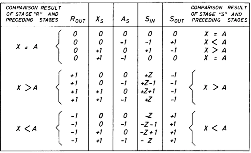
R , , Xg and Ag are unity signals as stated before and ft i s a factor, Ζ > 1#
In table I , the nossible comparison conditions for the stage S are given. Two most c r i t i c a l conditions for a correct operation of the comparator can be defined with the results for S™ in table I .
IN
The predominance condition; if the result of the
preceding stages (Ri .) is opposite with respect
to the result of the stage S itself, R . must
have the greatest weight in order to determine the
state of the stage S; for (X > A)f i and Xg <Ag or
15
The independence condition; if Ro u^ 0 and Xg ¿ Ag,
the signal Xg respectively Ag must not be influenced
by the zero signal level delivered from the prece
ding stage R to the input of S, Xg or Ag have to
determine the state of the stage S.
Por the layout of a comparator stage, the quantita
tive behaviour of a transistor as threshold device must be taken into account. In case of an unequality
decision, the threshold voltage TT__ must not only be exceeded; the transistor which is to be saturated
will also draw a current I, because of its limited π
current gain (8). The current, which is necessary to
bring the transistor into the "on" state, will be: bmin *** B B / P . R and the corresponding overdrive
factor is Κ = I,/I·. . . Por reliable operation and
b nmin '
sufficient speed of response, a minimum overdrive factor K . > 1 should be assured and the minimum ρ
m m
of the used transistors has to be taken into account. However, the overdrive factor Κ will also influence the minimum time interval between two comparisons in
another way. The greater K/o, the greater will be the baseemitter junction charge to be discharged in case of a change in the comparison state of a stage i.e.
the minimum distance between two different comparisons increases with increasing K/P.
The maximum overdrive factor Κ will occur, if the m
same unequality for consecutive bits is given. I SjjJ *» Z+1 and the greatest value of Κ will depend on the maximum
m
current gain of the used transistors. The smallest pos
sible value of the ratio Κ/Κ_. for this circuit can be found bv calculations. (K /K . ^ 5 for R^R > 0t5 ) .
m min 17 c —
16
The smallest value of K is given for the before men
tioned most critical comparison conditions. Por the
■predominance condition one obtains:
fm 2 (m + 1)
•[m (1 + 5Π
6 + 2 g
K1 =
U,
(2)
U,
h
RB*S
*S
with m » y I n g ; ? jr c — J
C C DO DO
U
T H
and c = vy
' ï
UBB
and for the independence condition it is found:
5 2 c
2 c
K,
· [
2 ' n 1 + m
( 3)
K. and Kp have a minimum for 8 «
p min *
t>
and ρ of equations (2) and (3) are determined by
the supply v o l t a g e c o n d i t i o n s . Λ i s smaller than one,
because buffer s t a g e s are used between t h e r e g i s t e r
and t h e comparator. Best d r i v i n g c o n d i t i o n s can be
achieved with K,. » K. = K. An overdrive f a c t o r of
Κ .
a 2 seems to be n e c e s s a r y for a r e l i a b l e o p e r a t i o n .
The maximum allowed value of
κ
can be c a l c u l a t e d i n
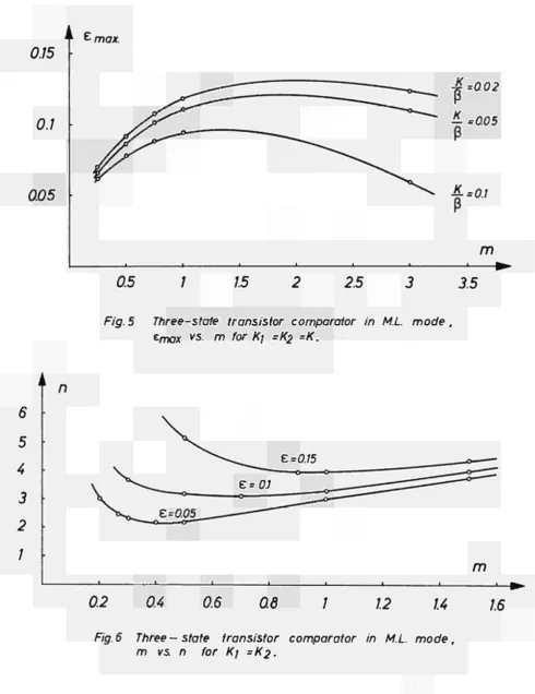
function of m with K/p as parameter. (Pig» 5 ) · As shown,
the maximum value of e t h a t can be t o l e r a t e d
depends
only to a l i m i t e d e x t e n t on 8 for which a minimum
value, guaranteed by the t r a n s i s t o r manufacturers, must
be c o n s i d e r e d . The v a l u e s of m and η should be kept
as small as p o s s i b l e , in order t o o b t a i n high o p e r a t i o n
speed. The b e s t values for m with
Έ/ρ
» 0,1 are
0,5 < m <- 2 for which
r.
v a r i e s between 0,08 and
— — max
0,095· The corresponding values of η can be c a l c u l a t e d
with equation ( 4 ) , which follows from (2) and (3)
(Pig. 6 ) :
o 1 + m
n
"
2 5·
Ü (4)
17
-Por the used silicon transistors and the standard power supplies (U-Q-D » + 6V) a value of c smaller than e , was realized by using as threshold
vol-UISLA.
tage the difference between the base-emitter saturation voltage and the diffusion voltage of biased germanium diodes in the emitters of the tran
sistor pairs.
Por a comparator, designed for operation in L.M. mode, ε can be greater,as shown in Pig. 7· The best values for m are: 1 < m ^ 3 with 0,14 < e < 0,15, (5-20 and Κ — 2. The corresponding values for η are given in Pig. 8.
A greater value of t _ admits either smaller supply max
voltages - of interest for the realization of a com parator with integrated circuits - or greater threshold voltages U ^ .
The collector current of the saturated transistor can be chosen in a way to obtain maximum switching speed. The collector resistor is then fixed for a given supply voltage (RQ » BB/I-) and Rg and RD are determined
by the factors η and m.
With the chosen circuit lay-out (Pig. 4) it was not necessary to select transistors. Reliable operation, also for the critical comparison conditions, was reached within a great temperature range because the threshold voltages of the comparator stages are lar gely independent on temperature. This is due to the mutual compensation of the temperature coefficients
of the transistor base-emitter voltage and the diffusion voltage of the biasing diode.
2.3» A window comparator comprising two two-state compara tors with tunneldiodes.
2.3.1. 2S5eral_descrigtion
18
-t w o - s -t a -t e compara-tors of -ten s-tages each.
The data word (X) and both programmed words (A, and
Ap) are stored in 10-bit binary r e g i s t e r s .
If the window boundaries should be c o n t r o l l e d only
manually, the A - r e g i s t e r s can be replaced by tum
b l e r s r e p r e s e n t i n g the two signal l e v e l s c o r r e s
ponding to the s t a t e s of a binary b i t .
Both two-state comparators w i l l t e s t whether X > A,
( r e s p . Ag) or I < A, ( r e s p . Ag)· The lower
(resp.
upper) l i m i t of the window i s represented by A,
( r e s p . Ap). The decisions of these comparators
are
fed to a logic u n i t , which w i l l d e l i v e r a signal at
only one of the t h r e e outputs, l a b e l l e d
nX > Ap
n,
"A-L
<
X < A
2" and " I
<
Α
χΜ.
All the required input s i g n a l s and the delivered o u t
put s i g n a l s are of the same
l ,level
M-type :
W
1
Mκ* + 5 Volt; "0" M 0 Volt and the used power
supplies are i n accordance with the
ESONS
r u l e s
( +6 Volts and -6 Volts ) .
The time needed for merely the evaluation of one
10-bit data word i s smaller than 60 nanoseconds. The
maximum comparison r a t e for the r e a l i z e d u n i t i s limited
to 5· 10 words per second, because some a d d i t i o n a l
time will be required for other purposes, as for
instance the r e a d - i n of data.
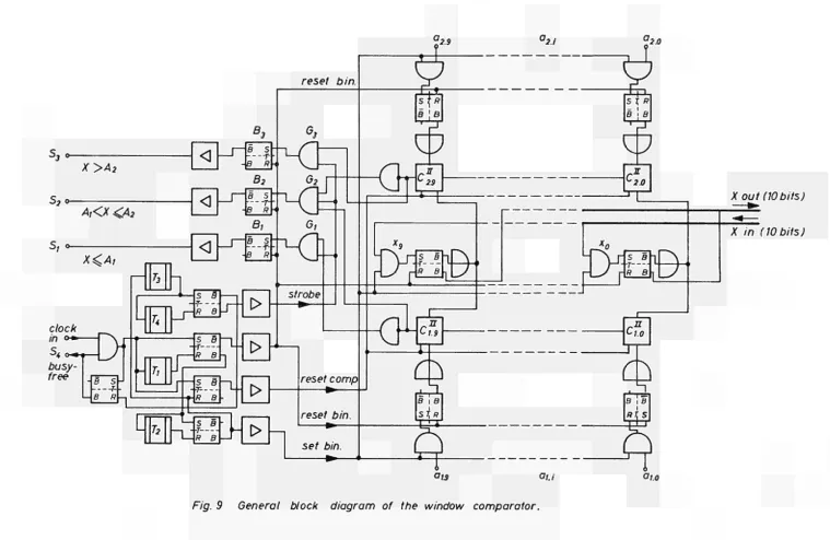
The block diagram of the r e a l i z e d window-comparator
i s shown in
Pig.
9· The time diagram for the different
s i g n a l s during one comparison cycle i s represented
in P i g . 10» The following d e s c r i p t i o n i s r e l a t e d to
both f i g u r e s .
19
closed and the "busy"signal appears at i t s output (S¿,); at the same time the r e g i s t e r s , both comparators and the three output binaries (B, , B~ and B,i will be reset. After a time T, the numbers X, A, and Ap are readin into the appropriate registers by means of a common setpulse. After (T, + Tp) the reset signal to both comparators will be removed, i . e . the actual comparison i s started. Within 60 ns a com parison result will be available, preparing only one of the three output andgates (G, , Gp or G_). Then the strobe pulse passing the prepared andgate vail set the appropriate output binary (Β, , Bp or B,^. The clock input gate will be opened again and the "busyfree" level will turn to "free". Until the next clock signal i s given, the windowcomparator conclusion ( i . e . either X > Ap or A, <· X < Ap or X < A,) will remain available at the corresponding output (either S, , Sp or S).
2.3.2. Description of the_circuit diagram of one_single çqm p_arator_stage
The circuit of a twostate comparator stage with a tunneldiode as threshold element i s shown in Pig. 11. According to the bistable behaviour of a tunneldiode, the reset position can be characterized with a
binary value "0", for which the low voltage state should be prefered in our case. Thus "reset" binary "0", means U ^ < U ^ and "set" binary " 1 " ,
means UmT> > U , -. . Because of the low r e s i s t i v i t y
TD val 1 ey "
- 20
a set stage will return under such conditions to the low voltage state, due to a lack of current, a bias current IM > Iy is supplied to each stage.
As it can be seen from the circuit diagram (Pig. 11), the current through the tunnel diode will be deter-mined by the three possible input signals, i.e. on one hand X« and Ag from the corresponding X- and
A-bits and on the other the signal RQ114-i delivered by
the preceding stage (R). The significance of these three signals must be determined in accordance to the working principle of the comparator. If the
stage S detects unequality, it will be set (S . - "1") for Xg > Ag; for Xg < A« the stage will remain in
the reset position (S . - "O"). S . has the value "1" only for X > A, because the realized comparator is of the "X > A" type. According to the L.M.-mode of operation of this comparator, a signal from the preceding less significant stage (fiout) may only
contribute to the comparison result of the stage S, if the stage S detects equality.
Summarizing the above mentioned conditions :
S . must be "1", independent of H ,. S . must be "0", independent of ROU4-.
S . can be determined by K t·
With table II it is shown that the given comparison conditions can be fulfilled if the X-bit and the complement of the A-bit (X) are fed to the two bit-inputs of each stage.^Por an "X < A" type comparator, X and A should have been applied.) This necessity follows from the fact that a comparison is equivalent to a simplified subtraction. It is to be performed, for an X > A comparator, by adding to the minuend (X) the complement of the subtrahend (X) and the eventual carry pulse from a preceding less significant stage
P o r P o r P o r
XS > AS
Xg < Ag
21
(R . ) . The sum will be greater "1", i.e. a carry signal (S t » "1") is produced, only if at least
two of the three possible signals are present. The sum itself is neglected.
The given conditions for digital signals must be
transformed into analog input currents ibr the tunnel diode. With the symbols in Pig. 11 one may write:
U U. U
τ X . τ A . τ O
x
x
"
ζ
;h
SJ »
XRout ■ SC ·
U is the mean voltage difference between a set and o
a reset tunnel diode. The signals should be chosen
equal to allow maximum tolerances for the elements
of the comparator, i.e., Iy I. I po u t ■ Ig. (6)
The already mentioned biasing current Iw (L·, > Iy) and the signal current Ig can be determined in re
lation to the peak current (Ip) of the tunnel diode. The tunnel diode must not be set if one input current
Ig is delivered, i.e.:
hi
* h <
τν;
(7>
on the other hand, the tunnel diode must be set if
at least two signals Ig are present, i.e.:
hi ** XS » *p · ( 8 )
In order t o allow maximum t o l e r a n c e s for Ig and I ,
one should s e l e c t t h e maximum n o t r i g g e r s i g n a l
( I « + I g ) and t h e minimum t r i g g e r s i g n a l (Ijj + 2 Ig) symmetrical to t h e peak c u r r e n t . I t t h e r e f o r e follows from e q u a t i o n s (7) and ( 8 ) :
h -
(IM
+V -
(IM
+ 2V -
Xp
or
I . - I (I - I M ) . (9)
"S
f <s
- v.
Por the selected tunnel diode (AEÏ 11, I » 5mA ♦ 5%)
-
zz
-Iy = I
p/ 6 ,
I
A= l p / 4
(10)
and for I
gwicn (9) and ^10)
Ια =
UZ
01)
"S
■ν
For tne used tunnel diode one finds: 1M = 1.25 mA,
M
Ig = 2.5 mA.
A reset current Impa is required, before a new com
parison can oegin. T m s current must be greater than
zae
maximum possiuie tunnel diode current, i.e.:
IBES
> 2 JS
+hi
5 Λ I
p0 2 )
For safety reasons it was chosen, Iggs
s^ 5 I« »
BB/
m2.3.3· ?2iÊ£§S2Ë_£2üËèüË£§5i25Ë_°ï_5iiÈ_!ii££Hè5_i
ayr2
uÈ
The allowed tolerances for the signals of a comparator
stage and its elements follow from the critical com
parison conditions mentioned above and were analyzed
for a stage S.
For a maximum notrigger signal, (I„ + Ig
) , the tunnel
diode should remain in the reset state. Such con
ditions are given for the stage S if : Xg < A~,
XTJ > Aη and the stage preceding R also in the set
position. The signal Iao u t = Ig delivered to the stage
S, will have its maximum value for a maximum U of
7
o
the stage R because of element tolerances. Worst
case conditions may occur if in addition, the peak
current of the tunneldiode in the stage S will be
lower than its mean value.
A minimum trigger signal (1^ + 2I
g) to set the stage
S, is given for Xg = Ag, X
R> A
Rand the stage
23
the mean value because of the load condition of R. Worst case conditions may be given if the peak cur rent of the tunneldiode in stage S is higher than
its mean value and U , , of the stage R has its minimum value because of element tolerances.
If the set stage S (Xg > Ag) has to deliver tvro
signals Ig to its neighbouring stages R and Τ
(Xg < Ag, Xm A«) the tunnel dinde of stage S could be reset because of overload if I„ is smaller than
Iy. However,this is improbable because the time necessary to switch a tunneldiode to the high vol tage state is shorter than the switching time for
the inverse direction. As soon as the tunneldiode of Τ has reached the high voltage state, the stage S has
to deliver only one signal Ig.
The tolerances of the used elements are:
I = 5mA + 5% ; 1_ . Ζ < 2,10 /·σ
p " Ì * t ~
Γ
17p, =* 4?C TCV + 1 0 %\ * UP £ 2 irV/0C
A t
(U a tunneldiode forward voltage for I™. = 1^)·
The resistance tolerances are giv<=n with + 5 %·, and
variations of the "set" voltage U were smaller than
+ 15 % for the possible load conditions of a stage.
Calculations have shown, that for a supply voltage
variation of + 1 % and an ambient temperature between
+ 10 °C and + 40 #C, the safety distances of the
signals from I , , 25 % under ideal conditions, are
peak'
reduced to 6 % of I .
Ρ
3. Measurements and tests
ZH-di seussod worst case comparison conZH-ditions and the
maximum comparison time were measured. An integral operation test controlling the faultless working of both comparators for temperature and supply vol
tage variations, was carried out by determining the maximum comparison rate. The maximum clock rate will be lower to a certain extent because of the
limited speed of the associated electronic circuitry for logic operations.
3.1. The threestate_transistor_comparator
To control the critical comparisons, the minimum overdrive factors for the predominance and the in
dependence comparison conditions (Κ,, Σ«) were determined by measuring the corresponding base cur rents in all comparator stages. The lowest values
of K/p which were found are:
B1 ~ Λ ,,£ . 2 B2 ~ « „3.
c c
i.e. for the minimum current gain, Ρ min ■ 20, it follows:
Klmin = 5 and K ^ = 2,5
The maximum overdrive factor (X ) , which occurs when m
two consecutive stages have detected the same un equality, can also be determined from the maximum measurable base current,
m = bm = 0,66
c
i.e. for ñ = 100, Κ = 6 6 .
max ' max
25
-being detected on all stages, and the next decision gives equality of all compared words. The time
interval from the begin of such a comparison (X - A) up to the moment at which the result is available
at the comparator output was % 8 us, i.e. about 90 ns per stage.
3. 2. The_two2State_turjieldiode_comp_arator.
On both two-state comparators of the window compa rator, the same tests were performed separately. Por the critical comparison conditions, mentioned under 2.3*3·, the minimum differences between the tunneldiode current (Inm) and the tunneldiode peak current were measured for all stages.
The security margin of ImD· which avoids a forbid
den setting of a tunneldiode, was found to be
(Ln-In,-) » 6r TD min ρ % of I . The minimum excess current to set a tunneldiode was found to be (Iom~Ip)min "7 %
of Ip.
A too important undershoot of the reset pulse could have introduced an erratic setting of a stage. Por the realized comparator, the undershoot was not greater than 3 % of I v. Therefore a correct
pe aK
operation also under worst case conditions could be assured.
3· 3· Integral operation test.
Both comparators were tested under identical operational conditions. An enual probability for all possible data words in one test interval was reali zed by using the data word register as a
scaler (Pig. 12"), i.e. in one scaler cycle all data words (0-¿ ~ ) occured only once. Por a complete test of the comparators, * test cycles would have been necessary to compare all possible programmed words with all data words. However, the manually con-trolled programmed words were set in such a way
that the correct operation of the critical compa-rison conditions of each comparator stage could be checked in n+1 tests.
Special care was taken to measure only during com-plete scaler cycles,and with an auxiliary scaler,
the number of cycles in one test interval could be fixed.
Por temperatures between 20 and 45*0 and power sup-ply variations of + 1 %, the maximum comparison rate ·. for which the comparator still delivered faultless results was measured. The minimum inter-val between two consecutive comparisons is given by the sum of the maximum comparison time and the time needed for the detection of the comparison result. The number of the HX > A" results per scaler
cycle is given by the programmed word.
~ 27
-The minimum i n t e r v a l between two comparisons, within
the f a u l t l e s s operation range, was measured with
1
#9 tjs for the t r a n s i s t o r comparator and 100 ns for
■che tunneldiode solution. I t was p r a c t i c a l l y indepen
dent on the above indicated temperature and power
supply v a r i a t i o n s . The t r a n s i t i o n from the f a u l t l e s s
into the faulty operation region was sharp, in the
order of one or several percents of the maximum
comparison r a t e for the t r a n s i s t o r or the tunnel
diode comparator^respectively. The measuring accuracy
was 10" .
4.
Conclusions
The i d e n t i c a l layout of a l l stages for the realized
comparators, allowing t h e i r application as flexible
u n i t s in a building block system, has been proven
as a very useful feature.
Por data processing applications, where mostly d i g i t a l
thresholds are needed, twostate comparators are
to be prefered. to t h r e e s t a t e comparators. A two
s t a t e comparison can be characterized as a more fun
damental logic operation and therefore twostate com
parators are in general more flexible in application
and in addition simpler in layout. Por t h r e e s t a t e
comparisons an adequate combination of two twostate
comparators can be used without appreciable additional
element needs.
Threestate comparators are neces
sary for regulation purposes, as for instance the
s t a b i l i z a t i o n of gain by using d i g i t a l references .
The realized twostate comparator uses stow tunnel
diodes as threshold elements. Paster tunneldiodes
would allow an increase in operation speed up to
an order of magnitude
fif necessary.
28
-elements i s t h e i r b i s t a b l e c h a r a c t e r . Short
un-desired signal t r a n s i e n t s , l i k e the undershoot
of the r e s e t s i g n a l , have to be kept small.
If great operation speed i s not needed, a t r a n s i s t o r
can be used as threshold element also for a
two-8 t a t e comparator. The c i r c u i t lay-out of one stage
and the q u a n t i t a t i v e design considerations are
given in Pig. 13 and P i g . 1 4 , r e s p e c t i v e l y .
Acknowledgements
29
-Literature
(1) Y. Amram, H. Guillon, J. Thenard, Oonf. on Nucl.
Electr. II, 85 (Belgrade 1961).
(2) I.N. Hooton, AERE Harwell, Report R3402 (1960).
(3) M.G. Strauss, Nucl. Instr. & Meth. 29, 69 (1964).
(4) C.H. Vincent, Nucl. Instr. & Meth. 29, 306 (1964).
(5) H. Weinstein, Ι.E.E.E. Transact, on Electr. Comp.,
EC-12, 410 (1963).
D-
Ί>
AND INVERTER EMITTER
Β
FOLLOWER
- R B S Β B -FLIP-FLOP BINARY
-E-AMPUFER DIGITAL
DELAY
Θ
.m
TWO STATE THREE STATE COMPARATOR COMPARA TOR STAGE STAGE
- f t
DISCRIMINATOR SCALER
χ*
c„
α„
χη-1
c
n.,
On-t
x¡
Ol
Χι
c,
ot
Χο
Co
Οο
Fig.1 Realized comparator, simplified blockdiagram
"I Qout
J
R
T
Rout
i
F
Souί Γ"
clock
i
setreset
ii
¡i
input logic unit
*I9 *16 read-in
ν
srt R
Β j Β
ST R
I
e j Θ
η
b 1
Xu.m
Ί9
.m
78f
Al9
i^/β
i o i o
i
S T R
1
VXo
-ΠΓ
~JAo
\ 1 o
output logic unit
-o Χ >A -o X =A
-o X <A
strobe pulse
-o read out
Rp=Rc=6õ0n ; RB=W6 ; RD=390Sl; T, = 2N706 ; T2 ΞFW413B; D = 0A&5.
χ = " / " , C/x = +4.Jl/ σ = " 7 " , OU =-4.JV
χ = " 0 " , Ux= OV a = "0"tUA= OV
i ε
max.0.15 ■
0.1
0.05
4=0.02
Ζ- =0.05
β
4-=0.1
β
m
[image:38.595.62.553.87.724.2]0.5
1.5
2.5
3.5
Fig. 5 Three-state transistor comparator in Ml. mode,
emox vs- m for Kf =K2 =K.
Π
6
5
4
3
2
1
m
0.2
0.4
0.6
06
1
1.2
1.4
1.6
■max. ί =0.025
0.2
0.15
0.1
005
m
0.5
1.5
25
35
Fig. 7 Three - state transistor comparator in L.M. mode t
'max vs. m for Κ j =K2 =K
2.5
1.5
0.5
m
0.5
1
1.5
2.5
ST R Β ! fl
2.0
LS riff B\\J
X out (10bits)
X in (10 bils)
[image:40.842.42.801.58.552.2]Oio
Π
-. 7 "
Τ\ ' t.
π ^
~~Ί
_ - . - "
q^L
1 δ κ« 1 ιJW///A-1
ι
ι
ι
C/OCÄ busy freereset binaries set binaries reset comparator strobe pulse
maximum comparison time
Fig.10 The time diagram of the window comparator
oUxR [R=C"
*o
Ux<
Η
31"°"
¡
¿UAR
ROUT #S\
Te
+^ee
1
lA=C/
'."FT!r α
ΤΜ
„
//?f
ï
15 OUT
. J
'neu'']
ι
^"s
π I
,,
1—' - UBB (RESET)
R„ = 3K9 ; RB= 1KB ; RD = I50ÍI
1
UÃTχ = Ί" , Ux=+4.3V; x=V' ,Ux = OV
α = Ί" , UÃ=OV ; α='Ό" ,UÃ=*4.3V
TD=AEY 11
start
s Β τ—
\R _8.
pulse gen.
ST R
I
a ! β
stop
ST R
|B Ι Β
™
-Η
C η C
J.
J
oOn an-i ao
Fig.12 Integral operation test ; blockdiagram.
to counter
oUxR Uxc
- " e s i ^ s f l î
Ts-C/"
x = "7" . ÜXM+43V ;
σ = " 7 " , 6ÎÎ-- O l ' , σ ^ ' Ό " , i/ä =*<J y
/ι Jfn δ;
χ = Ό " , £/*= 0
0.2
0.15
0.1
0.05
Ρ
= 0.024-=0.05
4-=ο.ι
Ρ
η
1
2
3
4
.
COMPARISON RESUL Τ OF STAGE "R" AND PRECEDING STAGES
X = A <
χ y A <
X <A < / \ / \ / \ ROUT 0 0 0 0 + 1 + 1 + 1 + 1
_ J —1 -1 Xs 0 0 +1 *1 0 0 + 1 +1 0 0 +1 +1 As 0 -7 0 -1 0 -1 0 -1 0 -1 0 -1 S/N 0 -1 +1 0
*z
*Z-1 +Z+1*z
-z
-Z-1 -Z*1- ζ
SQUT 0 +1 -1 0 -1 -1 -1 -1 +1 +1 +1 +7
COMPARISON RESULT
OF STAGE " S " AND PRECEDING STAGES
X = A X < A
x y
AX = A <
< /
x y
Ak /
[image:44.595.105.505.90.334.2]X < A \
Table I Three- state comparator in M. L. mode .
Possible comparison conditions of the stage 'S ".
COMPARISON RESULT OF STAGE "R-AND
PRECEDING STAGES ROUT
Χζ.Α <
xyA <
r
o
0 0
l o
{ 1
1 1 Xs 0 0 7 7 0 0 1 1 As 0 1 0 1 0 1 0 1 Ãs 1 0 1 0 1 0 1 0 SUM 7 0 0 7 0 1 1 0
COMPARISON RESULT OF STAGE "S" AND
SoUT PRECEDING STAGES
(CARRY)
0 X < 4
0 Χ ζ,Α
ι
x y
A0 X < 4
7 xy A
0 Χ ζ.Α
ι
x y
Aι
xy
ATable II Two-state comparator in L.M. mode .
[image:44.595.90.523.475.650.2]ippi
mm
■ < 1 ί
»lÍÍíÍ
!:ji' ' ::;;ΐ::
^lllllllllUilillïUlllllllliilÜtll To disseminate knowledge is to disseminate prosperity — I mean - general prosperity and not individual riches — and with prosperity disappears the greater part of the evil which is our heritage from
SALES OFFICES
AH Euratom reports are on sale at the offices listed below, at the prices given on the back of the cover (when ordering, specify clearly the EUR number and the title of the report, which are shown on the cover).
PRESSES ACADEMIQUES EUROPEENNES
98, Chaussée de Charleroi, Bruxelles 6
Banque de la Société Générale Bruxelles compte N° 964.558,
Banque Belgo Congolaise Bruxelles compte N° 2444.141,
Compte chèque postal Bruxelles N° 167.37,
Belgian American Bank and Trust Company New York compte No. 22.186,
Lloyds Bank (Europe) Ltd. 10 Moorgate, London E.C.2, Postcheckkonto Köln Nr. 160.861.
o
υ
>o
to <ι ^o W OOFFICE CENTRAL DE VENTE DES PUBLICATIONS DES COMMUNAUTES EUROPÉENNES
2, place de Metz, Luxembourg (Compte chèque postal N° 19190)
BELGIQUE — BELGIË
MONITEUR BELGE
4042, rue de Louvain Bruxelles BELGISCH STAATSBLAD Le.uvenseweg 4042 Brussel
GRAND-DUCHE DE LUXEMBOURG
OFFICE CENTRAL DE VENTE DES PUBLICATIONS DES COMMUNAUTES EUROPEENNES 9, rue Goethe Luxembourg
DEUTSCHLAND
BUNDESANZEIGER Postfach Köln 1
FRANCE
SERVICE DE VENTE EN FRANCE DES PUBLICATIONS DES
COMMUNAUTES EUROPEENNES 26, rue Desaix Paris 15e
ITALIA
LIBRERIA DELLO STATO Piazza G. Verdi, 10 Roma
NEDERLAND
STA ATSDRU KKERIJ
Christoffel Pianti]nstraat Den Haag
EURATOM —