© 2016, IRJET | Impact Factor value: 4.45 | ISO 9001:2008 Certified Journal
| Page 135
AMBA-AXI Protocol Verification by using System Verilog
G.Kanaka Maha Lakshmi
1, M. Manasa Lakshmi
21
Student, Department of ECE, Gandhiji Institute Of Science and Technology, Andhra Pradesh, India
2
Assistant Professor, Department of ECE, Gandhiji Institute Of Science and Technology, Andhra Pradesh, India
---***---Abstract -
This paper mainly focuses on verifying the important features of advanced extensible interface (AXI). Verifying the memory transactions of AX I includes the verification of all the five channels write address, write data, write response, read address and read data. In this work a Verification Intellectual Property cores (VIP) based methodology is used to carry out the verification Process. In the VIP design the entire test environment is modeled using system verilog and the read, write transactions from the same and different memory locations has been verified with the quantitative values of Busy Count, Valid Count and its Bus Utilization. Verifying the System connectivity during write and read cycles is also one of the fundamental features verified in this paper.
Key Words
:
Write and Read transactions, AXI
protocol,Verification IP, Bus utilization, Coverage
mode analysis.
1.INTRODUCTION
The Advanced Microcontroller Bus Architecture (AMBA) is a protocol that is used as an open standard; on-chip interconnects specification for the connection and management of functional blocks in a system-on-chip (SoC). The AMBA bus is applied easily to small scale SoCs. Therefore, the AMBA bus has been the representative of the SOC market though the bus efficiency. Three distinct buses are defined within the AMBA specification:
1. Advanced Peripheral Bus (APB). 2. Advanced High performance Bus (AHB). 3. Advanced extensible Interface Bus (AXI).
The AMBA specification defines all the signals, transfer modes, structural configuration, and other bus protocol details for the APB, AHB, and AXI buses. The AMBA APB is used for interface to any peripherals which are low bandwidth and do not require the high performance of a pipelined bus interface. APB peripherals can be integrated easily into any design flow, with the following specification:
• Peripheral bus for low-speed devices • Synchronous, non multiplexed bus • Single master (bridge)
• 8, 16, 32-bit data bus • 32-bit address bus
• Non-pipelined
AMBA AHB is a new level of bus which sits above the APB and implements the features required for high performance, high clock frequency systems, with the following specification:
• Burst transfers • Split transactions
• Single cycle bus master handover • Single clock edge operation
• Wider data bus configurations (64/128 bits)
AXI extends the AHB bus with advanced features to support the next generation of high performance SoC designs. The goals of the AXI bus protocol include supporting high frequency operation without using complex bridges, flexibility in meeting the interface, and performance requirements of a diverse set of components, and backward compatibility with AMBA AHB and APB interfaces. The features of the AXI protocol are:
• Separate address/control and data phases • Support for unaligned data transfers
• Ability to issue multiple outstanding addresses • Out-of-order transaction completion.
2. PROPOSED WORK
The work is proposed in this project is the achievement of communication between one master and one slave using Verilog, then verifying the design using System Verilog.
2.1 Design of AXI Protocol
© 2016, IRJET | Impact Factor value: 4.45 | ISO 9001:2008 Certified Journal
| Page 136
Fig -1: Block Diagram of a system
In AXI protocol, every transfer is done using hand shake mechanism. Each channel uses the same VALID/READY handshake to transfer control and data information. This two-way flow control mechanism enables both the master and slave to control the rate at which the data and control information moves. The source generates the VALID signal to indicate when the data or control information is available. The destination generates the READY signal to indicate that it accepts the data or control information. Transfer occurs only when both the VALID and READY signals are HIGH. There must be no combinatorial paths between input and output signals on both master and slave interfaces.
2.2 Address Write Channel (AW Channel)
[image:2.595.39.283.101.266.2]AXI_MASTER drives the write command signals only when ARESETn is HIGH, else it drives all signals as zero. The address write command signals driven by the AXI_MASTER are - AWID,AWADDR, AWBURST, AWLEN, AWSIZE, AWCACHE, AWLOCK, AWPROT, with AWVALID as HIGH indicating that the driven signals are valid. The AXI_MASTER does not drive the AWVALID signal as LOW, until it receives the AWREADY signal, which is driven by the DESTINATION_SLAVE, indicating that, it has received the address write command signals. If AWREADY is LOW, then AXI_MASTER retains the same values. Fig-2 shows the state diagram for the address write command signals.
Fig -2: State diagram of Address Write Channel
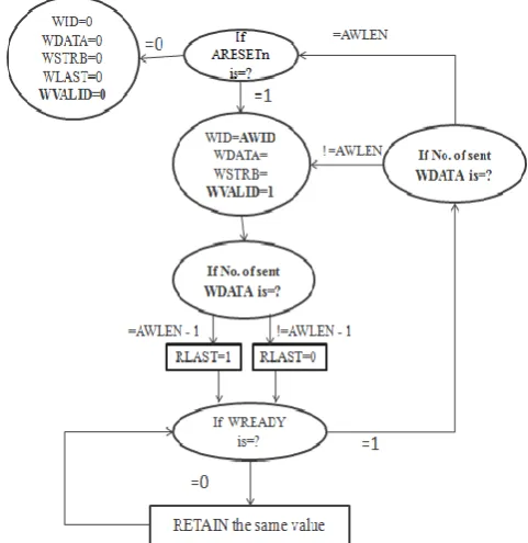
2.3 Write Data Channel (W Channel)
The AXI MASTER drives these Write Data signals, after sending the write address command signals. It drives these signals, only when ARESETn is HIGH, otherwise it drives all signals to zero. AXI MASTER drives the WDATA signal with WVALID as HIGH, it holds the same value until it receives the WREADY signal. If WREADY is HIGH, it drives the next WDATA. AXI MASTER drives the AWLEN No. of data. While driving the last data it drives the WLAST as HIGH. Fig-3 shows the state diagram for the WRITE DATA channels.
[image:2.595.309.550.498.746.2]© 2016, IRJET | Impact Factor value: 4.45 | ISO 9001:2008 Certified Journal
| Page 137
2.4 Write Response Channel (B Channel)
The DESTINATION_SLAVE drives these Write Response signals, only when ARESETn is HIGH, otherwise it drives all signals as zero. DESTINATION_SLAVE waits for WLAST signal. After receiving the WLAST signal, it drives these response signals, with BVALID as HIGH. It holds the same value until it receives the BREADY signal from the AXI MASTER. If BREADY is HIGH, it drives all the signals as zero, at next positive edge of ACLK, otherwise it retains the same value.
2.5 Address Read Channel (AR Channel)
AXI_MASTER drives the command signals only when ARESETn is HIGH, else it drives all signals as zero. The address read command signals driven by the AXI_MASTER are - ARID, ARADDR, ARBURST, ARLEN, ARSIZE, ARCACHE, ARLOCK, ARPROT, with ARVALID as HIGH indicating that the driven signals are valid. The AXI_MASTER does not drive the ARVALID signal as LOW, until it receives the ARREADY signal, which is driven by the SOURCE_SLAVE, indicating that, it has received the address read command signals. If ARREADY is LOW, then AXI_MASTER retains the same values
2.6 Read Data Channel (R Channel)
The SOURCE_SLAVE drives these Read Data signals after receiving the read command signals. It drives these signals, only when ARESETn is HIGH, otherwise it drives all signals as zero. SOURCE_SLAVE drives the RDATA signal with RVALID as HIGH, it holds the same value until it receives the RREADY signal. If RREADY is HIGH, it drives the next RDATA. SOURCE_SLAVE drives the ARLEN No. of data. While driving the last data it drives the RLAST as HIGH.
3.VERIFICATION ENVIRONMENT
The entire verification environment for verifying the AXI transactions is shown in the Fig-4. It consists of a generator module to read the test cases to satisfy the criteria's of verification. In this paper we focus primarily two different
test scenarios verifying the read and write transactions in same address and different address locations. The two test cases are driven to bus functional model with mailbox as a synchronization medium. Bus functional model plays a vital role in receiving the generated transactions and drive them to the AXI interface. The verification environment is developed using system verilog and it can be reconfigurable to any Device under Verification (DUV) according to the verification plans and strategies. Nowadays the verification environment is coming as inbuilt verifying option with all System on Chip (SOC's) so called as Verification Intellectual Property (VIP).
Fig-4 VIP for verifying memory transactions
4. RESULTS AND DISCUSSIONS
4.1Verification of write architecture
© 2016, IRJET | Impact Factor value: 4.45 | ISO 9001:2008 Certified Journal
| Page 138
acknowledgement will takes place. Similarly the write response will happen at the high state of BVALID and BREADY signals. Here the signal AWLEN is of four bit size [0:3] which generates different transactions from one to sixteen. During that generation process if AWLEN is 0100 then it will have 0101 transactions which mean it will increments the transactions by one. This is clearly illustrated in the waveform clearly at Fig-5. From the waveform it is observed that AWSIZE indicates the size of each transaction. The entire write architecture is simulated and verified for all the signal toggle counts which is clearly show in the waveform in Figure-5
Fig-5 AXI Write Cycle Response.
The signals verified in this test case are AWADDR, AWVALID, AWREADY, and WDATA along with their write address, write data’s signals. Also the signals WLAST, WVALID, WREADY, BRESP, BVALID and BREADY are also verified for every transactions. The parameters VALID COUNT, BUSY COUNT, BUS UTILIZATION are calculated practically with this test case and the bus utilization is shown in percentage numbers. Write phase is divided into three channels response. The necessity to verify write phase is whether hand shaking of signals is happening perfectly or not in all the three channels.
VALID COUNT for read phase = 13. BUSY COUNT for read phase = 16.
BUS UTILIZATION = (13/16)*100 = 81.25 percent
4.2Verification of write architecture
In this read cycle verififcation, all the read architecture signals ARVALID, ARREADY, RVALID, RREADY, RLAST, RDATA and ARSIZE are verfified for each transcations. The read architecture includes two channels i.e. read address and read response channels. The read address channel will intialize its address fetching at the high state of ARVALID and ARREADY signals for every positive edge of global clock. Similarly after a gap period of delay read response will instantiated to high mode for every positive edge of RVALID and RREADY signals. RLAST indicates the last transaction in the RDATA signal. Similarly ARSIZE and ARLEN are same as compared to that of write architecture. The entire waveform for the verififcation satge of the read architure is given Fig-6.
Fig-6 AXI read Cycle Response.
© 2016, IRJET | Impact Factor value: 4.45 | ISO 9001:2008 Certified Journal
| Page 139
hand shaking of signals for each channel then only a proper read phase will happen.
VALID COUNT for read phase = 10. BUSY COUNT for read phase = 13.
BUS UTILIZATION = (10/13)*100 = 76.92 percent. The same read and write phase is verified using the code coverage mode analysis and the coverage driven report is given in the Fig-9. The code coverage mode analysis is covering about the 80% of verification IP using the random test bench based verification methodology. The sample coverage report for the AXI Slave/Master for the various analyses like state machine, branches, transitions and toggle counts etc., is given below as follows
Table-1
: Bus utilization for different phases
Different Phases Bus Utilization
1 Read Phase 76.92%
2 Write Phase 81.25%
3 Write and Read
Different location
66.25%
4 Write and Read
from Same loaction
95.45%
From the Table - 1 it is inferred that the bus utilization percentage is 76.92% and 81.25% for the individual read and write phase respectively. In the same manner the bus utilization for the combined read and write in the same and different memory location will be of 66.25% and 95.45% respectively.
Fig-7:Coverage mode analysis
© 2016, IRJET | Impact Factor value: 4.45 | ISO 9001:2008 Certified Journal
| Page 140
5. CONCLUSION
The AXI protocol verification, and the signals used in each channel are verified and analyzed using the code coverage mode analysis. The main advantage of this kind of verification is using the pseudo random coverage driven verification, where the time to market is less and applicable for complex designs using system verilog verification. In future we develop a test case to verify both the write and read phase simultaneously from the same location and different locations of read and write.
ACKNOWLEDGEMENT
I express my sincere gratitude to Mrs. M. Manasa Lakshmi, Department of ECE Studies, GIST college, India and also thanks to for continuous guidance and other Professors of Department of VLSI Design and Embedded Systems, GIST, India for extending their help & support in giving technical ideas about the paper without which I would not come up with this paper
REFERENCES:
[I] K. Swaminathan , G. Lakshmi narayanan a, Seok·Bum Ko "Design and verification of an efficient WISHBONE·based network interface for network on chip". Computers and Electrical Engineering 40 (2014) 1838-1857
[2] S. Saponara a, L. Fanucci a, M. Coppola "Design and coverage·driven verification of a novel network· interface IP macro cell for network·on· chip interconnects". Microprocessors and Microsystems 35 (2011) 579- 592 [3] Alan P. Su, JifT Kuo, Kuen·Jong Lee, Ing·Jer Huang, Guo·An Jian" A Multi·core Software/Hardware Co·debug Platform with ARM CoreSightTM, On·chip Test Architecture and AXIIAHB Bus Monitor ".
[4] Attia B, Zitouni A, Tourki R. Design and implementation of network interface compatible OCP for packet based NOC. In: International conference on design & technology of integrated systems in nanoscale era; 2010. p. 1-8.
[5] Technical Reference Manual of Prime Cell AXI Configurable Interconnect (PL300), ARM, Cambridge, u.K., 2010.
[6] Singh Sanjay Pratap, Bhoj Shilpa, Balasubramanian Dheera, Nagda Tanvi, Bhatia Dinesh, Balsara Poras. "Generic
network interfaces for plug and play NoC based architecture ". In: Lecture notes in computer
science Springer reconfigurable computing: architectures and
applications; 2006. p. 287-98.
[7] Chien·Hung Chen, .Jiun·Cheng .Iu, and Ing·.Ier Huang, "A Synthesizable AXI Protocol Checker for Soc Integration ", IEEE transl, ISOCC, Vol 8,pp.I03·106, 2010
[8] Lai Yong·Long, Yang Shyue·Wen, Sheu Ming·Hwa, Hwang Yin· Tsung, Tang Hui·Yu, Huang Pin·Zhang. A high· speed network interface design for packet·based NoC. In: IEEE ICCCAS; 2006. p. 2667-71.
[9] .I. Shao and B. T. Davis, "A burst scheduling access reordering mechanism, "in Proc. IEEE 13th Int. Symp. High Perform. Comput. Archit.,Feb. 2007, pp. 285-294.
[10] Fattah M, Manian A, Rahimi A, Mohammadi S. "A high throughput low power FIFO used for GALS NoC buffers". In: IEEE annual symposium on VLSI; 2010. pp. 333-8.