www.arpnjournals.com
PARITY BASED FAULT DETECTION TECHNIQUES FOR S-BOX/ INV S-BOX
ADVANCED ENCRYPTION SYSTEM
Nabihah Ahmad
Department of Electronic Engineering, Faculty of Electrical and Electronic Engineering, Universiti Tun Hussein Onn Malaysia (UTHM), 86400 Parit Raja, Batu Pahat, Johor, Malaysia
E-Mail: [email protected]
ABSTRACT
Concurrent fault detection plays a vital role in hardware implementation in order to prevent losing the original message This paper explores the new low-cost fault detection scheme for the S-box/ InvS-box of AES using a parity prediction technique. The predicted block was divided into seven blocks, to compare between the actual parity output and the predicted parity output results in the error indication flag for the corresponding block. The predicted blocks were developed with formulations compatible with the new S-box/ InvS-box simulated using 130nm CMOS technology, in Mentor Graphic environment. This proposed fault detection has achieved the total error coverage of about 99%. The total area implementation for the fault detection predicted parity block of the S-box/ InvS-box required 49 XORs, six XNORs, nine ANDs, one inverter, two ORs and one NAND gate. The proposed fault detection has the low hardware complexities which lead to a low cost and low power design.
Keywords: S-box/ InvS-box AES fault detection parity detection INTRODUCTION
Different countermeasures against fault attacks in Advanced Encryption System (AES) have been developed (Yen and Wu, 2006) and (Jemima Anlet, 2012). A fault detection scheme is chosen not only based on the reliability and capability of the scheme, but also on the optimal hardware complexity and critical path delay. There are various techniques for fault detection of the AES hardware implementation. The first technique is based on various forms of redundancy, either time or hardware, using the decryption module to decrypt the encrypted data and then comparing the result with the original plaintext, as proposed in (Yen and Wu, 2006) and (Karri et al., 2002). This technique has the drawback of large area, power and delay overheads is used where algorithm-level, operation-level and round-level fault detection for the AES are applied. In (Bertoni et al., 2003), fault detection is presented using look-up table (LUT) implementation, which requires more memory cells to generate the predicted parity bit.
Error detection code (EDC) is another fault detection technique which makes use of a comparison between the predicted parity outputs of a block from the input data, with the actual parity from computation of the output data of the block. This technique offers an efficient and low area hardware with high fault detection.Parity code error detection is a well-known EDC with a number of parity bits capable of detecting all single bit errors and multiple bit errors, with an odd number of errors. The output parity bits of each transformation are predicted from the inputs using the prediction boxes and compared with the actual parities using the actual block.
The only non-linear transformation in AES is the S-box, so most of the EDC methods apply on it. A concurrent fault detection scheme proposed in (Bousselam et al., 2010), applies to the joint S-box and inverse S-box. Concurrent error detection uses a double parity bit for each S-box in (Mozaffari and Arash, 2006) one parity bit for the input byte, and one parity bit for the output byte, then both parities are compared to check the correctness of the S-box.
In (Di Natale et al., 2007), (Satoh et al., 2008) and (Mozaffari and Arash, 2011), the composite fields of the S-box/InvS-box are divided into sub-blocks and parity predictions. The composite field S-box in (Di Natale et al., 2007) is divided into five partition blocks, and the predicted parity bit of each block is compared with the actual parity to obtain the error indication flag of the corresponding block. Double parity bit method have been enhanced as proposed in (Mozaffari and Arash, 2007), by combining the designs in (Mozaffari and Arash, 2006) and (Bousselam et al., 2010). The predicted input parity bit is compared with the actual input parity of each S-box, and the indication error flag is obtained by OR-ing the 16 indication flags from each S-box. They also modified the double parity bit method in (Bertoni et al., 2003), by adding detection logic after ShiftRows transformation, in order to detect the error within the S-box and ShiftRows transformation.
This paper explores the new low-cost fault detection scheme for the S-box/ InvS-box of AES using a parity prediction based method, by enhancing the scheme in (Di Natale et al., 2007) for better protection. The S-box/ InvS-box architecture is developed using a composite field algorithm to achieve low area hardware.
NEW FAULT DETECTION SCHEME FOR AES S-BOX/ INVS-BOX ARCHITECTURE
AES S-box/ InvS-box architecture
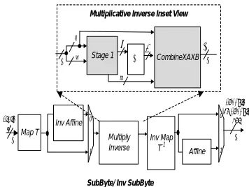
The proposed fault detection is presented using the new low-power and low-area S-box/ InvS-box architecture based on a compact composite field, using a polynomial basis. The transformation of the S-box uses an irreducible polynomial of p(x) = x8+x4+x3+x+1 to construct the binary field, GF(28). It consists of multiplicative inversion, followed by an affine transformation.
hardware complexity of the circuit consists of Stage 1, the inversion and the combination of multiplication in GF(24). Stage 1 includes a logic optimisation of multiplication in GF(24), multiplication with constant, squaring in GF(24), and addition included in one circuit. CombineXAXB is minimised for multiplication in GF(24) after multiplicative inversion in GF(24). The implementation of differential blocks and predicted parities are obtained by using the best choice of φ = {10}2 and λ={1000}2 to obtain the low area
and critical path delay. The new architecture as shown in Figure 1 reduces the gate count compared to a typical circuit using typical composite field architecture.
Stage 1 X-1 CombineXAXB
8 4 8
4
Map T Inv Affine
Multiply Inverse 0
1
Inv Map T-1
Affine 0
1
8
SubByte/ Inv SubByte Multiplicative Inverse Inset View
8 State
in
SubByte/ Inv SubByte
out
θ Λ
m q
4 4 g
4
[image:2.595.310.560.53.149.2]w
Figure 1: New S-box/ InvS-box architecture New proposed fault detection scheme architecture
The fault detection scheme has been developed by comparing the actual parity output, and predicted parity output results in the error indication flag for the corresponding block. The architecture of S-box and inverse S-box have been divided into seven blocks that cover each sub-structure inside it, with seven predicted parities. Seven error indication flags are observed, and for zero error computation, the output of flags should be zero when compared with the actual parities. The predicted parity is obtained using the input of each block, while the actual parity is obtained from the output of each block. XOR gate implementation is utilized to compare the two parity outputs and to obtain the fault indication flag. We optimized the logic area complexity for each of the predicted parity units, to cover all faults, in every output of the S-box/ InvS-box. Each block of the S-Box is modified in order to detect all single faults leading to an odd number of errors in the output.
Figure 2 illustrates the block diagram of the proposed parity prediction fault detection blocks, for the composite field S-box and InvS-box. Blocks 1 and 6 cover the fault detection for isomorphic and inverse isomorphic, while blocks 2 and 7 consist of affine and inverse affine predicted parity. Blocks 3, 4 and 5 were developed to implement the fault detection for multiplicative inversion transformation, consisting of Stage 1, inversion in GF(24), and multiplication in GF(24) (CombineXAXB).
Stage 1
Combine XAXB X-1
8 8
4 4 Isomorphic
InvAffine 0
1
Inv Isomorphic
Affine
0
1
8 8
Data out Data
in
ρiso ρinvaffine ρstage1 ρinversion ρCAB ρinviso ρaffine err1 err2 err3 err4 err5 err6 err7
Figure 2: Proposed parity prediction fault detection blocks for the composite field S-box and InvS-box
Sub-block of Fault Detection Scheme
A. Blocks 1 and 6: Predicted Parity of Isomorphic and
Inverse Isomorphic Mapping
Blocks 1 and 6 represent the isomorphic and inverse isomorphic mapping based on φ = {10}2 and λ=
{1000}2, for the best optimum logic implementation to
obtain the low area and critical path delay.
Lemma 1: Let
ς
= {ς
7
ς
6ς
5ς
4ς
3ς
2ς
1ς
0} be the input of isomorphic mapping in GF(24) andΓ
={
Γ
7Γ
6Γ
5Γ
4Γ
3Γ
2Γ
1Γ
0} be the input of predicted parities of isomorphic mapping. The derivation for the predicted parities of block 1, ρiso is as follows:𝜌𝜌𝑖𝑖𝑖𝑖𝑖𝑖=
ς
0+ς
1+ς
2+ς
5 (1)The total number of XOR gates needed for implementation of block 1, 𝜌𝜌𝑖𝑖𝑖𝑖𝑖𝑖 in the S-Box/ InvS-box is three XOR gates illustrated in Figure 3.
XOR
ς
0ς
1ρ
iso =ς
XOR XOR2
ς
5 [image:2.595.75.253.232.366.2]ρ
isoFigure 3: Predicted Parity of Isomorphic Mapping
Lemma 2: Let
Λ
= {Λ
7Λ
6Λ
5Λ
4Λ
3Λ
2Λ
1Λ
0} bethe input of inverse isomorphic mapping in GF(24), and
Γ
′= {Γ
′7Γ
′6Γ
′5Γ
′4Γ
′3Γ
′2Γ
′1Γ
′0} be the input of the predicted parity of inverse isomorphic mapping. The predicted parity of block 6, 𝜌𝜌𝑖𝑖𝑖𝑖𝑖𝑖𝑖𝑖𝑖𝑖𝑖𝑖 is obtained as follows:𝜌𝜌𝑖𝑖𝑖𝑖𝑖𝑖𝑖𝑖𝑖𝑖𝑖𝑖 =
Λ
0+Λ
2+Λ
6+Λ
7 (2)XOR
Λ
0Λ
2ρ
inviso = XOR XORΛ
6Λ
7ρ
inviso [image:2.595.332.515.465.534.2] [image:2.595.333.544.651.749.2]Figure 4 shows the hardware implementation complexity for the predicted parities of block 6, 𝜌𝜌𝑖𝑖𝑖𝑖𝑖𝑖𝑖𝑖𝑖𝑖𝑖𝑖 consists of three XOR gates.
B. Block 3: Parity Stage 1
Block 3 of the S-Box/InvS-box implements Stage 1 architecture, which consists of multiplication in GF(24), multiplication with lambda, squaring in GF(24) and a modulo-2 addition process based on composite field arithmetic.
The predicted parity of block 3, Pstage1 as follows:
Lemma 3: Let the input of Stage 1 be 𝑤𝑤= {𝑤𝑤3𝑤𝑤2𝑤𝑤1𝑤𝑤0}R2
and 𝑞𝑞= {𝑞𝑞3𝑞𝑞2𝑞𝑞1𝑞𝑞0}R2, while 𝛾𝛾= {𝛾𝛾3𝛾𝛾2𝛾𝛾1𝛾𝛾0}R2 is the
input of the predicted parity of Stage 1. The predicted parity of block 3, 𝜌𝜌𝑖𝑖𝑠𝑠𝑠𝑠𝑠𝑠𝑠𝑠1as follows:
𝜌𝜌𝑖𝑖𝑠𝑠𝑠𝑠𝑠𝑠𝑠𝑠1= (𝑤𝑤0∪(𝑞𝑞0+𝑞𝑞1+𝑞𝑞2+𝑞𝑞3)) +𝑤𝑤1(𝑞𝑞0+𝑞𝑞2)
+ 𝑤𝑤2(𝑞𝑞0+𝑞𝑞1+𝑞𝑞3) +𝑤𝑤3(𝑞𝑞0+𝑞𝑞2+𝑞𝑞���3) (3)
where ∪ represents the OR operation.
The hardware implementation of the predicted parity for block 3 requires seven XOR gates, three AND gates, one OR gate, and one inverter gate, as shown in Figure 5.
XOR
q
0ρ
stage1= XOR XORq
2q
3q
1OR
w
0AND
XOR AND XOR
XOR
XOR AND
w
1w
2w
3NOT
XOR
[image:3.595.46.291.382.548.2]ρ
stage1Figure 5: Predicted parity for Stage 1 implementation
C. Block 4: Parity Inversion
Lemma 4: Let the input of the inversion in GF(24) be
𝛾𝛾= {𝛾𝛾3𝛾𝛾2𝛾𝛾1𝛾𝛾0}R2 and 𝛳𝛳= {𝛳𝛳3𝛳𝛳2𝛳𝛳1𝛳𝛳0}R2 is the input for
the predicted parity of the inversion. The derivations of the predicted parity inversion, ρ𝑖𝑖𝑖𝑖𝑖𝑖𝑠𝑠𝑖𝑖𝑖𝑖𝑖𝑖𝑖𝑖𝑖𝑖 are obtained as follows:
ρ𝑖𝑖𝑖𝑖𝑖𝑖𝑠𝑠𝑖𝑖𝑖𝑖𝑖𝑖𝑖𝑖𝑖𝑖 =𝛾𝛾0(������𝛾𝛾2𝛾𝛾�1) +𝛾𝛾3(𝛾𝛾0+𝛾𝛾1) (4)
XNOR
y
2y
1ρ
inversion=
XOR
y0
NOT
AND
y
3AND XOR
ρ
inversionFigure 6: Predicted parity for inversion in GF(24) implementation
Figure 6 illustrates the hardware implementation for the predicted parity of inversion, which utilizes two XOR gates, two AND gates, one NAND gate and one inverter.
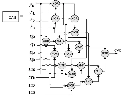
D. Block 5: Parity CombineXAXB
Block 5 consists of two multiplications in GF(24), after the multiplicative inverse of nibble in GF(24). The architecture is optimised using a Boolean simplification technique in order to achieve a low gate count.
Lemma 5: Let 𝛳𝛳= {𝛳𝛳3𝛳𝛳2𝛳𝛳1𝛳𝛳0}R2, 𝑚𝑚= {𝑚𝑚3𝑚𝑚2𝑚𝑚1𝑚𝑚0}R2
and 𝑞𝑞= {𝑞𝑞3𝑞𝑞2𝑞𝑞1𝑞𝑞0}R2 be the input of CombineXAXB,
while 𝛬𝛬= {𝛬𝛬7𝛬𝛬6𝛬𝛬5𝛬𝛬4𝛬𝛬3𝛬𝛬2𝛬𝛬1𝛬𝛬0}R2 is the input for the
predicted parity of CombineXAXB. The derivation of the the predicted parity is:
ρ𝐶𝐶𝐶𝐶𝐶𝐶= (𝛹𝛹+𝛳𝛳3)(𝑞𝑞3+𝑚𝑚3) + (£ +𝛳𝛳0)(𝑞𝑞2+𝑚𝑚2) +
𝛹𝛹(𝑞𝑞1+𝑚𝑚1) + €(𝑞𝑞0+𝑚𝑚0) (4) where𝛹𝛹=𝛳𝛳2+𝛳𝛳0, £ =𝛳𝛳1+𝛳𝛳3 and € =𝛹𝛹+ £
XOR θ0
ρCAB = θ XOR XOR
2
θ3
θ1
XOR
XOR
AND q0
q2
q1
q3
m0
m2
m1
m3
XOR AND
XOR AND
XOR
XOR
XOR AND
XOR XOR ρ
[image:3.595.326.524.466.624.2]CAB
Figure 7: Predicted parity of CombineXAXB implementation
The number of gates required for implementing the predicted parity of block 5, ρ𝐶𝐶𝐶𝐶𝐶𝐶 is 15 XOR gates and four AND gates, as shown in Figure 7.
E. Blocks 2 and 7: Parity Affine and Inverse Affine
ρ𝑠𝑠𝑎𝑎𝑎𝑎𝑖𝑖𝑖𝑖𝑠𝑠 =𝑐𝑐�������+𝑏𝑏+����������������𝑏𝑏+𝑒𝑒+
Γ
′6+𝑎𝑎����������������+𝑑𝑑+Γ
′1 +𝑑𝑑�������+𝑐𝑐+𝑏𝑏+𝑒𝑒+𝑑𝑑 (5) where𝑎𝑎=
Γ
′4+Γ
′5,𝑐𝑐=𝑎𝑎+Γ
′6,𝑏𝑏=Γ
′0+Γ
′7,𝑑𝑑=
Γ
′2+Γ
′3 and 𝑒𝑒=Γ
′1+Γ
′5XOR
Γ’0
Γ’1
Γ’2
Γ’3
Γ’4
Γ’5
Γ’6
Γ’7
XOR
XOR
XOR
XOR XOR XOR XNOR
XNOR
XOR
XNOR XOR
XOR
XNOR
XOR
XOR
ρaffine =
[image:4.595.48.277.71.276.2]ρaffine
Figure 8: Predicted parity circuit of affine implementation Hardware implementation for the predicted parity of block 2, 𝜌𝜌𝑠𝑠𝑎𝑎𝑎𝑎𝑖𝑖𝑖𝑖𝑠𝑠 requires 12 XOR gates and four XNOR gates, as shown in Figure 8.
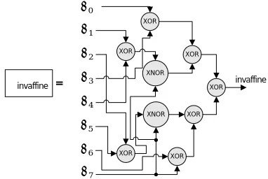
Lemma 7: Let the input of the inverse affine be
Γ
={
Γ
7Γ
6Γ
5Γ
4Γ
3Γ
2Γ
1Γ
0}. The predicted parity of Stage 1 is derived as follows:𝜌𝜌𝑖𝑖𝑖𝑖𝑖𝑖𝑠𝑠𝑎𝑎𝑎𝑎𝑖𝑖𝑖𝑖𝑠𝑠=𝛤𝛤���������������2+𝛤𝛤5+𝛤𝛤7+���������������𝛤𝛤1+𝛤𝛤4+𝛤𝛤7+𝛤𝛤0+𝛤𝛤3+𝛤𝛤6+
𝛤𝛤7 (6)
The number of gates needed for implementing the predicted parity of block 7, 𝜌𝜌𝑖𝑖𝑖𝑖𝑖𝑖𝑠𝑠𝑎𝑎𝑎𝑎𝑖𝑖𝑖𝑖𝑠𝑠 shown in Figure 9 is seven XOR gates and two XNOR gates.
ρinvaffine =
Γ0 Γ1 Γ2 Γ3 Γ4 Γ5 Γ6 Γ7
XNOR XOR
XOR XNOR XOR
XOR XOR
XOR XORρ
[image:4.595.305.560.139.267.2]invaffine
Figure 9: Predicted parity circuit of inverse affine implementation
DISCUSSIONS
The total area implementation for the fault detection predicted parity block of the S-box/ InvS-box required 49 XORs, six XNORs, nine ANDs, one inverter, two ORs and one NAND gate. Table 1 summarises the hardware complexities for each of the predicted parities for blocks 1- 7. Table 2 shows a comparison of the total hardware complexities between the proposed predicted parity and S-box/ Inv S-box with design of (Kermani and Masoleh, 2011). Design of (Kermani and Masoleh, 2011) only for S-box and their predicted parity architecture with the same φ = {10}2 andλ= {1000}2 as the proposed design.
[image:4.595.303.543.325.458.2]According to the table, the proposed fault detection scheme achieves the lowest core area through the circuit level optimization.
Table 1: Hardware complexities for proposed predicted parity of S-box/ InvS-box
Table 2: Comparison of total hardware complexities for different predicted parity of S-box/ InvS-box
Architecture Area of
S-box/ Inv
S-box
Area of parity prediction
Total area of S-box/ Inv S-box and parity prediction Mozaffari and
Arash, 2011 *only S-box
122X + 36A
42X + 9A + 3O + 1I
164X + 45A + 3O +1I Proposed 105X +
38A + 3N + 1O
49X + 9A + 2O +6XN +1I
154X + 47A + 3N + 3O + 6XN + 1I
X = XOR, A = AND, O = OR, I = NOT, N = NAND, XN = XNOR
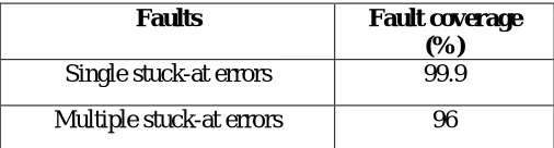
The proposed fault detection scheme was simulated using 130nm CMOS technology, in the Mentor Graphic environment. The evaluation for single stuck-at errors was carried out to evaluate the fault coverage of the proposed fault detection.
The actual parities for each block of the S-box/ InvS-box required an XOR gate to obtain the output parity, to compare with the predicted parity. Furthermore, seven XOR gates are needed to obtain the indication flag, by comparing seven of the predicted blocks with the actual parities. All possible single stuck-at errors were inserted randomly on the input and output nodes of the logic gates of the S-box. Fifty data inputs for the S-box/InvS-box were selected and the correct input of each block was replaced by an erroneous value, corresponding to a stuck-at fault at an input line of each block. The output error is detected by comparing the parity bit with the actual parity of the outputs. All the single faults will result in single errors in an odd number of erroneous bits at its output, and all the possible faults are detected by parity checking at each of the blocks and ends of the S-box/ InvS-box block.
The proposed fault detection was also injected with multiple stuck-at errors, whereby 50 nodes were made faulty for a multiple fault. This simulation proves that the predicted parity fault detection has almost 100% fault coverage at the byte level. For a single stuck-at error, it shows that the faults are covered 99.9 % for both entire Block XOR XNOR AND INV OR NAND
1, 𝝆𝝆𝒊𝒊𝒊𝒊𝒊𝒊 3 - - - - -
2, 𝝆𝝆𝑠𝑠𝒇𝒇𝒇𝒇𝒊𝒊𝒇𝒇𝒇𝒇 12 4 - - - - 3, 𝝆𝝆𝑺𝑺𝑺𝑺𝑺𝑺𝑺𝑺𝒇𝒇𝑺𝑺 7 - 3 1 1 4, 𝝆𝝆𝒊𝒊𝒇𝒇𝒊𝒊𝒇𝒇𝒊𝒊𝒊𝒊𝒊𝒊𝒊𝒊𝒇𝒇 2 - 2 - 1 1
5, 𝝆𝝆𝑪𝑪𝑪𝑪𝑪𝑪 15 - 4 - - -
6, 𝝆𝝆𝒊𝒊𝒇𝒇𝒊𝒊𝒊𝒊𝒊𝒊𝒊𝒊 3 - - - - - 7, 𝝆𝝆𝒊𝒊𝒇𝒇𝒊𝒊𝑺𝑺𝒇𝒇𝒇𝒇𝒊𝒊𝒇𝒇𝒇𝒇 7 2 - - - -
[image:4.595.68.259.490.618.2]SubBytes and inverse SubBytes. For multiple stuck-at errors, a 96% fault coverage resulted, which covers 48 nodes that were identified from the 50 injected nodes in both the S-box and the inverse S-box. Table 3 represents the fault coverage for single and multiple stuck-at errors for the S-box and inverse S-box.
Table 3:Fault coverage for fault detection scheme
Faults
Fault coverage
(%)
Single stuck-at errors
99.9
Multiple stuck-at errors
96
CONCLUSION
In this paper, the new fault detection scheme, based on parity bits, has been developed for the S-box/ Inv S-box architecture. It has been shown that the proposed fault detection scheme, using the new optimum composite field S-box/ InvS-box, has lower complexities and delay overheads than other previous designs. Based on the simulation results, high fault coverage was obtained for the proposed fault detection scheme. This scheme also offers low hardware complexities, which leads to a low cost and low power design estimated about 20uW.
ACKNOWLEDGEMENT
This research was conducted with financial support by Short Term Grant (STG) Vot Number 1328.
REFERENCE
Bertoni, G., Breveglieri, L., Koren, I., Maistri, P. and Piuri, V., (2003). Error analysis and detection procedures for a hardware implementation of the advanced encryption standard. IEEE Transactions on Computers, 52, pp. 492-505.
Bousselam, K., Di Natale, G., Flottes, M. and Rouzeyre, B., (2010). Evaluation of concurrent error detection techniques on the advanced encryption standard. 2010 IEEE 16th International On-Line Testing Symposium (IOLTS), pp. 223-228.
Di Natale, G., Flottes, M. L. and Rouzeyre, B., (2007). A Novel Parity Bit Scheme for SBox in AES Circuits. IEEE Design and Diagnostics of Electronic Circuits and Systems DDECS '07, pp. 1-5.
Jemima Anlet, M. J. P., (2012). Parity Based Fault Detection Approach for the Low Power S-Box and Inverse S-Box. International Journal of Computer Technology and Electronics Engineering. 2, pp. 76-81.
Karri, R., Wu, K., Mishra, P. and Yongkook, K., (2002). Concurrent error detection schemes for fault-based side-channel cryptanalysis of symmetric block ciphers. IEEE
Transactions on Computer-Aided Design of Integrated Circuits and Systems, 21, pp. 1509-1517.
Mozaffari, K. M. and Arash, R.-M., (2011). A Lightweight High-Performance Fault Detection Scheme for the Advanced Encryption Standard Using Composite Fields. IEEE Transactions on Very Large Scale Integration (VLSI) Systems, 19, pp. 85-91.
Mozaffari, K. M. and Arash, R.-M., (2007). A Structure-independent Approach for Fault Detection Hardware Implementations of the Advanced Encryption Standard. Workshop on Fault Diagnosis and Tolerance in Cryptography FDTC 2007, pp. 47-53.
Mozaffari, K. M. and Arash, R.-M., (2006). Parity-Based Fault Detection Architecture of S-box for Advanced Encryption Standard. 21st IEEE International Symposium onDefect and Fault Tolerance in VLSI Systems DFT '06 , pp. 572-580.
Satoh, A., Sugawara, T., Homma, N. and Aoki, T., (2008). High-Performance Concurrent Error Detection Scheme for AES Hardware. Cryptographic Hardware and Embedded Systems – CHES 2008. 5154, pp. 100-112.