The Design of High Performance Asynchronous
Pipelines with Quasi Delay Insensitive
D. Jayanthi
Associate Professor, Dept. of ECE Sona College of Technology, Salem.
M. Rajaram
Vice-Chancellor
Anna University of Technology, Tirunelveli
ABSTRACT
VLSI Design looking towards to solve design constructions that arises when using clock pulses. The majority of the constrains can be overcome by using asynchronous logic, additionally synchronous circuits has some inherent advantages over synchronous counterparts. This paper demonstrates the design of efficient asynchronous pipelines for some standard logic circuits and medium scale integration (MSI) circuits. The performance analysis of various templates is designed for different standard logics and MSI circuits. The QDI templates are highly tolerant of process variations due to the up and down transitions are sensed. QDI circuits are quite robust in terms of process variations and design tolerances. In this work, expose a timing assumption used in staticizers for QDI logic and apply it to other parts of circuits. Goal of this work is to optimize circuits with respect to area and power while maintaining the robustness.
Keywords
Asynchronous Channels, QDI Templates PCHB, PCFB and RSPCHB.
1.
INTRODUCTION
Asynchronous design which replaces [1] [2]clocking local handshaking has the potential to make high speed design more feasible Hence facilitating modular and reusable design .So that the localized control
of asynchronous pipeline is an excellent match for very high throughput fine grain data path. Asynchronous design which replaces [3] global clocking local handshaking has the potential to make high speed design more feasible. Asynchronous design has recently attracted industry [4] [5] due to its potential for low power consumption, low electromagnetic interfaces, high speed and robust interfacing. The focus of this paper is on a key enabling technology to make high speed asynchronous system practical, and the design of high throughput asynchronous pipelines. In the design of asynchronous systems, the global clock is eliminated and replaced [6] with local handshake channels which only communicate when and where necessary. Among the protocols used for handshaking, the micropipeline concept is first proposed in. An Asynchronous pipeline style introduced [7] for high speed application, the pipeline uses standard blocks of standard logic for processing data and single level sensitive SR latches to separate data items. This approach includes[8] a novel high-concurrent handshake protocol, with fewer synchronization points between neighboring pipeline stages than almost all existing asynchronous dynamic pipelining approaches. This study presents a
methodology for improving the speed of high-speed adders. As a starting point, a previously proposed method, called “speculative completion,” is used in which fast-terminating additions are automatically detected. Unlike the previous design, the method proposed in this study is able to adapt dynamically to (1) Application-Specific Behavior and (2) The latches worked on AMULET1 are level sensitive, so two- to four-phase converters are necessary in each latch controller. To avoid this transparency, an investigation has been carried out into four-phase micropipeline control circuits; this has terrified up several design issues telling to cost, performance and safety and forms a useful illustration of asynchronous design techniques. A robust asynchronous full adder design [9] corresponding to early output logic, synthesized using the elements of a standard cell library is presented in this study. As the name suggests, the adder ensures the gate orphan freedom and neatly fits into the self-timed system architecture. In comparison with many of the indicating full adder designs, which can be embedded in the self-timed system, it is found. These design estimates correspond to simulation results of the 32-bit carry-ripple adder circuit; derived by targeting a high speed 130 nm bulk CMOS process technology. Also, the proposed full adder facilitates a faster reset and the return-to-zero for the fundamental carry-propagate topology is achieved with only two full adder delays. A QDI system is constructed as a collection of concurrent hardware modules (called processes) [10] that communicate with each other through message-passing channels. These messages consist of atomic data items called tokens, which are usually multi-rail encoded each process can send and receive tokens to and from other processes through one-to-one communication by means of handshake protocols. Due to the lack of global clock and multi-rail encoded data communication, QDI circuits have the potential to achieve self-checking and halt the circuit in the presence of failures. An asynchronous width adaptive data architecture that [11] activates operations only in significant data portions and adjusts the position of sign bit dynamically. This architectural approach [12] yields good average-case performance and reduces power consumption, but the representative implementation is based on the quasi-delay-insensitive asynchronous design style, which is known to be area expensive.
2.
Asynchronous channels
Fig 1: Hand shakes protocol
Fig. 1.A protocol that can be sending by sender through channel, this is called push channel, the opposite the receiver asking for new data is called pull channel. In both cases the directions of the request and acknowledge signals are reversed and the validity of data is indicated in the
acknowledge signals from the sender to the receiver. The associated channel is called a bundled-data channel. Alternatively, if the data is sent using two wires for each bit of information, the encoding is called a dual rail channel. Extensions to 1-of-N encoding also exist. Both single-rail and dual-rail encoding schemes are commonly used and there are tradeoffs between each. Dual-rail and 1-of-N encodings allow for data validity to be indicated by the data itself and are often used in QDI designs. Single-rail, in contrast, requires the associated request line, driven by a matched delay line, to always be longer than the computation. This latter approach requires careful timing analysis but allows the reuse of synchronous single-rail logic.
3. MATERIALS AND METHODS
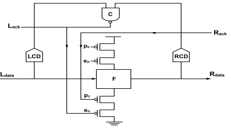
[image:2.595.80.233.79.270.2]PCHB: The Fig.2 below shows the template for Pre-Charged Half Buffer (PCHB).The test for validity and neutrality is confirmed using an input end detector Weak-conditioned half buffer(WCHB).This input end detector is denoted by LCD while its output end detector is denoted by RCD.
Fig 2:PCHB
In order for the functions block to evaluate before all the inputs have arrived, it need not be weak conditioned. On the other hand, the template only generates an acknowledgement signal Lack after all the inputs have arrived and output has been evaluated. The LCD and RCD are therefore combining using a C-element to generate the acknowledgement signal. Pointing out some aspects of this template; first, as the C-element is inverting
the acknowledgement Signal is an active low signal. Second the Lack signal is after buffering using the inverters before being sent out usually, two other inverters are added to buffer the internal signal en that controls the
function block.A WCHB is handy for buffers, but the precharge half buffer (PCHB) is
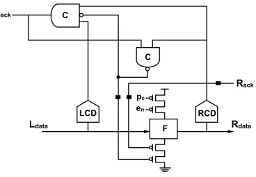
[image:2.595.82.477.372.592.2]Fig 3: PCFB
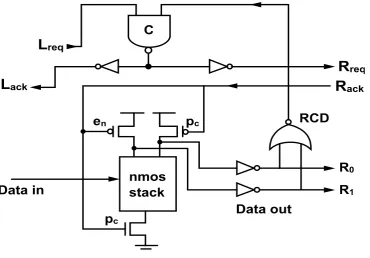
Proposing a new pipeline template eliminating the need of the internal en signal of the PCHB template reducing the transition stack sizes in the function block. This new QDI pipeline template is referred to as a Reduced Stack Pre-Charged Half Buffer (RSPCHB) as shown in Fig.4.It is noted that the RCD block is optimized by tapping its inputs before the output inverter and a NAND gate is used instead of an OR gate. RSPCHB template facilitates the removal of the internal enable signal by reducing concurrency that does not improve performance. In the PCHB templates the output of LCD and RCD are companied using a C-element to generate acknowledgment signal Lack. As a result integration of the handshake protocol with the validity and neutrality of both input and output data is supported .This gets rid of the need for function block to be weak conditioned .Though requires
[image:3.595.86.455.99.354.2]Fig 4: RSPCHB
This delay prevents the precharge from triggering the RCD to deassert. Further preventing the C-element from ever generating the acknowledgment. The en signal could be safely removed if generation of acknowledgment signals from any stage subsequent to the join has arrived and been acknowledged .The join been the performance bottleneck for the subsequent stages, delay of the acknowledgment would not impact performance. The advantage of RSPCHB is that the lack of an LCD and reduced stack size of the function block, which reduces capacitive load and
yields significantly faster overall performance. The cost of this increase in performance is that it requires one extra communicating wire between stages.
4.Result
[image:4.595.79.450.70.328.2]The latency of the five standard circuits for the PCFB, PCHB and RSPCHB templates are shown in Figure 5.
Fig 5.Forward latency of standard circuits across PCFB, PCHB, and RSPCHB templates
0 20 40 60 80 100 120 140
and_2 or_2 xor_2 FA_3 Mux_4_1
Fo
rwar
d
Late
n
cy
(
ρ
s)
PCHB
PCFB
On average, the latency of the PCHB is 6.5% less than the other circuit templates. The PCHB generally offer lower latency based onRe and Le are combined in a separate c-element, rather than in the data rail stacks. The RSPCHB
has a similar latency to the PCFB except and_2 and or_2 circuits where it’s 6.5% slower.
Fig 6.Total transistor area of standard circuits across PCFB, PCHB and RSPCHB templates
.
The pull down stacks in these circuits was augmented to wait for input validity, which makes them slower. Figure 6 shows a comparison of the total transistor area across the standard circuits. An interesting result is that the PCHB is slightly smaller than the PCFB. Once again, this is
attributed to its simpler data rail transistor stacks. The RSPCHB is about 15.7% smaller than the PCHB template and 20.3% smaller than the PCFB template on average. This is a result of the simplified detection of input neutrality possible with the half cycle timing assumption.
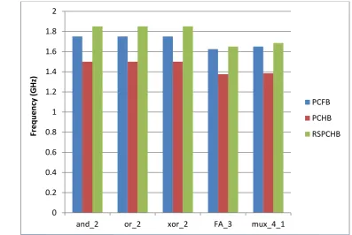
Fig 7. Frequency of standard circuits across PCFB, PCHB, and RSPCHB templates.
0 1 2 3 4 5 6 7 8
and_2 or_2 xor_2 FA_3 Mux_4_1
To
tal Tr
an
si
sto
r Ar
e
a(µ
m
2)
PCFB
PCHB
RSPCHB
0 0.2 0.4 0.6 0.8 1 1.2 1.4 1.6 1.8 2
and_2 or_2 xor_2 FA_3 mux_4_1
Fr
e
q
u
e
n
cy
(GHz)
PCFB
PCHB
[image:5.595.100.498.447.713.2]The HCFB template is consistently higher frequency than the other templates across all five standard circuits, as seen in Figure 7. On average, the HCFB is 7.5% higher frequency than the PCFB. The PCHB has an 18 transition cycle time and the RSPCHB and PCFB both have a 14 transition cycle time. However, the RSPCHB offer higher frequency based on many of its transitions, especially those that detect input neutrality, are simpler. This suggests that HCFB can use even less area and smaller transistors for these fast transitions to match the frequency
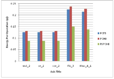
of the PCFB.The energy per operation (or per cycle) of the standard circuits is reported in Figure 8. The RSPCHB template consistently uses less energy than the PCFB and PCHB templates across all five standards. The RSPCHB template consumes 30% and 34% less energy on average than the PCFB and PCHB templates respectively. This is comparatively good based on its significant area savings, a slight frequency improvement, and a negligible latency penalty.
5.
PERFORMANCE
OF
EVALUVATION
Simulations are done with HSpice e using model files with 64.5 nm process. Each output node added by 4fFwire capacitance. This amount of capacitance is typical of short
wires based on extracted layout in this technology. Gates are sized to have the drive strength of an inverter with its pmos width set to 20 lambda units and its nmos width set to 10 lambda units(lambda is defined as half the minimum gate length). All power and energy numbers are based on
total dissipated power.
[image:6.595.122.497.319.578.2].
Fig. 8: Energy per operation of standard circuits across PCFB, PCHB, and RSCHB templates.
6. CONCLUSION
We investigated basic primitives with MSI circuits based
on various asynchronous QDI
predesigned templates. Using these styles, logic gates and some MSI circuits have been designed and simulated by Tanner EDA tool.
The author believe that the proposed design will provide a platform for designing high speed, low power digital circuits such as pipelined multiplier implemented in any application of digital signal processors.
7. REFERENCES
[1].Montek singh and steven M.Nowick The design of High performance dynamic asynchoronous pipelines; Lookahead style IEEE Transactions on Very Large Scale Integration systems.2007.
[2] Alain J. Martin ,Asynchronous Techniques for System-on-Chip Design, Vol. 0018- 9219_2006.IEEE 94, No. 6, June 2006 , Proceedings of the IEEE.
Univ., Stanford, CA, 1984, Stanford CS Tech. Rep. STAN-CS-84-1026.
[4].LARS S. NIELSEN AND JENS SPARSO, Designing Asynchronous Circuits for Low Power:An IFIR Filter Bank for a Digital Hearing Aid, proceedings of the ieee, vol. 87, no. 2, February 1999.
[5].J. Cortadella et al., Logic Synthesis of Asynchronous Controllers and Interfaces. New York:Springer-Verlag, 2002.
[6]I.E.Sutherland,“Micropipelines," Commun. ACM, vol. 32, pp. 720-738,Jun 1989.
[7] Montek Singh and Steven M. Nowick, “MOUSETRAP: High-Speed Transition- Signaling Asynchronous Pipelines”, IEEE transactions very on large scale integration (VLSI) systems, vol. 15, no. 6, June 2007.
[8]. Furber, S.B. and P. Day, 1996. Four-Phase Micropipeline Latch Control Circuits. IEEE Trans.
Very Large Scale Integration (VLSI) Syst., 4: 247- 253. DOI: 10.1109/92.502196.
[9].Balasubramania, P., 2011. A Robust Asynchronous Early Output Full Adder. WSEAS, Trans. Circuits Syst., 10: 221-230.
[10]. LaFrieda, C. and R. Manohar, 2009. Reducing power consumption with relaxed quasi delay-insensitive circuits. Proceedings of the 15th IEEE Symposium on Asynchronous Circuits and Systems, May 17- 20, IEEE Xplore Press, Washington, USA, pp: 217-226. DOI: 10.1109/ASYNC.2009.9.
[11].AlainJ.Martin ,Asynchronous Techniques for System-on-Chip Design, Vol. 0018- 9219_2006.IEEE 94, No. 6, June 2006 , Proceedings of the IEEE.