Speed & Area Efficient ASIC Design of FIR filter
for Satellite Applications
Vivek Kumar 1, Rajesh Mehra2, Shallu 3
1, 2, 3
ECE Department, NITTTR, Chandigarh, India
Abstract: In this paper, an Application Specific Integrated Circuit (ASIC) for FIR band-pass filter used in Satellite communication is implemented. Basically, two filter structures, Direct Form and Direct Form Symmetric are taken into consideration. ASIC implementation is carried out using 90nm complementary metal-oxide semiconductor (CMOS) Technology. Here, the main focus of the work is to select filter structure utilizing less area and providing higher speed. This band-pass FIR filter is used in between modulator and up-convertor of C band uplink model for satellite. The hardware result shows that the proposed FIR band pass filter with Direct–Form Symmetric FIR structure uses 0.5% less chip area & 3% less time delay as compared to filter with Direct-Form structure.
Keywords: Application Specific Integrated Circuit (ASIC), FIR, Band- pass filter, Direct Form Symmetric, Kaiser Window.
I. INTRODUCTION
Due to enhancement in digital signal processing (DSP) based applications like latest communication systems, mobile communication, and multimedia which demands efficient hardware and very low power operations. Digital filters are widely used for band selection, signal analysis, signal estimation, signal preconditioning.[1]. They are of two types, one is Finite Impulse Response Filter (FIR filter) and another is Infinite Impulse Response Filter (IIR filter)[2].FIR filter exhibits linear phase behaviour and bounded-input-bounded-output stability[3]. A band-pass filter allows a range of frequencies to pass through it [4]. FIR filters can be extensively used in communication systems to perform various functions like pulse shaping, channelization, matched filtering etc [5]. The reconfigurable filters based on digital signal processor cores or field programmable gate arrays provide advantage of flexibility and high sampling rates but they are not suitable for mobile devices which require small area, low power consumption and high throughputs. Since in such applications the reconfigurability of multiplier is not necessary therefore application specific integrated circuit (ASIC) can be used to satisfy the constraints of area, performance and energy utilization [6]. Integrated circuits are main components in digital signal processing, embedded systems, communication systems and electronic devices etc. [7]. The integrated circuits are constructed by using complementary metal-oxide semiconductor (CMOS) Technology. This technology is also known as complementary –symmetry metal-oxide semiconductor as it uses complementary and symmetrical pairs of both p and n type semiconductor field effect transistor. The CMOS technology allows large number of logic functions on a chip, which makes this technology suitable for implementing VLSI chip. The high noise immunity and low static power consumption are two main characteristics of CMOS devices [8]. There are two components of power consumption: dynamic power and leakage or static power. When the circuit performs function and signal changes, the dynamic power is consumed. Leakage power is consumed all the times, even when the circuit is idle[9].The cost of the circuit fabrication is directly proportional to the circuit area, so one of the main aim of the designer is to minimize the circuit area to reduce the chip cost[10]. For selection of best suited structure for proposed filter ASIC is designed and simulated for Direct-form FIR and Direct–Form Symmetric FIR structures. In this work, ASIC for both the structures are compared for area, time delay and power dissipation. On the basis of this comparison best suited structure is selected. The rest of the paper is organized as follows: satellite uplink model is presented in section II, the MATLAB based filter design using Kaiser Window and its various responses are illustrated in section III, section IV describes the RTL Design & performance evaluation. Finally the conclusion is presented in section V.
II. SATELLITEUPLINKMODEL
encoder, modulator, band-pass filter, up-convertor, high power amplifier and antenna as shown in fig.1 [11]. The input baseband signal is applied to encoder system and passes through modulator trail. The output of modulator is the input for band-pass filter. This is the proposed band-pass filter. The output of this stage is entered in up-convertor. After up conversion the signal is amplified by high power amplifier and the antenna transmits the signal in space towards satellite.
Fig.1 Block diagram of a satellite uplink model [11]
III.MATLABBASEDFILTERDESIGN
In digital signal processing the finite impulse response (FIR) filter is a kind of filter whose impulse response is of finite length [12]. The main components of FIR filter are large number of adders, delay elements and multipliers [13]. An FIR filter is described by following difference equation [14]:
(1)
Where y(n) is the current output sample of the filter, h(k), k= 0, 1, 2………L-1, are the impulse response coefficients of the FIR filter, x(n-k) is the input sample sequence of k-th times. L = Filter length, L-1= filter order. The filter length indicates the number of filter coefficients. The output sample y(n) is a weighted sum of the present input x(n) and L-1previous samples of the inputs. The transfer function of FIR filter is given by[15]
(2)
The Direct-Form FIR structure of FIR Filter: Sometime also known with the name transversal or tapped delay structure. The direct- form realization follows the non-recursive difference equation given by (1). The structure is given in fig.2 [16]. In the figure given below the symbol z-1 represents a delay of one sample. This structure requires L-1 memory location for storing L-1 previous inputs. structure has complexity of L multiplications and L-1 additions per output point.
Fig.2 Direct-Form FIR structure [16]
The Direct-Form FIR Symmetric structure of FIR Filter: It is also called linear phase structure. The structure is given in fig.3 [15] If the unit sample response of an FIR filter satisfies the following condition then the filter has linear phase:
This structure takes the advantage of symmetry to reduce the computational complexity of filter implementation. Here there is reduction in both the number of multiplications as well as additions. By taking account of this symmetry the filter equation can be re-written as follows:
When L is Odd
(4) When L is even
(5)
Fig.3 Direct-Form FIR Symmetric structure [16]
The frequency response hd(n) of an ideal filter is an infinite and non causal sequence but in practical filter it must be finite. In
practical applications, to make the sequence finite, the finite length window function {w (n)} is used. The frequency response, h(n) of an practical filter is given by[17]
(6)
The various techniques for FIR filter designing are windowing algorithm, least square, equiripple algorithm and so on[18]. Out of these Windows technique is used here. The popular window functions are Rectangular, Hanning, Hamming, Blackman and Kaiser Windows etc [19]. The window functions described above except Kaiser Window have fixed characteristics such as transition width (ΔF) and stop band attenuation (A)[20]. The Kaiser window provides variable transition width by using a ripple control parameter (β). Hence, the Kaiser window is used for designing. The Kaiser Window function is expressed as [21]:
(7) Where I0 (x)
is zero-order modified Bessel function of the first kind.
The value of β can be obtained from the following empirical relations [19]
(5)
Where A ( stop band attenuation)= - 20 log10 (α)
α = min(αs , αp ) , where αs= stop band ripple and αp = pass band ripple. The filter length or number of filter coefficient is given by [19]
Where ΔF = normalized transition width.
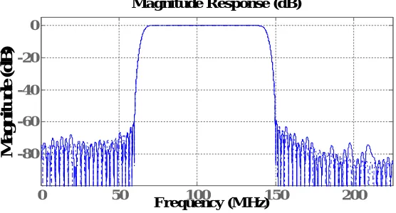
[image:5.612.185.429.166.310.2]The FIR band pass filter is designed in MATLAB environment with filter specifications having pass band frequency 70MHz to 140 MHz, sampling frequency 450MHz, pass band ripple is 1dB, transition frequency 10MHz, stop band attenuation is 60dB. Thus the filter has two stop bands 0-60MHz, the lower stop band and another stop band is 150-210 MHz, the upper stop band. The order of the filter is 164.
TABLE I. FILTER SPECIFICATIONS [11]
Parameter Name Value
Pass Band Frequency 70Mz-140 MHz
Pass Band Ripple 1dB Stop Band Attenuation 60 db Transition Width 10 MHz Lower Stop band
Frequency
0-60 MHz
Upper Stop band Frequency
150MHz-210MHz
Sampling Frequency 450 MHz
Magnitude Response: The graph plotted between magnitude in dB and frequency in MHz of the desired filter shows that it is flat within pass band i.e. from 70MHz to 140 MHz. In the stop band it provides 60dB attenuation.
0 50 100 150 200
-80 -60 -40 -20 0 Frequency (MHz)
M
a
g
n
it
u
d
e
(d
B
)
[image:5.612.156.434.372.522.2]Magnitude Response (dB)
Fig.4. Magnitude Response of band-pass filter
Phase response: The graph plotted between phase in radian and frequency in MHz shows that it is linear within pass band. Thus the desired filter has linear phase response.
0 50 100 150 200
-100 -80 -60 -40 -20 0 Frequency (MHz) P h a se ( ra d ia n s) Phase Response
[image:5.612.167.415.583.719.2]IV.RTLDESIGN
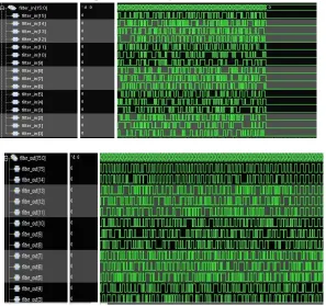
The Verilog hardware description language is used for design coding. The hardware realization of the proposed band –pass FIR filter in ASIC is achieved by using 90nm standard-cell technology by CAD Tools. Standard cell-based technology is widely used as a quick and efficient method to overcome the integrated circuit design complexity. In standard cell design style, the height of the cells is fixed to an integer multiple of a unit row height, but cell width can be variable [13]. The Adder Module and zoomed image of a portion of this module of Direct Form (DF) Symmetric structure is given in figure 6 and 7 respectively. The Multiplier Module and zoomed image of a portion of this module of Direct Form Symmetric structure is given in figure 8 and 9 respectively. The layout of FIR BPF filter with Direct Form (DF) Symmetric structure and zoomed image from a portion this layout is given in fig 10 and 11 respectively. The simulated Input /output waveform of FIR band pass filter with Symmetric structure is shown in fig.12
Fig.6 Adder Module of FIR BPF with DF Symmetric structure Fig.7 Zoomed image from a portion of Adder Module
Fig.8 Multiplier Module of FIR BPF with DF Symmetric structure Fig.9 Zoomed image from a portion of Multiplier Module
Layout of FIR band-pass filter with Direct Form Symmetric structure and Zoomed image from a portion of Layout of FIR BPF with Direct Form Symmetric structure is shown below:
The simulated Input /output waveform of FIR band pass filter with Symmetric structure is shown below:
Fig.12 Input and output waveform of FIR BPF with Direct Form Symmetric structure
Table II shows the comparison between band pass filter designed on ASIC with Direct-Form FIR structure and Direct-Form Symmetric FIR structure for area, delay time and power dissipation.
TABLE II. COMPARISON BETWEEN: DIRECT- FORM & DIRECT-FORM SYMMETRIC FOR RESOURCE UTILISATION
Parameter Direct- Form Direct-Form Symmetric
Area 169227.239 µm2 168344.114 µm2
Delay Time 13330ps 12887ps
Total Power Dissipation
1766020.140nW 2916924.584nW
The table II shows that the ASIC implementation of Band-pass FIR filter with Direct-Form FIR Symmetric structure used less chip area as well as faster in speed as compared to Band-pass FIR with Direct-Form structure. The power consumption is greater in Direct-Form FIR symmetric because there is always a trade-off between constraints like power and speed.
V. CONCLUSIONS
In this paper ASIC of band pass FIR filter for satellite communication with two structures Direct-Form FIR and Direct-Form Symmetric FIR is implemented. Comparison of results for resource utilization show that filter synthesized with Direct-Form Symmetric FIR structure uses 0.5% less chip area and 3% less delay time as compared to ASIC with Direct Form structure. Hence Direct-Form Symmetric FIR structure is speed and area efficient as compared to Direct-Form structure due to less number of multipliers and adders.
REFERENCES
[1] Nithish Kumar V, Koteswara Rao Nalluri and Lakshminarayanan G, “Design of Area and Power Efficient Digital FIR Filter Using Modified MAC Unit,” 2nd
International Conference on Electronics and Communication System (ICECS 2015), 2015, pp.884-887.
[image:7.612.162.459.88.367.2][3] Deepa Yagainl and Dr. Vijaya Krishna A, “FIR Filter Design Based on Retiming & Automation Using VLSI Design Metrics,” International Conference on Technology, Informatics, Management, Engineering & Environment (TIME-E 2013), 2013, Bandung, Indonesia, pp. 17-22.
[4] Ashu Soni, Sumit Kumar and Shivani Gupta “OTA model used in active and passive filter for lowering power consumption,” International Journal of Engineering Science & Research Technology (IJESRT) , vol. 2, No. 11, pp.3244-3247, Nov. 2013.
[5] Subhankar Bhattacharjee, Sanjib Sil and Amlan Chakrabarti, “Evaluation of Power Efficient FIR Filter for FPGA Based DSP Applications”, International Conference on Computational Intelligence: Modelling Techniques and Applications (CIMTA), 2013, pp.856-865.
[6] A.P. Vinod, A. Singla and C.H. Chang, “Low-power differential coefficients-based FIR filters using hardware-optimised multipliers,” IET Circuits Devices Syst., vol.1, Feb. 2007, No.1, pp. 13–22.
[7] Andreas Puhm and Peter Rössler, “Considerations on Teaching Digital ASIC Design,” 10th International Conference on Mechatronic and Embedded Systems
and Applications (MESA), 2014, pp. 1-6.
[8] Pooja Singh and Rajesh Mehra, “ Design Analysis of XOR Gates Using CMOS & Pass Transistor Logic,” National Student Conference On Advances in Electrical & Information Communication Technology(AEICT-2014), 2014, pp.-264 -267.
[9] Pushpa Saini and Rajesh Mehra, “ Leakage power reduction in CMOS VLSI circuits,” International Journal of Computer Applications , Volume 55– No.8,
pp.42-48, Oct. 2012
[10] Neil H. E. Weste and David Money Harris, CMOS VLSI Design_ A Circuits and Systems Perspective,4th ed., 2011.
[11] Aye Than, Zaw Min Naing, Chaw Myat New and Hla Myo Tun, “Development of digital band pass filter and antenna design for C band small satellite uplink model,” in IJSTR,vol.3, Issue7, pp.216-222, 2014.
[12] Kanu Priya and Rajesh Mehra, “Area efficient design of FIR filter using symetric strucure,” International Journal of Advance Reasearch in copmuter and communication Engineering, vol.1, issue 10, pp. 842- 845, 2012.
[13] Abdullah A. AlJuffri, Mohammed M. AlNahdi, AnasA. Hemaid, Osamh A. AlShaalan, Mohammed S. BenSaleh, Abdulfattah M. Obeid and Syed Manzoor
Qasim, “ASIC Realization and Performance Evaluation of Scalable Micro programmed FIR Filters using Wallace Tree and Vedic Multipliers,” IEEE 15th International conference on Environment and Electrical Engineering , 2015, pp.1995-1998.
[14] Vagner S. Rosa, Eduardo Costa, Jose C. Monteiro and Sergio Bampi, “Performance Evaluation of Parallel FIR Filter Optimizations in ASICs and FPGA,” 48th Midwest Symposium on Circuits and Systems, 2005, vol.2, pp. 1481-1484.
[15] Jayshri J. Patel, Dr. Kiran R. Parmar and Hardik N. Mewada, “Design of FIR Filter for Burst mode Demodulator of Satellite Receiver,” International Conference on Communication and Signal Processing, 2016, pp. 0686- 0690.
[16] John G. Proakis and Dimitris G. Manolakis, Digital Signal Processing Principles, Algorithms, and Applications, 3rd ed., 2002.
[17] Tushar Kanti Roy and Monir Morshed, “ Performance Analysis of Low Pass FIR Filters Design Using Kaiser, Gaussian and Tukey Window Function Methods,” 2nd International conference on Advances in Electrical Engineering, Dec. 2013, pp.1-6.
[18] Guo-Ming Sung and Hsiang-Yuan Hsieh “An ASIC design for decimation filter with canonic signed-digit representation,” International Symposium on Intelligent Signal Processing and Communication Systems (ISPACS2008), 2009, Swissôtel Le Concorde, Bangkok, Thailand,pp.1-4.
[19] GAO Jinding, HOU Yubao and SU Long, “Design and FPGA Implementation of Linear FIR Low-pass Filter Based on Kaiser Window Function,” Fourth
International Conference on Intelligent Computation Technology and Automation, 2011 pp. 496-498.
[20] Vivek Kumar, Rajesh Mehra and Shallu, “Reconfigurable band pass filter using Kaiser window for satellite communication,” 2nd International Conference on
Next Generation Computing Technologies (NGCT), 2016, pp.409-413.