Manufacturing of 64-Bit Vliw Microprocessor
Ajitender Kaur*
1, Ritesh Gaur
#2*M.Tech Scholar, Department of ECE, Kurukshetra University,Haryana, India #M.Tech Scholar, Department of ECE, Kurukshetra University,Haryana, India
Abstract-In the two decades since FPGAs introduced, the way which digital logic is designed and deployed has been radically changed. FPGAs have made possible entirely new types of applications. It is very important to design microprocessor as the part of core of electronic systems, so development and production. On making use of the technology of FPGA to design the microprocessor of logic function, it can quickly realize the function, complete design, cut down development cycle, save cost and quickly realize productions. The subject of the Paper is to design VLIW (is the abbreviation of "Very Long Instruction Word") microprocessor based on FPGA. It designs VLIW microprocessor which contains 64-bit instruction word and 192-bit data, each VLIW instruction word consists of three operations in parallel. The VLIW microprocessor can be designed using a pipeline technology of four stages, and have been implemented by taking advantage of the technology of FPGAs. According to the basic principle of VLIW microprocessor, it is rationally divided into five main modules: Fetch module, Decode module, Register file, Execute module, Write back module. Each main module is reasonably divided again, and realized the function of every module based on the principle of FPGAs, so as to implement five main modules.
INTRODUCTION
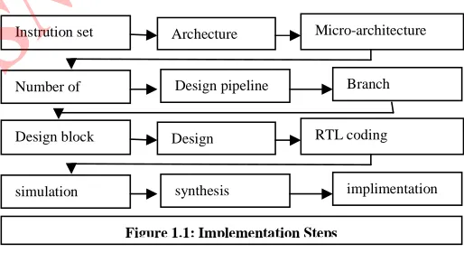
The objective is to design a 64-bit VLIW Microprocessor
supporting the following instruction set: addition, subtraction
and multiplication. Second objective is to model the dynamic
branch prediction in 4-stage 64-bit microprocessor to achieve
better throughput. Figure 1.1 shows the complete
implementation steps in designing a processor. The
programming objective of the pipelining fall into the
following categories:
1. Accuracy: The application produces that results that are close to the correct results.
2. Performance: The application produces the most efficient code possible.
3. Latency: The application produces a single output with in less time.
4. Throughput: The application produces more number of tasks that can be completed per unit time.
5. Area: The application produces less number of flip flops and slices.
TOOLS USED The tools used in the thesis are as follows: Simulation Software:
1. Xilinx 13.1 and design compiler are used for synthesis and analysis.
2. Modelsim 10.1 has been used for modeling and simulation. Hardware used:
Xilinx Spartan 3E (Family), XC4VFX12 (Device), Tool used
HDL (Top Level Source Type), XST-VHDL/VERILOG
(Synthesis Tool). ISE Simulator -VHDL/VERILOG
(simulator) and Verilog (Preferred Language).
Table : Comparison between CISC, RISC, VLIW Architecture [11]
Design block Design RTL coding
simulation synthesis implimentation Instrution set Archecture Micro-architecture
specification
[image:2.612.304.561.377.517.2]Number of Design pipeline Branch
VLIW (Very Long Instruction Word)
VLIW has been developed to exploit Instruction-Level
Parallelism by using a long instruction word which
contains multiple fixed numbers of operations. Those
operations can be fetched, decoded, issued, and executed at
the same time without causing any data or control hazards.
Therefore, all operations within a single VLIW instruction
must be absolutely independent. Very long instruction
word (VLIW) describes a computer processing architecture
in which a language compiler or pre-processor breaks
program instruction down into basic operations that can be
performed by the processor in parallel (that is, at the same
time). These operations are put into a very long instruction
word which the processor can then take apart without
further analysis, handing each operation to an appropriate
functional unit. VLIW is sometimes viewed as the next
step beyond the reduced instruction set computing ( RISC )
architecture, which also works with a limited set of
relatively basic instructions and can usually execute more
than one instruction at a time (a characteristic referred to as
superscalar). The main advantage of VLIW processors is
that complexity is moved from the hardware to the
software, which means that the hardware can be smaller,
cheaper, and require less power to operate. The Crusoe
family of processors from Transmeta uses very long
instruction words that are assembled by a pre-processor
that is located in a flash memory chip. Because the
processor does not need to have the ability to discover and
schedule parallel operations, the processor contains only
about a fourth of the transistor s of a regular processor. The
lower power requirement enables computers based on
Crusoe technology to be operated by battery almost all day
without a recharge. The Crusoe processors emulate Intel's
x86 processor instruction set. Theoretically, pre-processors
could be designed to emulate other processor architectures.
Crusoe- Crusoe is a family of "smart" microprocessors
from Transmeta that combines a relatively simple,
low-powered hardware processor with software that makes the
hardware processor look like an x86 Intel.
CONCEPT AND BENEFITS (VLIW)
In VLIW architecture, parallel execution of multiple
instructions is made possible by issuing a long instruction
word. A single long instruction word is designed to achieve
simultaneous execution of a fixed number of multiple
operations. Those operations must be independent of each
other to avoid possible data hazards. Indeed, several Architectu
res Characteri stis
CISC RISC VLIW
Instruction Size
Varies One size,
usually 32Bits One size Instruction Format Field placement varies Regular, consistent placement of fields Regular,cons istent placementof fields Instruction Semantics Variesfromim ple tocomplex; possiblymany dependent operations per
Almost always one simple operations Many simple, independent Operations Registers instruction Few, sometimes special Many, general-purpose Many, general-purpose Memory Reference s Bundled with operations in many
different types of Instructions
Not bundled with
operations, i.e., load/store architecture
Not bundled with operations, i.e., load/store architecture Hardware Design Focus Exploit microcode Implementati ons Exploit implementatio ns One pipeline &no microcode
No complex design
independent instructions are integrated inside a very long
instruction word.
The VLIW instruction is wide enough to allow the concurrent
operation of multiple functional units. Its size normally ranges
from 64 to 128 bits, and even up to 1024 bits. Figure above
shows a typical format of VLIW instructions. Many bits on
the long instruction enable a single instruction word to
sufficiently control the several functional units directly and
independently in every cycle. Since it is the long instruction
word which delivers the potential ILP to the hardware, a
VLIW processor can be designed with a simpler hardware
compared to an equivalent superscalar processor: it need not
include the special units the run-time dependency check and
instruction scheduling. The block diagram of a simple VLIW
processor is shown in Figure below. VLIW architecture is, by
essence, meant to activate multiple functional units at the
same time. Therefore, the VLIW compiler should uncover
independent operations to be executed in parallel. This means
that the compiler must perform a detailed analysis on the
data-flow and control-data-flow at compile time (which is when the
potential ILP is fixed). Since the ILP within a basic block is
quite limited, the VLIW architecture needs to examine more
instructions to find more ILP. It is possibly achieved by
looking at the instruction stream beyond the control-flow
limits. For that purpose, several techniques such as loop
unrolling and trace scheduling have been introduced in the
VLIW design techniques. In addition, VLIW can uncover
more parallelism by searching over a wider range of static
code. Also, it is quite beneficial to know the source code
structure to find parallelism in the VLIW architecture.
However, several limitations such as long compilation time,
not enough compatibility, and code explosion make VLIW
architectures difficult to use in practice [15]. In conclusion, we
can say that VLIW architectures do not have the hardware
complexity of current superscalar architectures. The two
approaches in the current high-performance microprocessor
design.
In the following Part, more detailed techniques for the
VLIW architecture is explained. The key to higher
performance in microprocessors for a broad range of
Memo
ry
operation
ALU operation
ALU operation
Branch operation
Figure: An Example of VLIW Instructions [16]
FU
FU
FU
FU
Register File
I-Cache External Memory
unit)
Decoding Unit
Fetch Unit
applications is the ability to exploit fine-grain,
instruction-level parallelism. [16]. some methods for exploiting
fine-grain parallelism include:
pipelining
multiple processors
superscalar implementation
specifying multiple independent operations per instruction
Pipelining is now universally implemented in
high-performance processors. Little more can be gained by
improving the implementation of a single pipeline. Using
multiple processors improves performance for only a
restricted set of applications. Superscalar implementations can
improve performance for all types of applications. Superscalar
(super: beyond; scalar: one dimensional) means the ability to
fetch, issue to execution units, and complete more than one
instruction at a time. Superscalar implementations are
required when architectural compatibility must be preserved,
and they will be used for entrenched architectures with legacy
software, such as the x86 architecture that dominates the
desktop computer market. Specifying multiple operations per
instruction creates a very-long instruction word architecture or
VLIW. A VLIW implementation has capabilities very similar
to those of a superscalar processor-issuing and completing
more than one operation at a time-with one important
exception: the VLIW hardware is not responsible for
discovering opportunities to execute multiple operations
concurrently. For the VLIW implementation, the long
instruction word already encodes the concurrent operations.
[17].This explicit encoding leads to dramatically reduced
hardware complexity compared to a high-degree superscalar
implementation of a RISC or CISC. The big advantage of
VLIW, then, is that a highly concurrent (parallel)
implementation is much simpler and cheaper to build than
equivalently concurrent RISC or CISC chips. VLIW is a
simpler way to build a superscalar microprocessor.
PIPELINING AND BRANCH PREDICTION MECHANISM
It is a technique that allows for simultaneous execution of
parts, or stages, of instructions to more efficiently process
them. It is first introduced in IBM 7030 (Stretch Computer).
1986 was the first pipelined CISC processor. RISC processors
in 80s were pipelined and were efforts to get IPC of 1. With a
RISC processor, 1 instruction is executed while the next is
being decoded and its operands are being loaded while the
following instruction is being fetched all at the same time.
shows the three, four and five stage VLIW Pipeline
respectively.
Thus typical pipeline generally consists of four stages:
Stage 1: Fetches instruction from memory.
Stage 2: Decodes instruction and fetches any required operands
Stage 3: Executes instructions
Stage 4: Stores results
Each stage processes instructions simultaneously after a delay to fill the pipeline and this
allows CPU to execute 1 instruction per clock cycle.
Apart from the CISC and RISC microprocessors, there has a
different generation of microprocessor based on a concept
Fetc h instr Decoder instr.selec t regs. Executive instr.store result store result Executi ve instr.. Decode r instr.se Fetch instructio n Executive instr. select regs. Decod er instr. store result Fetc h
called very long instruction word (VLIW). VLIW
microprocessors make use of a concept of instruction level
parallelism (ILP) executing multiple instructions in parallel.
[18]. VLIW microprocessors have not the only type of
microprocessors that take advantage of executing multiple
instructions in parallel. Superscalar super pipeline CISC/RISC
microprocessors are also able to achieve parallel execution of
instructions.
PRINCIPLE OF PIPELINING
The basic principle behind pipelining is to allow to start the
process of executing one instruction before the previous one
has completed and it shows that even if there are delays in any
one stage of the process for one instruction, it is still more
efficient than non-pipelined processors. Figure 3.2 shows the
processing of a sequence of instructions using a basic pipeline
and Figure 3.3 shows the processing of a sequence of
instructions using 4-stage pipelined.
1) Fetch
2) Decode
3) Execute
[image:6.612.36.571.91.696.2]4) Writeback
Figure 3.2: Processing of a sequence of instructions using basic pipeline [19]
Figure: Processing of a sequence of instructions using a 4-stage pipeline. [19]
DESIGN ISSUES Following are the design issues:
Data dependencies and branch instructions have to
be handled carefully.
Data dependency means next instruction depends on
result of last one which has not taken place due to
previous one in pipeline. Conditional jumps may be
problem if last stage in pipeline and condition
changes later after jump has been processed
Design issues –single cycle instruction
Microprocessor stalled when instruction stage does not take one clock cycle.
Stalling can be because of delays in reading from memory, poor instruction set design, dependencies between instructions.
Performance issues in Pipelined systems
Memory speed - caches. Fast memory b/w processor and slower memory.
Copy from main memory also kept in cache to speed up further references.
Caches - problem of coherency. Results kept in cache must go to main before it is Read or deleted in cache.
Instruction Latency: Poor instructions that may take more than one clock should be avoided.
Highly encoded instructions that use complex decoders
Variable length instructions with multiple references to memory.
Instructions that access main memory. Complex instructions that require multiple clocks like floating point multiplication.
Dependency Issues – If one instruction sets the conditions in the condition code Register and
Cycle In In processing
Out finished 1 Cycle Instr. 1 F1
2 Cycle Instr. 2 F2 D 1 3 cycle Instr. 3 F3 D2 E1
4 cycle Instr. 4 F4 D3 E2 Wb1 Instr.1 5 cycle Instr. 5 F5 D4 E3 Wb2 Instr.2
Processing of singal instruction
fetch decod
e
execute Write backF stage D stage E stage Wb stage
next tries to read those bits, 2ndhas to wait for 1st to complete
Instruction scheduling –and common sub expression elimination.
Pipeline Clock Rate
The clock rate of the pipeline and the CPU is limited to its slowest stage.
Example 1: 4 stage pipeline with delays of 20ns, 20ns, 100ns, 40ns.
The clock period must be at least 100ns to handle the delay at the 3rd stage (100ns). This Results in a maximum clock rate of 10MHz.
Thus, when all stages have same delay time, the pipeline will achieve maximum Performance.
The Speedup ratio (Sn) is expressed by this formula:
Sn = n * T1 / (n + k –1) * Tk n = number of instructions
T1 = time needed to process 1 instruction (non-pipeline) k = number of stages in the pipeline
Tk = clock period of the pipeline
Example 2: Let T1 = 180 ns (time needed to process 1 instruction) k = 4
(stages in the pipeline)
Tk = 50 ns (clock period of the pipeline) Applying the formula, it results out as:
Sn = n * 180 / (n + 4 –1) * 50
For steady state (n > ∞), the maximum speedup is Sn = 180 / 50 is 3.6. But in reality, the speedup would be slightly less than this for some reasons.
The reason is that this does not account for the first
few cycles needed to fill the pipeline; in addition the
180ns includes the time needed for the latches at the
end of each stage. In a non-pipelined CPU, these
latches and their associated delays do Not exist and
the actual time needed to process an instruction would
be slightly less than 180ns.
The other reason is pipelines do cause and encounter problems.
One problem is memory access. A pipeline must fetch an instruction from memory in a single clock cycle but main memory usually is not fast enough to supply data quickly. RISC processors must include cache memory which is at least as fast as the pipeline. If the RISC CPU cannot fetch 1 instruction per clock cycle, it cannot execute 1 instruction per clock cycle. The cache must separate instructions and data to prevent memory conflicts from different stages of the pipeline.
Another problem is caused by branch statements. When a branch statement is executed, the instructions already in the pipeline should not exist. They are instructions located sequentially after the branch statement and not the instructions to which the branch statement jumps. There is not much that the pipeline can do about this but instead an optimizing compiler is needed to reorder the instructions to avoid this problem.
FIELD PROGRAMMABLE GATE ARRAY
A field programmable gate array (FPGA) is a semiconductor
device that can be configured by the customer or the designer
after manufacturing hence the name “field-programmable”.
Field Programmable gate arrays (FPGAs) are truly
revolutionary devices that blend the benefits of both hardware
and software. FPGAs are programmed using a logic circuit
diagram or a source code in Hardware Description Language
(HDL) to specify how the chip will work. They can be used to
implement any logical function that an Application Specific
Integrated Circuit (ASIC) could perform but the ability to
update the functionality after shipping offers advantages for
many applications. FPGAs contain programmable logic components called “logic blocks”, and a hierarchy of
“wired together” somewhat like a one chip programmable
breadboard. Logic blocks can be configured to perform
complex combinational functions or merely simple logic gates
like AND and XOR. In most FPGAs, the logic block also
includes memory elements, which may be simple flip flops or
more complete blocks of memory. FPGAs blend the benefits
of both hardware and software.
FPGA FOR FLOATING POINT COMPUTATIONS
With gate counts approaching ten million gates, FPGA’s are
quickly becoming suitable for major floating point
computations. However, to date, few comprehensive tools that
allow for floating point unit trade offs have been developed.
Most commercial and academic floating point libraries
provide only a small number of floating point modules with
fixed parameters of bit-width, area and speed [18]. Due to
these limitations, user designs must be modified to
accommodate the available units. The balance between FPGA
floating point unit resources and performance is influenced by
subtle context and design requirements. Generally,
implementation requirements are characterized by throughput,
latency and area. FPGAs are often used in place of software to
take advantage of inherent parallelism and specialization. For
data intensive applications, data throughput is critical.
1. If floating point computation is in a dependent loop,
computation latency could be an overall performance bottleneck.
FPGA IMPLEMENTATION
The FPGA that is used for the implementation of the circuit is
the Xilinx Spartan 3E (Family), XC4VFX12 (Device). The
working environment/tool for the design is the Xilinx ISE
13.1 is used for FPGA Design flow of Verilog code.
FPGA DESIGN FLOW
\
otherwise modifications and necessary corrections will be done in the HDL code. This is called as the behavioral simulation.
[image:8.612.302.561.114.384.2]PROPOSED ARCHITECTURES
fig: Block Diagram of Proposed Architecture. [31]
Exec
ute 1
Exec
ute 2
Exec
ute 3
Fetch
Oper
ation
1
Oper
ation
2
Writ
e
back
Stage
Stage
Stage
Stage
Translate Logic Synthesis
Program the FPGA Technology Mapping
Place and Route Verify Behavior Functionality
Design Declarationin HDL
Bitstream Generation
Bitstream
[image:8.612.311.569.462.682.2]BACK Front end
CONCLUSION
A design of 4-stage 64-bit VLIW microprocessor performing
arithmetic, logical and compare operation and branch
instructions is presented in this paper. According to the basic
principle of VLIW microprocessor, it is rationally divided into
five main modules. Such as fetch module, decode module,
register file, execute module, write back module. Each main
module is reasonably divided again, and realized the function
of every module based on the principle of FPGAs, so as to
implement five main modules. At last, the whole function of
VLIW microprocessor is completely finished. It completes the
data of empty operation, addition, subtraction, multiplication,
load, and move, read, comparison, XOR, NAND, NOR, NOT,
shift left, shift right, barrel shift left, barrel shift right in VLIW
Microprocessor.
REFERENCES
[1] Fisher, Joseph A, Paolo Faraboschi, and Cliff Young. “Embedded Computing a VLIW Approach to Architecture, Compilers and Tools,” New York: Morgan Kaufmann, 2004.
[2] Alex K.Jonaes, Raymond Hoare, Dara Kasic, Justin Stander, Gayatri Mehta, and josh Fazekas “A VLIW
Processor With Hardware Functions Increasing
Performance while Reducing Power,” IEEE
Transactions on circuits and system-II: express
briefs, Vol.53, no.11, Nov 2006.
[3] Rong-Jian Chen, Yi-Te Lai and Jui-Lin Lai, “Architecture Design and VLSI Hardware
Implementation of Image Encryption/Decryption
System Using Re-configurable 2-D Von Neumann Cellular Automata,” IEEE Proceedings of ISCAS,
pp. 153-156, 2006.
[4] Hu Yue-li, Cao Jia-lin, Ran Feng and Liang
Zhi-jian, “Design of High Performance Microcontroller,” IEEE Proceedings of HDP’04, pp. 25-28, 2004.
[5] Cem Savas¸ Bas Soy, Henning Manteuffel and
Friedrich Mayer-Lindenberg, “SHARF: An FPGA -Based Customizable Processor Architecture,” IEEE
International Conference on Field Programmable
Logic and Applications, pp. 516-520, 2009.
[6] Yuichi Saito, Yukihiko Shimazu, Tom Shimizu,
Kenji Shirai, Isao Fujioka, Yoshitetsu Nishiwaki,
Junichi Hinata, Yoshiki Shimotsuma and Masayoshi Sakao, “A 1.71-Million Transistor CMOS CPU Chip with Testable Cache Architecture,” IEEE Journal of solid state circuits, Vol. 28, No. 1, Nov.
1993.
[7] J.P. Tual, M. Thill, C. Bernard, H.N. Nguyen, F. Mottini, M. Moreau, P. Vallet,
“Auriga2: A 4.7 Million-Transistor CISC Microprocessor,” Design Automation
Conference, and Proceedings of the ASP-DAC '95/CHDL '95/VLSI '95,
Aug-1 Sep 1995.
[8] Seiji Miura, Kazushige Ayukawa and Takao Watanabe, “A Dynamic-SDRAM-Mode-Control Scheme for Low-Power Systems with a 32-bit RISC CPU,” ACM ISLPED’OI, August 6-7, 2001, Huntington Beach, California, USA.
[9] Nick Richardson, Lun Bin Huang, Razak Hossain,
Julian Lewis, Tommy Zounes and Naresh Soni, “The ICORE 520 MHz Synthesizable CPU core,” IEEE Proceedings of Design Automation
Conference, pp. 640-645, 2003.
Kompleks Sri Sg
Nibong, Bayan Lepas, 11900, Penang, Malaysia
School of Computer and Communication
Engineering, University Malaysia Perlis, American
journal of applied science, 2008.
[11] Michael R.Better, Johns.Fernando and Shaunp.Whalen “the history of the
Microprocessor,” Bell labs technical journal, Autumn 1995, pp. 44-52
[12] P. Pirsch, N. Demassieux, and W. Gehrke, “VLSI architectures for video compression -- A survey,” Proceedings of the IEEE, vol. 83, pp. 220-245, 1995.
[13] V. L. Narasimhan, “A new course on supercomputers and parallel architectures,”
IEEE Transactions on Education, Vol. 38, pp. 340-345, 1995
[14] W. E. Mattis, “An advanced microprocessor course with a design component,” SIGCSE Bulletin, Vol. 27, no. 4, pp. 60-64, 1995.
[15] S.-M. Moon and K. Ebcioglu. An efficient
resource-constrained global scheduling technique for
superscalar and VLIW processors. In the 25th
Annual International Workshop on
Microprogramming, Dec. 1992.
[16] Jean-Luc Gaudiot, Jung-Yup Kang, Won Woo Ro: “Techniques to Improve Performance Beyond Pipelining: Superpipelining, Superscalar, and VLIW,” Advances in Computers 63: 2-35 (2005)
[17] Philips Semiconductors “Introduction to VLIW Computer Architecture”.
[18] J. Hennessy and D. Patterson, Computer Architecture: A Quantitative Approach, Morgan Kaufmann, 4th edition, 2006.
[19] Hill Wood, Sohi, Smith and Vijaykumar and Moshovos. “Pipelining,” in 1998.
[20] Smith, J. E. “A Study of branch prediction Strategies,” Proceedings of the 8th Annual International Symposium on Computer
Architecture, pp. 135-148, Minneapolis, Jun 1981.
[21] Ball, T. and Larus, J. “Branch Prediction for Free,”
Proceedings of the SigPlan93 Conference on
Programming Language and Implementation, pp.
300-313, Jun 1993.
[22] Fisher, J. A. and Freudenberger, S. M. “Predicting
Conditional Branch Directions from Previous Runs of a Program,” Proceedings of the 5thInternational
Conference on Architectural Support for
Programming Languages and Operating Systems,
Boston, Mass , pp. 85 –95, Oct 1, 2004.
[23]Lee, J. and Smith, J. “Branch Prediction Strategies and Branch Target Buffer
Design,” IEEE Journals on Computers, pp. 6 –22, Jan 1984.
[24]Perleberg, C. and Smith, J. “Branch Target Buffer Design and Optimization,”
IEEE Journal on Computers, vol. 4, pp. 396 –411, 1993. Intel Corp, 1999.
[25]Sechrest, S., Lee, C. and Mudge, T. “The Role of Adaptivity in Two-level Branch Prediction”, Micro -28, Ann Arbor, Michigan, pp. 264 –269, Nov 1995.
[26]Arthur Abnous and Nader Bagherzadeh “Pipelining
and Bypassing in a VLIW Processor,” IEEE
transactions on parallel and distributed systems, Vol.
5, no. 6,
Jun 1994.
[27]Arthur Abnous and Nader Bagherzadeh
“Architectural design and analysis of electrical and computer engineering,” University of California,
Irvine. Irvine CA
[28]B. Ramakrishna Rau, Joseph A. Fisher “Instruction
-Level Parallel Processing: History, Overview and
Perspective,” To be published in The Journal of Supercomputing, Vol 7, No.1, Jan, 1993 © Copyright
Hewlett-Packard Company 1992.
[29]D.Chen. J.Cong, and P. Pan, “FPGA Design
Automation: A Survey,”
Foundations and Trends in Electronic Design Automation, 2006.
[30]V. P. Nelson, “VLSI/FPGA Design and Test CAD
Tool Flow in Mentor Graphics,” Feb 15, 2006
[31]Weng Fook Lee, Azrul Halim, Nor Hisham, Yap
Vooi Voon, Lo Hai Hiung, Patrick Sebastian.
“Implementation Results on Register Bypass
Condiions of an n-Parallel Pipes Superscalar Pipeline
Microprocessor Core on FPGA,”
[32]McFarling, S. and Hennessy, J. “Reducing the Cost
of Branches”, ACM 13th
International Symposium of Computer Architecture, pp. 396 –403, Jun 1986.
[33]John L Hennessy and David A. Patterson. Computer
Organization and Design: The Hardware/Software Interface. Morgan Kaufmann Publication.2003
[34]Weng Fook Lee, 2000. VHDL Coding and Logic
Synthesis With Synopsys. Academic Press
Publication.
[35]IBM Corp. 2000. Power PCTM Microprocessor
Family: The Programming Environments for 32-Bit Microprocessors.
[36]Advanced Micro Devices Corp, 1997. Am186 and
Am188 Family Instruction Set Manual.
[37]Half hill, Tom R. “VLIW Microprocessors,”
Computer World, Feb. 14, 2000.
[38] Lee, Wang Fook. Verilog Coding for Logic
![Figure 3.2: Processing of a sequence of instructions using basic pipeline [19]](https://thumb-us.123doks.com/thumbv2/123dok_us/8588182.863052/6.612.36.571.91.696/figure-processing-sequence-instructions-using-basic-pipeline.webp)
![Figure : FPGA Design Flow [30]](https://thumb-us.123doks.com/thumbv2/123dok_us/8588182.863052/8.612.311.569.462.682/figure-fpga-design-flow.webp)
