Technology (IJRASET)
©IJRASET: All Rights are Reserved
65
Modified Reconfigurable CSD Fir Filter Design
Using Look up Table
Sivakumar.M1, Ranjitha.S2, Vijayabharathi.P3, Dhivya.G4
1
Assistant professor, 2,3,4UG student-final year, Department of Electronics and Communication Engineering, N.S.N College of Engineering and Technology, Karur-639 003.
Abstract: Memory based structures are used in many kind of digital signal processing (DSP) applications, such as which involve in multiplication with a fixed set of coefficients. Memory-based structures are better performance in area minimization compare with multiply-accumulate structures and have many other advantages like reduced latency since the memory access time is much shorter than the usual multiplication time compared to the conventional multipliers. The multiplier uses LUT’s as memory for their computations. The anti-symmetric product coding (APC) and odd-multiple-storage (OMS) techniques were proposed for look-up-table (LUT) design. Simulation results show that this filter system has a good performance, the filter speed is higher and the resource occupation is fewer. The results of FPGA implementations increase of the maximum frequency, the decrease of the resources usage and the reduction of the dynamic power with a new proposed FPGA algorithm.
Keyword: DigitalSignalProcessing, Lookup Table ,Anti-Symmetric ProductCoding ,Odd Multiple Storage ,Xilinx 14.2synthesis tool, canonical sign digit algorithm.
I. INTRODUCTION
Technology (IJRASET)
©IJRASET: All Rights are Reserved
66
Figure1: conventional based LUT multiplier
Shown in Fig. 1, where A is a fixed coefficient and X is an input word to be multiplied with A. Assuming X to be a positive binary number of word length L, there can be 2L possible values of X and accordingly, there can be 2L possible values of product C=A.X. Therefore, for memory-based multiplication, an LUT of 2L words consisting of precompiled product values corresponding.
II. LEAST MINIMUM SQUARE VALUE
Filters are a basic component of all signal processing and telecommunication systems. Filters are widely employed in signal processing and communication systems in applications such as channel equalization, noise reduction, radar, audio processing, video processing, biomedical signal processing and analysis of economic and financial data. For example in a radio receiver band-pass filters or tuners are used to extract the signals from a radio channel. Finite impulse response (FIR) filters are the most popular type of filters implemented in software. A digital filter takes a digital input, gives a digital output and consists of digital components. In a typical digital filtering application, software running on a digital signal processor (DSP) reads input samples from an A/D converter, performs the mathematical manipulations dictated by theory for the required filter type and outputs the result via a D/A converter. An analog filter, by contrast, operates directly on the analog inputs and is built entirely with analog components, such as resistors, capacitors and inductors.
Multiplier block consists of additions, subtractions and shift operations. The Multiplier Block is used to implement a parallel multiplication of a variable x with a set of fixed coefficients. Generation of the minimal cost Multiplier Block from a set of fixed coefficients is known as the multiple constant multiplication (MCM) problems.
The complexity of Digital Finite Impulse Response (FIR) filters is dictated by the number of adders/subtractions to implement the coefficient multipliers. The basic block diagram for an FIR filter of length N. The delays result in operating on prior input samples. The hk values are the coefficients used for multiplication, so that the output at time n is the summation of all the delayed samples multiplied by the appropriate coefficients.
Technology (IJRASET)
©IJRASET: All Rights are Reserved
67
The APC approach, although providing a reduction in LUT size by a factor of two, incorporates substantial overhead of area and time to perform the two’s complement operation of LUT output for sign modification and that of the input operand for input mapping. However, we find that when the APC approach is combined with the OMS technique, the two’s complement operations could be very much simplified since the input address and LUT output could always be transformed into odd integers. However, the OMS technique cannot be combined with the APC scheme, since the APC words generated according to are odd numbers. Moreover, the OMS does not provide an efficient implementation when combined with the APC technique. In this brief, we therefore present a different form of APC and combined that with a modified form of the OMS scheme for efficient memory based multiplication.
A. APC For LUT Optimization
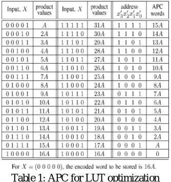
[image:4.612.223.390.261.438.2]For simplicity of presentation, we assume both X and A to be positive integers. The product words for different values of X for L = 5 are shown in Table I. It may be observed in this table that the input word X on the first column of each row is the two’s complement of that on the third column of the same row. In addition, the sum of product values corresponding to these two input values on the same row is 32A.
Table 1: APC for LUT optimization
The product values on the second and fourth columns of Table 1 therefore have negative mirror symmetry. This behavior of the product words can be used to reduce the LUT size, where, instead of storing U and V only [(V-U)/2] is stored for a pair of input on a given row. The 4-bit LUT addresses and corresponding coded words are listed on the fifth and sixth columns of the table, respectively. Since the representation of the product is derived from the anti-symmetric behavior of the products, we can name it as anti-symmetric product code
1) Modified OMS For LUT Optimization: For the multiplication of any binary word X of size L, with a fixed coefficient A, instead of storing all the 2L possible values of C=A.X, only (2L/2) words corresponding to the odd multiples of A may be stored in the LUT, while all the even multiples of A could be derived by left-shift operations of one of those odd multiples. Based on the above assumptions, the LUT for the multiplication of an L-bit input with a W-bit coefficient could be designed by the following strategy.
A memory unit of [(2L/2) + 1] words of (W+L)-bit width is used to store the product values, where the first (2L/2) words are odd multiples of A and the last word is zero.
A barrel shifter for producing a maximum of (L− 1) left shifts is used to derive all the even multiples of A.
The L-bit input word is mapped to the (L− 1) bit address of the LUT by an address encoder and control bits for the barrel shifter are derived by a control circuit.
B. Memory-Based FIR Filter Using Conventional LUT
LUT-Technology (IJRASET)
©IJRASET: All Rights are Reserved
68
multiplier. Each multiplication node performs the multiplication of an input sample value with the absolute value of a filter coefficient. The AS node adds or subtracts its input from top with or from that of its input from the left when the corresponding filter coefficient is positive or negative respectively. It may be noted here that each of the multiplication nodes performs multiplications of input samples with a fixed positive number. This feature can be utilized to implement the multiplications by an LUT that stores the results of multiplications of all possible input values with the multiplying coefficient of a node as unsigned numbers. The multiplication of an L-bit unsigned input with W-bit magnitude part of fixed filter weight, to be performed by each of the multiplication-nodes of the DFG, can be implemented conventionally by a dual-port memory consisting of words of (W+L) bit width. Each of the nodes of the DFG along with a neighbouring delay element can be mapped to an add-subtract (AS) cell. A fully pipelined structure for N-tap FIR filter for input word length L=8 is derived accordingly from the DFG. It consists of N memory-units for conventional LUT-based multiplication, along with (N-1) AS cells and a delay register. All the 8 bits of current input sample x (n) are fed to all the multipliers in parallel as a pair of 4-bit addresses X1 andX2 and the structure of the LUT-multiplier
Structure of each LUT-multiplier consisting of 16 words of (W+4)-bit width) and a shift-add (SA) cell. The SA cell shifts its right-input to left by four bitlocations and adds the shifted value with its other right-input to produce a (W+8)-bit output. The shift operation in the shiftadd cells is hardwired with the adders, so that no additional shifters are required. The outputs of the multipliers are fed to the pipeline of AS cells in parallel. Each AS cell performs exactly the same function as that of the AS node of the DFG.It consists of either an adder or a subtracteddepending on whether the corresponding filter weight h(n) is positive ornegative respectively.
C. Structure of the Nor-Cell
The RESET bit is fed as one of the inputs of all those NOR gates, and the other input lines of (W+4) NOR gates of NORcell are fed with (W+4) bits of LUT output in parallel.
Technology (IJRASET)
©IJRASET: All Rights are Reserved
69
It consists of two stages of 2-to-1 line bit-level multiplexors with inverted output, where each of the two stages involves (W+4) number of 2-input AND-OR-INVERT (AOI) gates. The control-bits and are fed to the AOI gates of stage-1 and stage-2 of the barrel-shifter respectively. Since each stage of the AOI gates perform inverted multiplexing, after two stages of inverted multiplexing, outputs with desired number of shifts are produced by the barrel shifter in (the usual) un-inverted form.
D. CSD-Canonical Sign Digit Algorithm (CSD)
The CSD representation is radix-2 signed digit system with the digit set {1, 0,1}, where _1 denotes - 1.Given a constant, the corresponding CSD representation is unique and has two properties, the first is that the number of nonzero digits is minimal and the second is that the product of two adjacent digits is zero. i.e two nonzero digits are not adjacent. An Encoding a binary number such that it contains the fewest number of nonzero bits is called Canonical Sign Digit. A CSD representation is a kind of sum of signed power of two representations. Unlike binary numbers, that is expressed using only 0 and 1,but the CSD representation and the SPT representation use 0, 1 and -1.
Ex: 71*X = 10001112*X = X ≪6 + X ≪2 + X ≪1 + X (shift/add operation) --- (3.1)
10001112*X = 100100-1*X = X ≪6 + X ≪3 −X (CSD) --- (3.2)
With Ci € {-1, 1, 0}, where (- denotes -1). It is signed digit number system that minimizes the number of nonzero digits.
It can reduce the number of partial product additions in a hardware multiplier. They are successful in implementing multipliers with less complexity. Since the complexity of the multipliers is typically estimated through the number of non-zero elements, which can be reduced by using signed digit numbers. Adjacent CSD digits are never both zero. For negative numbers, the numbers of non-zero digits is less for the CSD Representation than the 2’sComplement representation. The CSD numbers has the minimum number of non-zero digits and no consecutive nonzero digits. The CSD Representation has fewer nonzero digits than the normal binary expression. Now the multipliers in the digital filters are realized with shifters, adders and subtractions. The use of CSD expression can reduce the number of adders and sub tractors for example, the normal binary representation would need 3 adders, as 15 is represented as 11112. The number of adders and sub tractors is less than the number of non-zero digits by 1.The CSD Multiplier is based on shifts and adds (or subtracts) instead of conventional multipliers. This results in the area reduction of multiplier of the digital filters.
E. Reconfigurable CSD Fir Filter Design
Technology (IJRASET)
©IJRASET: All Rights are Reserved
70
techniques in the integer domain, we can obtain a CSD FIR filter with less degradation.
Figure.5.Multiplier Block Using Add And Shift
III. RESULTS AND DISCUSSION
We have implemented the FIR filter using proposed LUTmultiplier and LUT-multiplier based transposed form FIR filter both of order four using Xilinx tool
IV. CONCLUSION
Technology (IJRASET)
©IJRASET: All Rights are Reserved
71
this filter system has a good performance, the filter speed is higher and the resource occupation is fewer. Compared with the traditional filters, this filter is more popular in digital signal processing. This work can be extended by increasing the order of filter for accurate outputs i.e., in some applications like medicine more accurate filters are used.
REFERENCES
[1] J. G. Proakis, D. G. Manolakis, ―Digital Signal Processing:Principles, Algorithms and Applicationsǁ. Upper SaddleRiver, NJ: Prentice- Hall, 1996.
[2] G. Mirchandani, R. L. Zinser Jr., and J. B. Evans, ―A new adaptive noise cancellation scheme in the presence of crosstalk [speech signals],ǁ IEEE Trans. Circuits Syst. II, Analog. Digit. Signal Process. vol. 39, no. 10, pp. 681–694, Oct. 1995.
[3] D. Xu and J. Chiu, ―Design of a high-order FIR digital filtering and variable gain ranging seismic data acquisition system,ǁ in Proc. IEEE Southeastcon’93, Apr. 1993, p. 6.
[4] H. H. Dam, A. Cantoni, K. L. Teo, and S. Nordholm, ―FIR variable digital filter with signed power-of-two coefficients,ǁ IEEE Trans. Circuits Syst. I, Reg. Papers, vol. 54, no. 6, pp. 1348–1357, Jun. 2007.
[5] R. Mahesh and A. P. Vinod, ―A new common sub expression elimination algorithm for realizing low-complexity higher order digital filters,ǁ IEEE Trans. Computer-Aided Ded. Integr. Circuits Syst., vol. 27, no. 2, pp. 217–229, Feb. 2008.
[6] K. K. Parhi, VLSI Digital Signal Procesing Systems: Design and Implementation. New York: Wiley, 1999.
[7] H. H. Kha, H. D. Tuan, B.-N. Vo, and T. Q. Nguyen, ―Symmetric orthogonal complex-valued filter bank design by semidefinite programming,ǁ IEEE Trans. Signal Process., vol. 55, no. 9, pp. 4405–4414, Sep. 2007.
[8] D. F. Chiper, M. N. S. Swamy, M. O. Ahmad, and T. Stouraitis, ―Systolic algorithms and a memory-based design approach for a unified architecture for the computation of DCT/DST/IDCT/IDST,ǁ IEEE Trans. Circuits Syst. I, Reg. Papers, vol. 52, no. 6, pp. 1125–1137, Jun. 2005.
[9] J.-I. Guo, C.-M. Liu, and C.-W. Jen, ―The efficient memory-based VLSI array design for DFT and DCT,ǁ IEEE Trans. Circuits Syst. II, Analog Digit. Signal Process. vol. 39, no. 10, pp. 723–733, Oct. 1992.
[10] P. K. Meher, ―Memory-based hardware for resource-constrained digital signal processing systems,ǁ in Proc. 6th Int. Conf. ICICS, Dec. 2007, pp. 1–4. [11] H.-R. Lee, C.-W. Jen and C.-M. Liu, ―On the design automation of the memory-based VLSI architectures for FIR filters,ǁ IEEE Trans. Consum. Electron.vol.
39, no. 3, pp. 619–629, Aug. 1993.
[12] D. F. Chiper, M. N. S. Swamy, M. O. Ahmad, and T. Stouraitis, ―A systolic array architecture for the discrete sine transform,ǁ IEEE Trans. Signal Process., vol. 50, no. 9, pp. 2347–2354, Sep. 2002.
[13] H.-C. Chen, J.-I. Guo, T.-S. Chang and C.-W. Jen, ―A memory-efficient realization of cyclic convolution and its application to discrete cosine transform,ǁIEEE Trans. Circuits Syst. Video Technol., vol. 15, no. 3, pp. 445–453, Mar. 2005
[14] P. K. Meher, ―Systolic designs for DCT using a low-complexity concurrent convolutional formulation,ǁ IEEE Trans. Circuits Syst. Video Technol., vol. 16, no. 9, pp. 1041–1050, Sep. 2006.