Technology (IJRASET)
©IJRASET: All Rights are Reserved
531
Analysis and Simulation of E-Shape Microstrip
Patch Antenna for Wideband Applications
Sachin Kumar1, Ajay Kumar2, Pooja Nain3 1
Department of Electronics and Communication Engineering, World College of Tech. & Mangt., Haryana,India
2
Department of Electronics and Communication Engineering, World College of Tech. & Mangt., Haryana,India
3
Department of Electronics and Communication Engineering, CBS Group of Institutions, Haryana,India
Abstract— This paper presents the design and simulation of E-shape microstrip patch antenna with wideband operating frequency for wireless application. The shape will provide the broad bandwidth which is required in various application like remote sensing, biomedical application, mobile radio, satellite communication etc. The antenna design is an improvement from Previous research and it is simulated using HFSS (High Frequency Structure Simulator) version 11 software. Coaxial feed or probe feed technique is used in the experiment. Parametric study was included to determine affect of design towards the antenna performance. The performance of the designed antenna was analyzed in term of bandwidth, gain, return loss, VSWR, and radiation pattern. The design was optimized to meet the best possible result. Substrate used was air which has a dielectric constant of 1.0006. The results show the wideband antenna is able to operate from 8.80 GHz to 13.49 GHz frequency band with optimum frequency at 8.73 GHz.
Index Terms — E-shape microstrip patch antenna, HFSS (High Frequency Structure Simulator) version 11 software, wideband.
I. INTRODUCTION
[image:2.612.190.425.554.690.2]Microstrip patch antenna is a key building in wireless communication and Global Positioning system since it was first demonstrate in 1886 by Heinrich Hertz and its practical application by Guglielmo Marconi in 1901. Future trend in communication design is towards compact devices. Microstrip patch antenna have been well known for its advantages such as light weight, low fabrication cost, mechanically robust when mounted on rigid surfaces and capability of dual and triple frequency operations all these features, attract many researchers to investigate the performance of parch antenna in various ways. However, narrow bandwidth came as the major disadvantage for this type of antenna.Several techniques have been applied to overcome this problem such as increasing the substrate thickness, introducing parasitic elements i.e. co-planar or stack configuration, or modifying the patch’s shape itself. Modifying patch’s shape includes designing an E-shaped patch antennas or a U-slot patch antenna.U-slot microstrip antenna provides bandwidth up to 30% while E-shaped patch antenna can increases bandwidth above 30% compared to a regular rectangular patch antenna. Comparing both designs, the E-shaped is much simpler to construct by only adjusting length, width and position of slots. In this paper, a wideband single patch antenna is proposed as in Figure 1. The main objective of this paper is to optimize the base design in to obtain higher bandwidth. This single patch antenna operates at voltage standing wave ratio of less than 2 (VSWR < 2). Theoretical simulation and optimization are performed using HFSS (High Frequency Structure Simulator) version 11 software.
Technology (IJRASET)
©IJRASET: All Rights are Reserved
532
II. DESIGN METHODOLOGY OF RADIATING ELEMENT
Recently there have been numerous methods of enhancing the bandwidth of an antenna for example modifying the probe feed, using multiple resonances, using folded patch feed, or using the slotted radiating element.The U shape slot in the radiating element tends to have wideband characteristics. It also suggests that a U shape slot introduces the capacitive component in the input impedance to counteract the inductive component of the probe. Also to compensate the increasing inductive effect due to the slots, thickness of the substrate is increased.
As we know that as thickness increases the bandwidth increases accordingly. The input impedance of about 42% is achieved. The slots making it to look alike inverted E shape; it demonstrated a bandwidth enhancement by 30 %.In this design an air-filled or foam
has been essential to realize broadband characteristics. This design uses substrate material with relative permittivity (ε) of 1.0006 i.e. Air and the patch shape is the combination of inverted E and inverted U.
A. Simulation Setup
The antenna’s resonant properties were predicted and optimized using High Structure simulation software Ansoft version 11. The design procedure begins with determining the length, width and the type of dielectric substance for the given operating frequency as shown in flow diagram Fig.2. Then using the measurements obtained above simulation has been setup for the basic rectangular microstrip antenna and the parameters are optimized for the best impedance matching. Furthermore two parallel slots are incorporated and optimized such that it closely resembles E shape; this increases the gain of the antenna. After that two more parallel slots and one perpendicular slots are incorporated and optimized such that it closely resembles U shape.Then dielectric substrate od dielectric constant of 1.0006 introduces to decrease the size of the antenna and to further enhance the bandwidth. At last the probe feeding is introduced for attaining a required bandwidth, resonating frequency and gain value. The proposed design methodology of the antenna is given in Fig.(2).
Technology (IJRASET)
©IJRASET: All Rights are Reserved
533
B. Geometry of the antenna
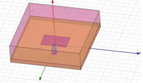
The geometry of the designed antenna is shown in the Fig.3.The antenna is made of a single patch on top, one layers of dielectric (air) and a vertical probe connected from ground to the upper patch.
Fig.3Design geometry of E shaped patch antenna
The main E shaped patch has Wa x La dimension while the outer patch has Wb x Lb dimension. The antenna is fed by a SMA connector positioned at the center arm. The center of probe is positioned at (Wc/2,Lf). The width and length of the microstrip antenna are determine as follows
Where νo is the free-space velocity of light.
Where the dimensions of the patch along its length have been extended on each end by a distance ΔL, which is a function of the
effective dielectric constant εreff and the widthto- height ratio (W/h), and the normalized extension of the length, is
The actual length of the patch (L) can be determine as
Technology (IJRASET)
©IJRASET: All Rights are Reserved
534
obtain wider bandwidth and higher gain.
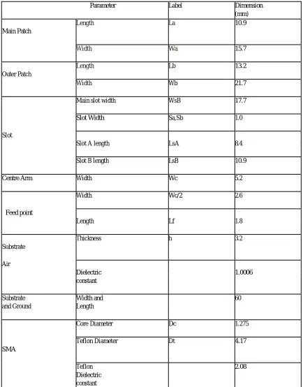
[image:5.612.88.522.154.708.2]Air gap was used as substrate and infinite ground was assumed. This paper design a finite set of ground dimension which is defined by Wg x Lg. SMA connector design is according to specification in using Teflon of dielectric constant = 2.08. The default value of this antenna design is shown in Table 1.
Table 1: Default microstrip patch antenna specifications
Parameter Label Dimension
(mm)
Length La 10.9
Main Patch
Width Wa 15.7
Length Lb 13.2
Outer Patch
Width Wb 21.7
Main slot width WsB 17.7
Slot Width Sa,Sb 1.0
Slot
Slot A length LsA 8.4
Slot B length LsB 10.9
Centre Arm Width Wc 5.2
Width Wc/2 2.6
Feed point
Length Lf 1.8
Thickness h 3.2
Substrate
Air
Dielectric 1.0006
constant
Substrate Width and 60
and Ground Length
Core Diameter Dc 1.275
SMA
Teflon Diameter Dt 4.17
Teflon 2.08
Technology (IJRASET)
©IJRASET: All Rights are Reserved
535
III. PARAMETRIC STUDY
The default value of dimension for this antenna is presented in Table 1. Dimension that are kept constant in this paper are
Main Patch, Outer Patch, Substrate’s thickness, LsB and SMA feed. Other parameters are set as variables. Only oneparameter is allowed to change at a time while other variables remain constant as default except ground and substrate that will varied together. All dimension mentioned in graphs are in millimetre (mm).
A. Changing Air Gap with C-Foam PF-2
The microstrip antenna is simulated with C-Foam PF-2 substrate that has a dielectric constant of 1.03 and compared the output with the microstrip antenna which is simulated with Air that has a dielectric constant of 1.0006. The result is shown in Figure 5. Replacing air gap (blue) with C-Foam PF-2 (red) we found that the bandwidth is slightly decreased as compared to air gap(blue) so air gap gives wider bandwidth than foam. The reason to use C-Foam PF-2 is because outer patch in is connected to main patch by switches, but in this paper, no switches will be used, so a substrate is needed to connect outer patch to main patch. As mentioned,
[image:6.612.136.479.278.595.2]dielectricconstant for this foam is 1.03 which is very close to air gap, so that the reference result would not be much difference when using air gap. Using C-Foam PF-2, the frequency band is from 8.74 GHz to 13.36 GHz while when using Air gap, the band is from 8.80 GHz to 13.49 GHz, which create a slightly wider bandwidth.
Fig.5 S11for air and foam substrate
B. Changes in substrate size
Technology (IJRASET)
[image:7.612.155.459.81.322.2]©IJRASET: All Rights are Reserved
536
Fig.6 S11 of various size of substrate
C. Changes in Centre Arm Width (Wc)
[image:7.612.185.427.407.598.2]Figure 7 shows the S11 parameter when Wc varied from 4.2 mm to 6.2 mm by 0.5 mm increment. As the width increases, the 1st and 2nd resonant frequency shifted to lower frequency and the magnitude of S11 decreases. The opposite occur at the 3rd resonant frequency where the frequency does not seem to change very much, but magnitude of S11 increases as the width of centre arm increases.
Fig.7 S11 of various size of Wc
D. Changes in Slot Length (LsA)
Technology (IJRASET)
[image:8.612.155.463.72.253.2]©IJRASET: All Rights are Reserved
537
Fig.8 S11 of various size of LsA
E. Changes in Main Slot Width (WsB)
[image:8.612.168.450.311.482.2]WsB is varied from 15.7 mm to 19.7 mm with increment of 1 mm. The result shown in Figure 9 shows a pattern when WsB is varied Low cut-off frequency is virtually the same for all values. The upper cut-off decreases as WsB increases. It can be said WsB influence the bandwidth of other parameters are kept constant.
Fig.9 S11of various size of WsB
F. Changes in Slot Width (Sa,Sb)
Slot widths, Sa and Sb is varied from 0.5 mm to 2mm, with increment of 0.5 mm. For Sa, almost similar pattern can be seen in Figure 10. Magnitude for S11 at 1st resonant frequency decreases as Sa Increase while the opposite happen at 3rd resonant frequency, when magnitude of S11 increases as Sa decreases. S11 magnitude is very low when Sa= 2 mm.
[image:8.612.162.460.585.709.2]In Figure 11, when Sb varied all value show a similar pattern. Magnitude for S11 at 1st and 3rd resonant frequency decreases as Sb Increase. Very low S11 magnitude occurred when Sb = 2 mm.
Technology (IJRASET)
[image:9.612.163.455.79.331.2]©IJRASET: All Rights are Reserved
538
Fig.11 S11of various size of Sb
IV. RESULTS AND DISCUSSION
[image:9.612.102.509.397.661.2]Antenna is optimized based on the results obtained in section III. The aim of optimization is to obtain better gain and bandwidth than Figure 5 and Figure 6. We select only that specification where we get better results after the parametric studies .The varied parameters specification after optimization is shown in Table 2.
Table 2. Optimization Parameters
Parameter Label Dimension (mm)
Main slot width WsB 15.7
Slot Slot A Width Sa 2
Slot B Width Sb 0.6
Slot A length LsA 8.8
Centre Arm Width Wc 4.7
Ground Width Wg 60
Length Lg 60
A. Improvement in Bandwidth, Gain,S11 and VSWR
Technology (IJRASET)
[image:10.612.164.444.80.218.2]©IJRASET: All Rights are Reserved
539
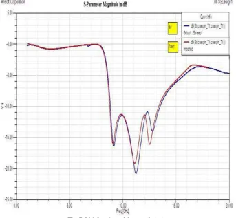
Fig.12 Comparison of three antenna design
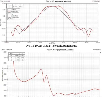
The gain measure for microstrip antenna is 7.6731dB as shown in Figure 6.19.A perfectly matched antenna would have a VSWR of 1:1. This ratio indicates how much power is reflected back or transferred into a cable. VSWR is closely related to S11 the line
impedance set in this paper is 50 Ω. Figure 6.20 shows the VSWR for default specification, the lowest VSWR value is 0.1812dB.
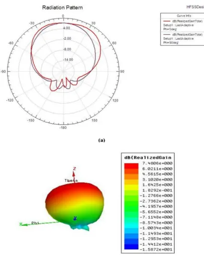
Figure 13(a) and (b) show the radiation pattern for the antenna at 8.73 GHz. HPBW is the angular separation which the magnitude of the radiation pattern from the peak of the main beam decreases by 50% or -3 dB. HPBW (angle) is 70˚ for Optimum
Frequency of 8.73 GHz.. Table 6.12 Shows the Values for radiation parameter for each frequency.
Fig. 13(a) Gain Display for optimized microstrip
[image:10.612.110.504.330.706.2]Technology (IJRASET)
©IJRASET: All Rights are Reserved
540
B. Radiation Pattern of Optimized Antenna
Figure 14(a) and (b) show the radiation pattern for the antenna at 8.73 GHz. HPBW is the angular separation which the magnitude of the radiation pattern from the peak of the main beam decreases by 50% or -3 dB. HPBW (angle) is 70˚ for Optimum Frequency
of 8.73.
[image:11.612.102.512.147.670.2]Technology (IJRASET)
©IJRASET: All Rights are Reserved
541
Table 3: Values for radiation parameter for each frequency
V. CONCLUSION
In this paper, an E-shaped wideband microstrip patch antenna using Air substrate has been designed, simulated, optimized and analyzed using HFSS (High Frequency Structure Simulator) software version 11. A parametric study is presented with the results showing that the antenna can be operated at 8.80 GHz up to 13.49 GHz frequency band. Thisresult is an improvement when compared to the original.
REFERENCES
[1] Ge, Y.; Esselle, K.P.; Bird, T.S.; , "E-shaped patch antennas for highspeed wireless networks," Antennas and Propagation, IEEE Transactions on , vol.52, no.12, pp. 3213- 3219, Dec. 2004
[2] B.-K. Ang and B.-K. Chung, "A wideband e-shaped microstrip patch antenna for 5 - 6 GHz wireless communications," Progress In Electromagnetics Research, Vol. 75, 397-407, 2007.
[3] Yang, F.; Xue-Xia Zhang; Xiaoning Ye; Rahmat-Samii, Y.; "Wide-band E-shaped patch antennas for wireless communications," Antennas and Propagation, IEEE Transactions on , vol.49, no.7, pp.1094-1100, Jul 2001
[4] Hadian, A.M.; Hassani, H.R.; , "Wideband Rectangular Microstrip Patch Antenna with U-Slot," Antennas and Propagation, 2007. EuCAP 2007. The Second European Conference on , vol., no., pp.1-5, 11-16 Nov. 2007
[5] Vedaprabhu, B.; Vinoy, K.J.; , "A double U-slot patch antenna with dual Wideband characteristics," Communications (NCC), 2010 National Conference on , vol., no., pp.1-4, 29-31 Jan. 2010
[6] Weigand, S.; Huff, G.H.; Pan, K.H.; Bernhard, J.T.; , "Analysis and design of broad-band single-layer rectangular U-slot microstrip patch antennas," Antennas and Propagation, IEEE Transactions on , vol.51, no.3, pp. 457- 468, March 2003
[7] Verma, M.K.; Verma, S.; Dhubkarya, D.C.; , "Analysis and designing of E-shape microstrip patch antenna for the wireless communication systems," Emerging Trends in Electronic and Photonic Devices & Systems, 2009. ELECTRO '09. International Conference on , vol., no., pp.324-327, 22-24 Dec. 2009
[8] Wang, B.-Z.; Xiao, S.; Wang, J.; , "Reconfigurable patch-antenna design for wideband wireless communication systems," Microwaves, Antennas & Propagation, IET , vol.1, no.2, pp.414-419, April 2007