International Journal of Emerging Technology and Advanced Engineering
Website: www.ijetae.com (ISSN 2250-2459, ISO 9001:2008 Certified Journal, Volume 6, Issue 5, May 2016)202
Design & Analysis of Digital Circuits Using ECRL and
Stacking Technique
Komal
1, Kapil Mangla
2, Shalini Kashyap
31ECE, Satya College of Engineering & Technology, Palwal,India 2,3A.P.,ECE, Satya College of Engineering & Technology, Palwal,India
1
[email protected] 2[email protected]
Abstract— In today's world low power issues have become a major important factor in modern VLSI design. Low power has blown out as a principle theme in current era of electronic industries. Power dissipation has become a vital consideration as performance and area for VLSI chip design the power consumption of integrated circuits increases with large number of transistors and higher operating frequency. In this paper, Circuits are implemented by using different techniques and results are compared such as average power consumed, delay, no. of transistors. The designing of schematic and simulation of these logics done on Tanner EDA v13.1. From results it is found that power consumption of Stacking is less as compare to ECRL and CMOS.
Keywords— Low power, Conventional CMOS, ECRL, Stacking, Tanner EDA tool, T-Spice.
I. INTRODUCTION
Power consumption plays an important role in the present day VLSI technology. As many of the present day electronic devices are portable, they need more battery backup which can be achieved only with the low power consumption circuits that are internally designed in them. So energy efficiency has become main concern in the portable equipments to get better performance with less power dissipation. As the power dissipation in a device increases then extra circuitry is necessary to cool the device and to protect the device from thermal breakdown which also results in increase of total area of the device. In order to overcome these problems the power dissipation of the circuit is to be reduced by adopting different low power techniques. The less the power dissipation ,the more efficient the circuit will be[12] .From the past few decades CMOS technology plays a dominant role in designing low
power consuming devices. The power consumption in conventional CMOS circuit is due to switching activity of the devices from one state to another state and due to the charging and discharging of load capacitor at the output node. But reducing the values of these parameters may degrade the performance of the device. So an efficient low power technique other than CMOS is needed that has less power dissipation compared to CMOS which can be done by using adiabatic technique[11].
The present paper focuses on novel energy efficient techniques called adiabatic logic and Stacking which is based on energy recycle and recovery principle. In the stacking technique the leakage of power is reduced by breaking down existing transistors in to two half size transistors. By which its reverse bias induces which results to prevent leakage. The Stacking technique is more useful as compared to ECRL technique. Since power consumption is also less in stacking technique.
II. POWER ANALYSIS OF CMOSCIRCUITS
The power consumption of digital CMOS circuits is generally considered in terms of three components[13]:
The dynamic power component, related to the
charging and discharging of the load capacitance at the gate output.
The short-circuit power component. During the
transition of the output line (of a CMOS gate) from one voltage level to the other, there is a period of time when both the PMOS and the NMOS transistors are on, thus creating a path from Vdd to ground.
The static power component, due to leakage, that
International Journal of Emerging Technology and Advanced Engineering
Website: www.ijetae.com (ISSN 2250-2459, ISO 9001:2008 Certified Journal, Volume 6, Issue 5, May 2016)203
source-drain leakage attributed to both tunneling and sub-threshold conduction.
Power can be estimated at a number of levels of details. The main levels include:
Circuit Level Power Estimation, using a circuit simulator such as SPICE.
Static Power Estimation does not use the input vectors, but may use the input statistics.
Logic Level Power Estimation, often linked to
logic simulation.
III. ADIABATIC TECHNIQUE
Adiabatic logic has a different logic style which helps in the reduction of the power dissipation of the circuit. The present paper explains basic gates using adiabatic techniques[12].
A. ECRL Technology
ECRL stands for efficient charge recovery logic. It has a latch of cross-coupled PMOSFETS . The basic construction of ECRL is matched with cascade voltage switch logic (CVSL).It has two PMOSFETS which are connected back to back like out/ is gives the input to m2 and out gives the input to m1. For logic operation, F n-tree and F/ n-tree blocks are used[5]. A ramp or pulse voltage is applied to the circuit and in ECRL, it will be recycled back to the main supply. Two outputs out and out/ are used to describe the condition of ECRL operation. An oscillations are occurred due to the PMOSFETS switches works in pre-charge and recoverable states[3].There is irreversible condition because of thresholding of PMOSFETS in pre-charge and recoverable states. When ramp voltage and threshold voltage are equal then PMOSFETS will be in off condition. Fig. 1 show its structure[4].
Figure. 1 CMOS Circuit using Adiabatic ECRL Technique.
IV. STACKING TECHNIQUE FOR POWER REDUCTION
One technique for leakage power reduction is the stack approach, which forces a stack effect by breaking down an existing transistor into two half size transistors [4]. Fig.2 shows its structure[2]. When the two transistors are turned off together, induced reverse bias between the two transistors results in sub threshold leakage current reduction. However, divided transistors increase delay significantly and could limit the usefulness of the approach[2].
Figure. 2 CMOS Circuit using Stacking Approach.
V. PROPOSED WORK
[image:2.612.376.523.271.455.2]A. INVERTER
[image:2.612.71.264.552.706.2]International Journal of Emerging Technology and Advanced Engineering
Website: www.ijetae.com (ISSN 2250-2459, ISO 9001:2008 Certified Journal, Volume 6, Issue 5, May 2016)204
Figure.4 Waveform for voltage of Conventional CMOS Inverter
Figure.5 Waveform for power of Conventional CMOS Inverter
Figure.6 Circuit for Inverter using Stacking technique
Figure.7Waveform for voltage of Inverter using Stacking technique
Figure.8 Waveform for power of Inverter using Stacking technique.
International Journal of Emerging Technology and Advanced Engineering
Website: www.ijetae.com (ISSN 2250-2459, ISO 9001:2008 Certified Journal, Volume 6, Issue 5, May 2016) [image:4.612.319.562.109.310.2]205
[image:4.612.47.291.112.306.2]Figure.10 Waveform for voltage of Adiabatic ECRL Inverter
Figure.11 Waveform for power of Adiabatic ECRL Inverter
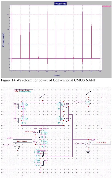
B. NAND
Figure.12 Circuit for Conventional CMOS NAND
[image:4.612.322.561.321.700.2]Figure.13 Waveform for voltage of Conventional CMOS NAND.
Figure.14 Waveform for power of Conventional CMOS NAND
[image:4.612.47.289.329.486.2] [image:4.612.48.285.508.696.2]International Journal of Emerging Technology and Advanced Engineering
Website: www.ijetae.com (ISSN 2250-2459, ISO 9001:2008 Certified Journal, Volume 6, Issue 5, May 2016) [image:5.612.321.561.108.495.2]206
[image:5.612.49.286.112.303.2]Figure.16 Waveform for voltage of NAND using Stacking technique.
Figure.17 Waveform for power of NAND using Stacking technique.
Figure. 18 Circuit for Adiabatic ECRL NAND
[image:5.612.46.286.336.576.2]Figure.19 Waveform for voltage of Adiabatic ECRL NAND
Figure.20 Waveform for power of Adiabatic ECRL NAND
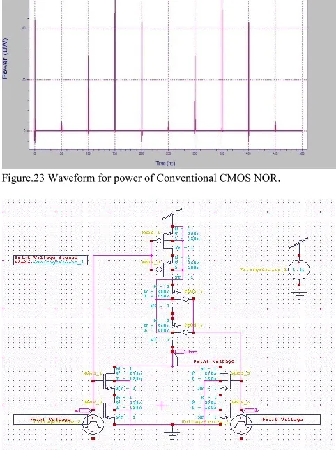
[image:5.612.46.288.445.696.2]C. NOR
[image:5.612.323.562.515.703.2]International Journal of Emerging Technology and Advanced Engineering
Website: www.ijetae.com (ISSN 2250-2459, ISO 9001:2008 Certified Journal, Volume 6, Issue 5, May 2016) [image:6.612.48.290.114.301.2]207
[image:6.612.323.565.124.296.2]Figure.22 Waveform for voltage of Conventional CMOS NOR .
Figure.23 Waveform for power of Conventional CMOS NOR.
Figure. 24 Circuit for NOR using Stacking technique.
[image:6.612.323.563.319.689.2]Figure.25 Waveform for voltage of NOR using Stacking technique
Figure.26 Waveform for power of NOR using Stacking technique
[image:6.612.47.288.357.680.2]International Journal of Emerging Technology and Advanced Engineering
Website: www.ijetae.com (ISSN 2250-2459, ISO 9001:2008 Certified Journal, Volume 6, Issue 5, May 2016) [image:7.612.47.288.113.475.2]208
[image:7.612.320.567.115.499.2]Figure.28 Waveform for voltage of Adiabatic ECRL NOR
Figure.29 Waveform for power of Adiabatic ECRL NOR.
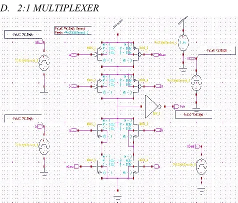
D. 2:1 MULTIPLEXER
Figure. 30 Circuit for Conventional CMOS Multiplexer.
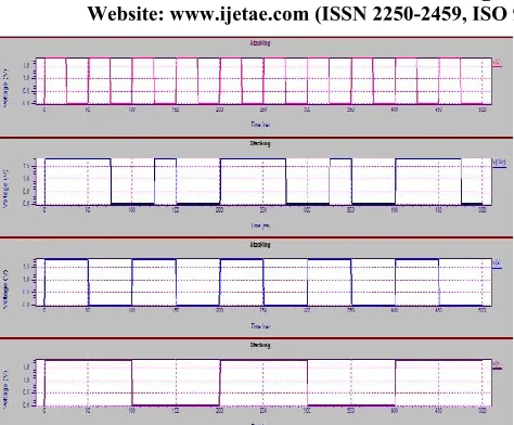
[image:7.612.322.565.330.693.2]Figure.31 Waveform for voltage of Conventional CMOS Multiplexer.
Figure.32 Waveform for power of Conventional CMOS Multiplexer.
[image:7.612.48.286.492.695.2]International Journal of Emerging Technology and Advanced Engineering
Website: www.ijetae.com (ISSN 2250-2459, ISO 9001:2008 Certified Journal, Volume 6, Issue 5, May 2016) [image:8.612.320.564.113.318.2]209
[image:8.612.49.286.118.314.2]Figure.34 Waveform for voltage of Multiplexer using Stacking technique
Figure.35 Waveform for power of Multiplexer using Stacking technique.
Figure. 36 Circuit for Adiabatic ECRL Multiplexer.
[image:8.612.324.564.332.489.2]Figure.37 Waveform for voltage of Adiabatic ECRL Multiplexer.
Figure.38 Waveform for power of Adiabatic ECRL Multiplexer.
VI. RESULTS
This section deals with the comparision of the CMOS logic style with the Adiabatic ECRL and STACKING technique in terms of no. of transistors, average Power consumed and Delay. The results were simulated using TSPICE tanner tool in 180nm technology .
TABLEI
CMOS INVERTER RESULTS
Power Reduction Techniques
No. of Transistors
Average Power Consumed
(In Microwatts)
Average Delay (In Nanoseconds)
Conventional 2 0.729 0.713
ECRL 4 0.351 0.0987
[image:8.612.47.287.337.497.2] [image:8.612.49.283.507.688.2] [image:8.612.323.563.620.716.2]International Journal of Emerging Technology and Advanced Engineering
Website: www.ijetae.com (ISSN 2250-2459, ISO 9001:2008 Certified Journal, Volume 6, Issue 5, May 2016)210
TABLEIII
CMOS NAND GATE RESULTS
Power Reduction Techniques No. of Transistors Average Power Consumed (In Microwatts) Average Delay (In Nanoseconds)
Conventional 4 0.954 0.761
ECRL 6 0.501 0.098
Stacking 8 0.415 0.925
TABLEIIIII CMOS NOR GATE RESULTS
Power Reduction Techniques No. of Transistors Average Power Consumed (In Microwatts) Average Delay (In Nanoseconds)
Conventional 4 0.482 0.507
ECRL 6 0.295 0.137
Stacking 8 0.18 0.637
TABLEIV
CMOS 2:1MULTIPLEXER RESULTS
Power Reduction Techniques
No. of
Transistors Average Power Consumed (In Microwatts) Average Delay (In Nanoseconds)
Conventional 10 2.324 0.182
ECRL 10 1.074 0.057
Stacking 18 0.834 0.383
Figure.39:Graph For No. of Transistor, Average Power consumed and Average Delay For Inverter.
Figure.40:Graph For No. of Transistor, Average Power consumed and Average Delay For NAND.
Fig.41:Graph For No. of Transistor, Average Power consumed and Average Delay For NOR.
International Journal of Emerging Technology and Advanced Engineering
Website: www.ijetae.com (ISSN 2250-2459, ISO 9001:2008 Certified Journal, Volume 6, Issue 5, May 2016)211
References
[1] W. C. Athas, L.J. Svensson, J.G. Koller, N.Tzartzanis, and E. Chou, ―Low power digital systems based on adiabatic-switching principles,‖IEEE Trans. VLSI Systems, vol. 2, no. 4, pp. 398-407, Dec. 1994.
[2] Neha Goyal , Renu Singla, Puneet Goyal, ―study & analysis of universal gates using stacking low power technique:, International journal of computer science & Information technologies, vol 6(3), 2014, pp 4200- 4204.
[3] A.P. CHANDRAKASAN AND R.W. BRODERSEN, LOW- POWER CMOS digital design, Kluwer Academic, Norwell, May 1995
[4] Debaprasad Das ‖VLSI Design‖ published by Oxford University Press 2010.
[5] W.C. ATHAS, J.G.KOLLER, L.SVENSSON, ―An Energy Efficient CMOS Line Driver using Adiabatic Switching‖, Fourth Great Lakes symposium on VLSI, California, March 2005.
[6] B. Dilip, p. Surya prasad & r. S. G. Bhavani ―Leakage power reduction in CMOS circuits using Leakage control transistor technique in nanoscale Technology‖ in International Journal of Electronics Signals and Systems (IJESS) ISSN: 2231- 5969, Vol-2 Iss-1, 2012.
[7] Y. Moon and D.K. Jeong, ―An efficient charge recovery logic circuit,‖ IEEE J. Solid-State Circuits, vol. 31, no. 4, pp. 514–522, Apr. 1996.
[8] Renu Singla, Puneet Goyal, Neha Singla, ―Comparative study and analysis of universal gates for minimizing power and delay using lector techniques‖ IJARCS, vol. 5(5), may – june-2014, pp 29-33
[9] P. K. Sharma, B. Bhargava, S. Akashe―Reduction of Leakage Power in Digital Logic Circuits Using Stacking Technique in 45 Nanometer Regime‖ International Journal of Electrical, Computer, Energetic, Electronic and Communication Engineering Vol:7, No:1, 2013
[10] C. HU, ―Future CMOS Scaling and Reliability,‖ Proceedings IEEE, Vol. 81, No. 05, pp. 682-689, February 2004.
[11] B.Dilli Kumar, M.Bharathi,‖Design of Energy Efficient Arithmetic Circuits using Charge Recovery Adiabatic Logic‖, International Journal of Engineering Trends & Technology Vol. 4 Issue 1-2013
[12] B.Dilli Kumar, T. Muni Reddy,‖A Novel Implementation of 2x2 Bit Square for low power applications‖, IOSR-JVSP Volume 2, Issue 5, (May-Jun.2013)
![Fig.2 shows its structure[2]. When the two transistors are](https://thumb-us.123doks.com/thumbv2/123dok_us/8692121.877401/2.612.376.523.271.455/fig-shows-structure-transistors.webp)