N A N O E X P R E S S
Open Access
Optimal Silicon Doping Layers of Quantum
Barriers in the Growth Sequence Forming
Soft Confinement Potential of Eight-Period
In
0.2
Ga
0.8
N/GaN Quantum Wells of Blue
LEDs
Hsiang-Chen Wang
1, Meng-Chu Chen
2, Yen-Sheng Lin
3, Ming-Yen Lu
4, Kuang-I Lin
5and Yung-Chen Cheng
6*Abstract
The features of eight-period In0.2Ga0.8N/GaN quantum wells (QWs) with silicon (Si) doping in the first two to five quantum barriers (QBs) in the growth sequence of blue light-emitting diodes (LEDs) are explored. Epilayers of QWs’ structures are grown on 20 pairs of In0.02Ga0.98N/GaN superlattice acting as strain relief layers (SRLs) on patterned sapphire substrates (PSSs) by a low-pressure metal-organic chemical vapor deposition (LP-MOCVD) system. Temperature-dependent photoluminescence (PL) spectra, current versus voltage (I-V) curves, light output power versus injection current (L-I) curves, and images of high-resolution transmission electron microscopy (HRTEM) of epilayers are measured. The consequences show that QWs with four Si-doped QBs have larger carrier localization energy (41 meV), lower turn-on (3.27 V) and breakdown (−6.77 V) voltages, and higher output power of light of blue LEDs at higher injection current than other samples. Low barrier height of QBs in a four-Si-doped QB sample results in soft confinement potential of QWs and lower turn-on and breakdown voltages of the diode. HRTEM images give the evidence that this sample has relatively diffusive interfaces of QWs. Uniform spread of carriers among eight QWs and superior localization of carriers in each well are responsible for the enhancement of light output power, in particular, for high injection current in the four-Si-doped QB sample. The results demonstrate that four QBs of eight In0.2Ga0.8N/GaN QWs with Si doping not only reduce the quantum-confined Stark effect (QCSE) but also improve the distribution and localization of carriers in QWs for better optical performance of blue LEDs.
Keywords:InGaN/GaN quantum wells, Silicon doping, Blue light-emitting diodes, Soft confinement potential, Localization of carriers, Quantum-confined Stark effect
Background
Silicon (Si) doping in GaN quantum barriers (QBs) can kindle Coulomb screening of polarization field and cause suppression of quantum-confined Stark effect (QCSE) in InGaN/GaN quantum wells (QWs). Radiative recombina-tions of excitons in InGaN/GaN QWs can be enhanced considerably through Si-doped QBs [1–4]. Compositional fluctuations of indium (In) and spinodal phase separation occur in ternary alloy InGaN on account of the inherent
solid-phase miscibility gap of GaN and InN. The forma-tion of In-rich clusters could act as strong carrier localiza-tions, preventing the traps of nonradiative recombination centers (NRCs) and facilitating the radiative recombin-ation of excitons in InGaN/GaN QWs [5–10]. Fluctuation of indium composition in InGaN/GaN QWs has a signifi-cant impact on the behaviors of devices, e.g., internal quantum efficiency (IQE), external quantum efficiency (EQE), and current-voltage characteristics. Indium fluctu-ation in InGaN/GaN QWs should be taken into account to have better explanations of the performance of devices [11]. InGaN/GaN QWs with Si-doped QBs have shown the properties of modifications of material nanostructure * Correspondence:[email protected]
6Department of Materials Science, National University of Tainan, Tainan 70005, Taiwan
Full list of author information is available at the end of the article
and formations of nanoscale islands due to the spiral growth of the QW layers [12], promotion of the thermal stability of InGaN/GaN QWs [13], improvement of light output power and electrostatic discharge (ESD) behaviors of the LED as the doping concentration in QBs is increased [14], easy blocking of hole carrier transport leading to recombination of excitons at the wells between p-type GaN (p-GaN) and the doped barriers [15], etc.
The favorable periods and thickness of InGaN/GaN QWs for high brightness and high EQE under high injec-tion current (above several tens of mA) of blue LEDs are reported [16–18]. In the reports, nine periods of InGaN/ GaN QWs grown on patterned sapphire substrates (PSSs) show a significant improvement of light emission power and droop properties of EQE [16]. The best optical and electrical performances of blue LEDs are demonstrated if the active region consists of 12 periods of InGaN/GaN QWs at the injection current 42 A/cm2 [17]. Apparent reduction of EQE droop and enhancement of IQE are demonstrated for the thickness of QB reduced from 24.5 to 9.1 nm in the simulation results of InGaN/GaN LEDs [18]. Si doping in proper thickness and numbers of QBs in InGaN/GaN QWs is crucial for further promotion of brightness and efficiency of InGaN blue LEDs operating at high injection current. In this report, we present the optical, electrical, and material characteristics of eight-period In0.2Ga0.8N/GaN QWs with first two to five QBs in
the growth sequence possessing Si doping of blue LEDs. The results give a deeper insight into the mechanisms of carrier localization, confinement potential, and QCSE of QWs on luminescence behaviors of blue LEDs under high injection current.
Experimental Methods
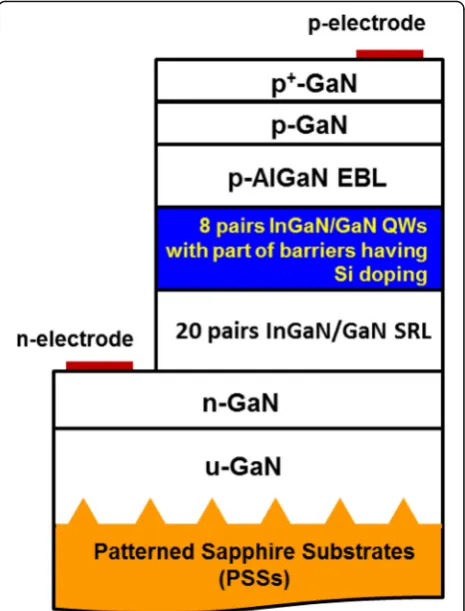
Figure 1 depicts the schematic illustration of material layer structures of blue LED samples. Epilayers are deposited by a horizontal reactor of a low-pressure metal-organic chem-ical vapor deposition (LP-MOCVD) system on (0001)-orientation (c-plane) PSSs. The diameter, height, and inter-val of regular pyramid structures on PSSs are 2, 1.5, and 1μm, respectively. PSSs have a thickness of 3μm and are preheated at 1150 °C in the ambience of hydrogen before the growth of epilayers. Trimethylgallium (TMGa), trimethy-lindium (TMIn), trimethylaluminum (TMAl), and gaseous NH3are utilized as vapor-phase precursors of elemental
gal-lium (Ga), In, aluminum (Al), and nitrogen (N), respectively. Silane (SiH4) and bis-cyclopentadienyl magnesium (Cp2Mg)
are precursors of the dopant Si and magnesium (Mg) in the n- and p-type substances, respectively. Carrier gases of pre-cursors are the mixture of hydrogen (H2) and nitrogen (N2)
with the ratio 1:1 which is chemically nonreactive.
Undoped GaN (u-GaN) buffer layer and then Si-doped n-type GaN (n-GaN) with a thickness of 3 and 3.3 μm are grown upon PSSs. The doping concentration of
n-GaN is 1019 cm−3. Twenty pairs of In0.02Ga0.98N/GaN
superlattice with the thickness 2/2 nm are subsequently deposited on n-GaN. It plays the role of strain relief layers (SRLs), which is used to reduce the extension of strain from the epilayers on PSSs.
Active layers of blue LEDs contain eight-period In0.2Ga0.8N/GaN QWs. The thicknesses of QW and QB
are 2.5 and 8 nm with the growth temperature 750 and 900 °C, respectively. Si doping with a concentration around 3 × 1017 cm−3in the first two, three, four, and five QBs in the growth sequence is named as samples A, B, C, and D, respectively. p-type Al0.16Ga0.84N electron
blocking layer (EBL) has a thickness of 20 nm and is grown at 950 °C with Mg doping. p-GaN window layer and p+-GaN contact layer are grown at 950 °C with a thickness of 100 and 20 nm, and doping concentrations are 1019and 1020cm−3.
Epilayers are etched selectively to the n-GaN layer by an inductively coupled plasma (ICP) system to form mesa structure LED. The indium tin oxide (ITO) trans-parent contact layer (TCL) is deposited onto the p+-GaN surface by an electron beam evaporator. Chromium/plat-inum/gold (Cr/Pt/Au) multi-metal contact electrode layers are subsequently evaporated onto the p+-GaN and
[image:2.595.306.539.88.394.2]n-GaN layers for good ohmic contact. LED wafers are lapped and polished down to about 120 μm for chip dicing. Standard mesa-type LED devices with a square chip size of 1 mm2are produced.
The current versus voltage (I-V) curves and the light output power (Pout) versus injection current (L-I) curves
from 20 to 300 mA at room temperature (RT) of diodes are measured. Temperature-dependent photolumines-cence (PL) spectra of eight-period In0.2Ga0.8N/GaN
QWs are examined. The excitation light source of PL is He-Cd laser (325 nm) with the average power 45 mW. The high-resolution transmission electron microscopy (HRTEM) images are taken from an EM-3000F field emission transmission electron microscope (FE-TEM) with an accelerating voltage of 300 kV and resolution of 0.14 nm.
Results and Discussion
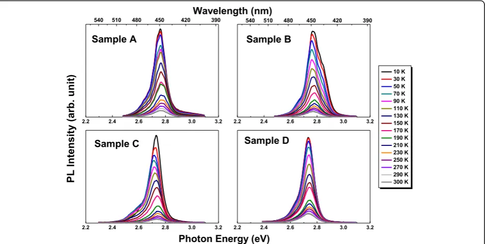
Figure 2 plots the PL spectra of samples at various tem-peratures from 10 to 300 K. The monotonic decrease of PL peak intensity with the increase of temperature can be observed. This is originated from the raise of nonra-diative recombination process with the increase of temperature. All PL spectral profiles are fitted by Gauss-ian lineshape functions to find the variations of peak maximum energy with temperature as demonstrated in Fig. 3. The emission peak maximum energy of PL for the undoped In0.2Ga0.8N/GaN QWs is 2.68 eV at room
temperature. This means that PL peak energies of sam-ples with first two to five QBs having Si doping exhibit a blue shift when it is compared with the undoped one.
The first two to five QBs with Si doping can lower the QCSE in QWs effectively. It should be pointed out that the uses of PSSs and SRLs in the structures of epilayers can reduce the part of piezoelectric (PZ) field as well as QCSE in In0.2Ga0.8N/GaN QWs.
In Fig. 3, variations of PL peak maximum energy versus temperature that exhibit S-shape curves of all samples can be shown. The S-shape curves display initial red then blue and then red shift with the increase of temperature. This behavior is attributed to temperature-dependent collective luminescence of strong localized excitons in QWs. The Varshni empirical equation shown below can be used to fit the range of blue to red shift of the S-shape variations [19–21].
Egð Þ ¼T Egð Þ−0 αT 2
T−β
ð Þ−
σ2
kBT ð
1Þ
whereEg(0),α, β, andσ are the fitting parameters.Eg(0)
[image:3.595.62.539.88.328.2]nondegenerate carrier distribution and Gaussian-like localized density of state. Strong carrier localization is a crucial aspect in realizing the raise of radiative recom-bination and IQE in InGaN QWs due to the improve-ment of the overlap between electron and hole wave functions. The Varshni equation is not applicable in the range of red shift of PL peak energy at low temperature, owing to the strong degeneracy in carrier distribution. The best fitting results of samples are illustrated in thick
and black solid curves in Fig.3. The localization energy of samples A, B, C, and D is 24, 28, 41, and 13 meV, respectively. Sample C possesses the largest localization energy,σ(41 meV). Carrier localization in the QWs with four Si-doped QBs is stronger than the others. The smallest localization energy (σ) happens in sample D with the value 13 meV.
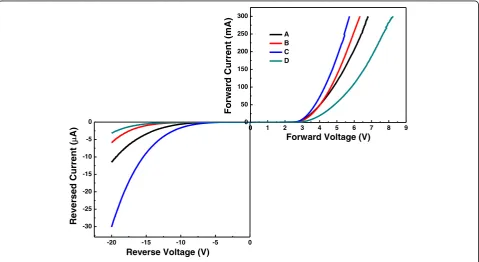
Current-voltage (I-V) characteristics under forward and reverse bias of blue LEDs are demonstrated in Fig. 4.
-20 -15 -10 -5 0
-30 -25 -20 -15 -10 -5 0
d
e
sr
e
v
e
Rt
n
er
r
u
C(
A
)
Reverse Voltage (V)
0 1 2 3 4 5 6 7 8 9
0 50 100 150 200 250 300
Forward Current (mA)
Forward Voltage (V)
A B C D
Fig. 4Current-voltage (I-V) curves under forward and reversed biases of diodes
0 50 100 150 200 250 300
2.72 2.73 2.74 2.75 2.76 2.77 2.78
Sample A Sample B Sample C Sample D
Photon Energy (eV)
Temperature (K)
456 454 452 450 448 446
Wavelength (nm)
[image:4.595.58.539.88.294.2] [image:4.595.59.539.456.718.2]In this figure, the turn-on voltages for samples A, B, C, and D are 3.41, 3.47, 3.27, and 4.03 V at the forward current 20 mA, respectively. The breakdown voltages for samples A, B, C, and D are−8.85,−9.99,−6.77, and− 11.55 V at the reverse current 1μA, respectively. Sample C has the smallest turn-on and breakdown voltages. Sample D has the largest turn-on and breakdown volt-ages. Accordingly, lower barrier height of QBs is sug-gested in sample C. Soft (smooth) confining potential of QWs is expected in the sample with the first four QBs having Si doping. Soft confinement potential profile im-plies that conduction and valence band offsets of QWs are not taken as sharp step functions, i.e., not rectangu-lar confining potential. Smooth confining potentials can suppress the Auger recombination to a great extent and prevent accumulation of plenty carriers in the first sev-eral wells in the injection direction of InGaN/GaN QWs [22–24]. Smooth confining potential can also be made through a linear decrease of In composition along the
growth direction of InGaN/GaN QWs. This can have better spread of carriers among QWs and transportation of holes which results in improvement of quick drop of EQE and light output power [25–30].
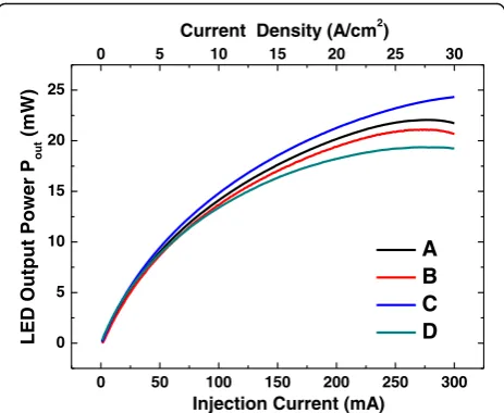
Figure 5 shows the measurements of light output power (Pout) of LEDs versus injection current (L-I) curve
from 0 to 300 mA by a chip tester. The increase of the Pout with the raise of injection current ofL-Icurves can
be observed. The highest and the lowest Pout for high
injection current are shown in samples C and D, respect-ively. Saturations ofPoutat the injection current 300 mA
are shown in all samples except for sample C. Saturation effect of Pout is referred to the current overflowing the
QWs. The less current overflowing the QWs takes place in the soft confinement potential of QWs and strong carrier localization inside the QW sample. Better spread of carriers among eight QWs and strong radiative recombination of carriers inside QWs are displayed in the sample with four QBs containing Si doping.
The dark-field, bright-field, and enlarged bright-field images of cross-sectional high-resolution transmission electron microscope (HRTEM) of samples are shown in Figs. 6, 7, and 8. In Fig. 6, bright and dark contrasts cor-respond to InGaN and GaN epilayers. Eight periods of QWs and 20 pairs of superlattices can be observed. In Fig. 7, dark contrast variations represent the fluctuations of local In content and formation of indium-rich clusters in QWs [31–34]. Indium-rich clusters act as relatively deep localized states of carriers leading to high radiative excitonic recombination. Lattice distortion and stacking fault defects are noted around these indium-rich clus-ters, indicating that the strain energy partly relaxed in the InGaN layer as shown in the zoom in picture of the red square in Fig. 8a. Compared with the enlarged bright-field images, more diffusive (not abrupt) inter-faces of QWs in samples C and D are seen as exhibited in Fig. 8c, d. The agent comes from the well-known in-terdiffusion of In and Ga atoms at the well/barrier inter-face. Very weak confinement and carrier localization of
Fig. 6Dark field images of the samples.aSample A.bSample B.cSample C.dSample D
0 50 100 150 200 250 300
0 5 10 15 20 25
Current Density (A/cm2)
Injection Current (mA)
P
r
e
w
o
P
t
u
pt
u
O
D
E
L
out
)
W
m(
A B C D
0 5 10 15 20 25 30
Fig. 5Light output power (Pout) versus injection current (L-I) curves
[image:5.595.58.290.87.277.2] [image:5.595.58.542.567.714.2]QWs occurred in sample D which is in accordance with the worst optoelectronic behavior of this sample. In the images, threading dislocations (TDs) do not form in all samples. NRCs occur primarily at TD sites. Better qual-ity of epilayers is shown in these samples as expected due to the employing of PSSs and SRLs [35–37]. Four QBs with Si doping in eight-period QWs are the favor-able condition to modify the confinement potential to attain soft confinement potential of InGaN/GaN QWs, leading to the best optoelectronic performance of blue LED.
Conclusions
Temperature-dependent PL spectra, I-V curves, L-I curves, and HRTEM images of blue LEDs with eight-period In0.2Ga0.8N/GaN QWs having the first two to five
QBs in the deposition sequence containing Si doping
were investigated. The results demonstrate that the sam-ple with the first four QBs containing Si doping has rela-tively lower barrier height and larger localization energy of carriers which is evidenced by diffusive interfaces of QWs in HRTEM images. Soft confinement potential of QWs accompanied with stronger carrier localization inside QWs gives rise to a more uniform distribution of carrier among eight QWs and higher radiative recombin-ation of carriers inside QWs in this sample. A decrease of Auger processes and leakage of carriers as well as an increase of radiative recombination of QWs occurred in blue LEDs with four Si-doped QBs under high injection current. The results provide optimal conditions of QBs with Si doping through the analyses of the effects of car-rier localization, confinement potential, PZ field, and material nanostructures on the luminescence properties of In0.2Ga0.8N/GaN QWs of blue LEDs.
[image:6.595.62.540.87.247.2] [image:6.595.56.541.482.713.2]Abbreviations
Al:Aluminum; Cp2Mg: Bis-cyclopentadienyl magnesium; EBL: Electron blocking layer;
EQE: External quantum efficiency; FE-TEM: Field emission transmission electron microscope; Ga: Gallium; HRTEM: High-resolution transmission electron microscopy; ICP: Inductively coupled plasma; In: Indium; IQE: Internal quantum efficiency; ITO: Indium tin oxide;I-V: Current versus voltage;L-I: Light output power versus injection current; LP-MOCVD: Low-pressure metal-organic chemical vapor depos-ition; Mg: Magnesium; N: Nitrogen; n-GaN: n-type GaN; NRCs: Nonradiative recombination centers; PL: Photoluminescence; PSSs: Patterned sapphire substrates; PZ: Piezoelectric; QBs: Quantum barriers; QCSE: Quantum-confined Stark effect; QWs: Quantum wells; RT: Room temperature; Si: Silicon; SiH4: Silane; SRLs: Strain relief
layers; TCL: Transparent contact layer; TMAl: Trimethylaluminum; TMGa: Trimethylgallium; TMIn: Trimethylindium; u-GaN: Undoped GaN
Acknowledgements
This work is correlated with the Grant Proposal no. 105WFA0F50144 submitted to the Ministry of Science and Technology and the revised Grant Proposal supported by the National University of Tainan with project no. AB105-213.
Funding
This funding is supported by the Ministry of Science and Technology under the Grants MOST 104-2221-E-194-054, 105-2923-E-194-003-MY3, and 105-2112-M-194-005.
Authors’Contributions
HCW contributed the data of optical measurements. MCC provided the samples and data of electrical measurements of the devices. YSL participated in the discussion of the cross-sectional HRTEM images. MYL provided the data of measurements of HRTEM. KIL participated in the discussion of the results of optical measurements. YCC analyzed the data and wrote the manuscript. All authors read and approved the final manuscript.
Competing Interests
The authors declare that they have no competing interests.
Publisher’s Note
Springer Nature remains neutral with regard to jurisdictional claims in published maps and institutional affiliations.
Author details
1
Graduate Institute of Opto-Mechatronics, National Chung Cheng University, Chiayi 62102, Taiwan.2Department of Applied Science, National Taitung University, Taitung 950, Taiwan.3Department of Electronic Engineering, I-Shou University, Kaohsiung 84001, Taiwan.4Department of Materials Science and Engineering, National Tsing Hua University, Hsinchu 30013, Taiwan.5Center for Micro/Nano Science and Technology, National Cheng Kung University, Tainan 70101, Taiwan.6Department of Materials Science, National University of Tainan, Tainan 70005, Taiwan.
Received: 27 July 2017 Accepted: 30 October 2017
References
1. Deguchi T, Shikanai A, Torii K, Sota T, Chichibu S, Nakamura S (1998) Luminescence spectra from InGaN multiquantum wells heavily doped with Si. Appl Phys Lett 72:3329–3331
2. Dalfors J, Bergman JP, Holtz PO, Sernelius BE, Monemar B, Amano H, Akasaki I (1999) Optical properties of doped InGaN/GaN multiquantum-well structures. Appl Phys Lett 74:3299–3301
3. Zhang Z-H, Tan ST, Ju Z, Liu W, Ji Y, Kyaw Z, Dikme Y, Sun XW, Demir HV (2013) On the effect of step-doped quantum barriers in InGaN/GaN light emitting diodes. J Display Technol 9:226–233
4. Griffiths JT, Zhang S, Rouet-Leduc B, Fu WY, Bao A, Zhu D, Wallis DJ, How kins A, Boyd I, Stowe D, Kappers MJ, Humphreys CJ, Oliver RA (2015) Nano cathodoluminescence reveals mitigation of the stark shift in InGaN quantum wells by Si doping. Nano Lett 15:7639–7643
5. O’Donnell KP, Martin RW, Middleton PG (1999) Origin of luminescence from InGaN diodes. Phys Rev Lett 82(1):237–240
6. Chen H, Feenstra RM, Northrup JE, Zywietz T, Neugebauer J (2000) Spontaneous formation of indium-rich nanostructures on InGaN (0001) surfaces. Phys Rev Lett 85:1902–1905
7. Kazlauskas K, Tamulaitis G, Pobedinskas P,Žukauskas A, Springis M, Huang C-F, Cheng Y-C, Yang CC (2005) Exciton hopping in InxGa1−xN multiple
quantum wells. Phys Rev B 71:085306-1–085306-5
8. Cheng Y-C, Lin E-C, Wu C-M, Yang CC, Yang J-R, Rosenauer A, Ma K-J, Shi S-C, Chen LS-C, Pan C-S-C, Chyi J-I (2004) Nanostructures and carrier localization behaviors of green-luminescence InGaN/GaN quantum-well structures of various silicon-doping conditions. Appl Phys Lett 84:2506–2508 9. Cooke M (2013) Bridging the amber-green gap and white LEDs. Semicond
Today-Compounds Advanced Silicon 7:82–88
10. Biswas D, Mistry A, Bera PP (2017) Evidence of the formation of small nanostructures in the growth of InGaN/GaN multi-quantum wells. Optik 130:1358–1361
11. Wu Y-R, Shivaraman R, Wang K-C, Speck JS (2012) Analyzing the physical properties of InGaN multiple quantum well light emitting diodes from nano scale structure. Appl Phys Lett 101:083505-1–083505-4
12. Uchida K, Tang T, Goto S, Mishima T, Niwa A, Gotoh J (1999) Spiral growth of InGaN/InGaN quantum wells due to Si doping in the barrier layers. Appl Phys Lett 74:1153–1155
13. Kusakabe K, Hara T, Ohkawa K (2005) Impurity doping effect on thermal stability of InGaN/GaN multiple quantum-well structures. J Appl Phys 97:043503-1–043503-3
14. Park E-H, Kang DNH, Ferguson IT, Jeon S-K, Park J-S, Yoo T-K (2007) The effect of silicon doping in the selected barrier on the electroluminescence of InGaN/GaN multiquantum well light emitting diode. Appl Phys Lett 90:031102-1–031102-3
15. Chiang TH, Chiou YZ, Chang SJ, Lin TK, Chang SP (2011) Effect of silicon doped quantum barriers on nitride-based light emitting diodes. J Electrochem Soc 158:H836–H839
16. Tanaka S, Zhao Y, Koslow I, Pan C-C, Chen H-T, Sonoda J, DenBaars SP, Nakamura S (2011) Droop improvement in high current range on PSS-LEDs. Electron Lett 47:335–336
17. Xia CS, Li ZMS, Li ZQ, Sheng Y, Zhang ZH, Lu W, Cheng LW (2012) Optimal number of quantum wells for blue InGaN/GaN light-emitting diodes. Appl Phys Lett 100:263504-1–263504-4
18. Lin G-B, Kim D-Y, Shan Q, Cho J, Schubert EF, Shim H, Sone C, Kim JK (2013) Effect of quantum barrier thickness in the multiple-quantum-well active region of GaInN/GaN light-emitting diodes. IEEE Photon J 5:1600207–1600207 19. Wang H, Ji Z, Qu S, Wang G, Jiang Y, Liu B, Xu X, Mino H (2012) Influence of
excitation power and temperature on photoluminescence in InGaN/GaN multiple quantum wells. Opt Express 20:3932–3940
20. Lu T, Ma Z, Du C, Fang Y, Wu H, Jiang Y, Wang L, Dai L, Jia H, Liu W, Chen H (2014) Temperature-dependent photoluminescence in light-emitting diodes. Sci Rep 4:1–7
21. Li Z-Y, Lo M-H, Chiu C-H, Lin P-C, Lu T-C, Kuo H-C, Wang S-C (2009) Carrier localization degree of In0.2Ga0.8N/GaN multiple quantum wells grown on
vicinal sapphire substrates. J Appl Phys 105:013103-1–013103-7 22. Vaxenburg R, Lifshitz E, AlL E (2013) Suppression of Auger-stimulated
efficiency droop in nitride-based light emitting diodes. Appl Phys Lett 102:031120-1–031120-5
23. Yoo Y-S, Na J-H, Son SJ, Cho Y-H (2016) Effective suppression of efficiency droop in GaN-based light-emitting diodes: role of significant reduction of carrier density and built-in field. Sci Rep 6:1–9
24. Tsai C-L, Wu W-C (2014) Effects of asymmetric quantum wells on the structural and optical properties of InGaN-based light-emitting diodes. Materials 7:3758–3771
25. Chang C-Y, Li H, Lu T-C (2014) High efficiency InGaN/GaN light emitting diodes with asymmetric triangular multiple quantum wells. Appl Phys Lett 104:091111-1–091111-5
26. Wang CH, Chang SP, Ku PH, Li JC, Lan YP, Lin CC, Yang HC, Kuo HC, Lu TC, Wang SC, Chang CY (2011) Hole transport improvement in InGaN/GaN light-emitting diodes by graded-composition multiple quantum barriers. Appl Phys Lett 99:171106-1–171106-3
27. Zhang Z-H, Liu W, Ju Z, Tan ST, Ji Y, Kyaw Z, Zhang X, Wang L, Sun XW, Demir HV (2014) InGaN/GaN multiple-quantum-well light-emitting diodes with a grading InN composition suppressing the Auger recombination. Appl Phys Lett 105:033506-1–033506-5
28. McBride PM, Yan Q, Van de Walle CG (2014) Effects of In profile on simulations of InGaN/GaN multi-quantum-well light-emitting diodes. Appl Phys Lett 105:083507-1–083507-1
30. Arif RA, Ee Y-K, Tansu N (2007) Polarization engineering via staggered InGaN quantum wells for radiative efficiency enhancement of light emitting diodes. Appl Phys Lett 91:091110-1–091110-3
31. Lin Y-S, Ma KJ, Hsu C, Feng S-W, Cheng Y-C, Liao C-C, Yang CC, Chou CC, Lee C-M, Chyi J-I (2000) Dependence of composition fluctuation on indium content in InGaN/GaN multiple quantum wells. Appl Phys Lett 77:2988–2990 32. Lin Y-S, Ma K-J, Hsu C, Chung Y-Y, Liu C-W, Feng S-W, Cheng Y-C, Yang CC,
Mao M-H, Chuang H-W, Kuo C-T, Tsang J-S, Weirich TE (2002) Quasiregular quantum-dot-like structure formation with postgrowth thermal annealing of InGaN/GaN quantum wells. Appl Phys Lett 80:2571–2573
33. Huang Y-S, Feng S-W, Weng Y-H, Chen Y-S, Kuo C-T, Lu M-Y, Cheng Y-C, Hsieh Y-P, Wang H-C (2017) Nanostructure analysis of InGaN/GaN QWs based on semi-polar face GaN nanorods. Opt Mater Express. 7:320–328 34. Chen Y-S, Liao C-H, Kuo C-T, Tsiang RC-C, Wang H-C (2014) Indium droplet
formation in InGaN thin films with single and double heterojunctions prepared by MOCVD. Nanoscale Res Lett 9:1–12
35. Wang W-K, Wuu D-S, Lin S-H, Han P, Horng R-H, Hsu T-C, Huo DT-C, Jou M-J, Yu Y-H, Lin A (2005) Efficiency improvement of near-ultraviolet InGaN LEDs using patterned sapphire substrates. IEEE J Quant Electron 41:1403–1409 36. Gao H, Yan F, Zhang Y, Li J, Zeng Y, Wang G (2008) Enhancement of the
light output power of InGaN/GaN light-emitting diodes grown on pyramidal patterned sapphire substrates in the micro- and nanoscale. J Appl Phys 103:014314-1–014314-5