Designing and Implementation of Charge
Pump for Fast-Locking and Low-Power PLL
Nitesh Pareek, Rahul Moud
Research Scholar, M. Tech . (VLSI), Geetanjali Institute of Technical Studies, Udaipur, Rajasthan, India
Assistant Professor, Department of EC, Geetanjali Institute of Technical Studies, Udaipur, Rajasthan, India
ABSTRACT : This design of wide band VCO used in PLL system which is suitable for wide range of application. PLL’s with high speed, low noise and wide tuning range are preferred . Ring oscillators consist of odd number of inverter stages in order to avoid latch up and we have considered 5 stage current starved VCO with tuning range from 431.68MHz –1.5GHz . We have considered one more VCO design using Operational Transconductance Amplifier (OTA) tuning range from 271.2MHz –3.1GHz consist of OTA stage ,inverter stage and Biasing circuits . The circuits are simulated at schematic level and layout level using180nm technology with supply voltage 5 voltage
I. INTRODUCTION
PLL is used to recover a signal from a noisy communication channel, generate stable frequencies or distribute clock timing pulses in microprocessors. The PLL based frequency synthesizer plays a very significant role in direct frequency modulator, frequency demodulator and the regeneration of the carrier from the input signal in the wireless communications. PLL is used for clock and data recovery circuit in the broadband data communication network, which is used to recover the data from the NRZ clock and data re-timed decision.
II. PHASE LOCK LOOP DESIGN
BASIC PLL CIRCUIT
A PLL is a feedback system that compares the output phase with the input phase. The comparison is performed by a ‘phase comparator’ or ‘phase detector’. The basic elements of a Phase locked Loop (PLL) are a Phase detector (PD), Low Pass Filter (LPF) and a voltage controlled oscillator (VCO) in a feedback loop.
Fig. 1: Basic Block Diagram of PLL
ISSN(Online): 2320-9801
ISSN (Print) : 2320-9798
I
nternational
J
ournal of
I
nnovative
R
esearch in
C
omputer
and
C
ommunication
E
ngineering
(A High Impact Factor, Monthly, Peer Reviewed Journal)
Website: www.ijircce.com
Vol. 7, Issue 1, January 2019
PHASE FREQUENCY DETECTOR CIRCUIT DESIGN
For the periodic signal it is possible to merge the phase and frequency detector, such that it can detect both phase and frequency. It is called as phase-frequency detector (PFD).
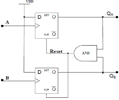
The PFD is shown in figure 3.2
Fig. 2 Implementation of PFD
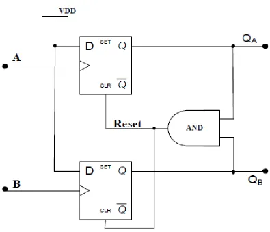
PHASE FREQUENCY DETECTOR CIRCUIT DESIGN
For the periodic signal it is possible to merge the phase and frequency detector, such that it can detect both phase and frequency. It is called as phase-frequency detector (PFD).
Fig. 3 Implementation of PFD
Design of Phase Lock Loop
These design criteria are often I conflicts and improving one particular aspect of the design constrains the other. So each sub block of PLL has been designed in this chapter to satisfy all these properties.
Thus the basic block of PLL consists of five fundamental blocks, namely, PFD, CP, LPF, VCO and FD. The proposed PLL is designed to achieve the following properties
. Reduced locking time . Low power dissipation . Delay reduction
. Transistor Count
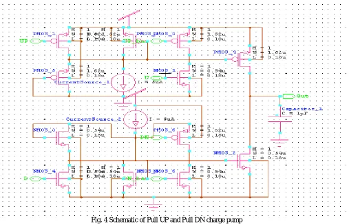
Pull up and Pull down Charge Pump
ISSN(Online): 2320-9801
ISSN (Print) : 2320-9798
I
nternational
J
ournal of
I
nnovative
R
esearch in
C
omputer
and
C
ommunication
E
ngineering
(A High Impact Factor, Monthly, Peer Reviewed Journal)
Website: www.ijircce.com
Vol. 7, Issue 1, January 2019
are negligible. At this condition the capacitor holds the previous charge and the output voltage remains at its original value. When the UP signal is again switched from low to high then P4 and N1 will be ON. These P4 and N1 are used to reduce the charging time delay of P3. When DN signal is high, then the pull down network is ON and capacitor C will be discharged. When they are both ON, they operate in the saturation region.
Fig. 4 Schematic of Pull UP and Pull DN charge pump
The current mirror structure is used in this circuit, so current mismatch is minimized. This charge pump also has increased output voltage but the power dissipation is again high. So another charge pump is designed to achieve both the properties of increased output voltage with low power dissipation.
III. SIMULATION RESULT
2Charge Pump
Fig.5Simulation waveform of current mirror charge pump
IV. CONCLUSION
The present work studies the important charge pump and PLL architectures and their performance. In this project, a high speed CMOS sense amplifier for PLL application has been designed and simulated using the 180 nm CMOS technology. Thus this project simulates and analyses some of the major reported sense amplifier architectures for fast locking and less transistor count compared with the design of PLL using charge pump.
REFERENCES
[1]. Jyoti Gupta, Ankur Sangal Hemlata Verma “High Speed CMOS Charge Pump Circuit for PLL Applications using 90nm CMOS Technology” World Congress on Information and Communication Technologies IEEE pp.346-349, 2011.
[2]. Silin Liu and Yin Shi, “ Fast Locking and High Accurate Current Matching Phase-Locked Loop” IEEE pp. 1136-1139,2008.
[3]. Abishek Mann, Amit Karalkar, Lili He, and Morris Jones, “The Design of A Low-Power Low-Noise Phase Lock Loop” IEEE pp. 528-531,2010. [4]. Seoncheol Kim and Youngsik Kim, “A Fractional-N PLL Frequency Synthesizer Design” IEEE pp. 84-87,2005.
[5]. Kun-Seok Lee, Byeong-Ha Park, Han-il Lee, and Min Jong Yoh, “Phase Frequency Detectors for Fast Frequency Acquisition in Zero-dead-zone CPPLLs for Mobile Communication Systems” IEEE pp. 525-528,2003.
[6]. Won - Hyo Lee, Sung - Dae Lee and Jun - Dong Cho, “A High Speed, Low Power Phase-Frequency Detector and Charge-Pump Circuits for High Frequency Phase Locked Loop” IEICE TRANS FUNDAMENTALS,VOL.E82-A,NO,11 NOVEMBER 1999.
[7]. Silin Liu, Zhikun Hao, Heping rna, Ling Yuan, and Yin Shi, “A Fast-Locking Phase-Locked Loop Using a Seven-State Phase Frequency Detector” IEEE -2008.