Comparative Study of Reversible Arithmetic
Logic UnitBased on Programmable Reversible
Gate
Surabhi Goswami, Nishi Pandey, Neelesh Gupta
M. Tech. Scholar, Department of Electronics and Communication, TCST, Bhopal, India Assistant Professor, Department of Electronics and Communication, TCST, Bhopal, India
Head of Dept., Department of Electronics and Communication, TCST, Bhopal, India
ABSTRACT
:
Reversible or information-lossless circuits have applications in digital signal processing, communication, computer graphics and cryptography. Reversibility plays an important role when energy efficient computations are considered. Reversible logic is used to reduce the power dissipation that occurs in classical circuits by preventing the loss of information. This paper comparative study is reversible design for 32-bit, 16-bit, 8-bit, 4-bit 2-bit and 1-bit ALU. These ALU consists of differenttypes of operations i.e. arithmetic and logical operations. The arithmetic operations include addition, subtraction, multiplication, division and the logical operations include NAND, AND, OR, NOT, XNOR, NOR and XOR. All the modules are being designed using the basic reversible gates. Simulation and verification of the design will perform using Xilinx 14.1i with different device family.KEYWORDS: Reversible Gates, Arithmetic Unit (ALU), Garbage Output, Quantum Cost
I. INTRODUCTION
In modern VLSI system power dissipation is very high due to rapid switching of internal signals. The complexity of VLSI circuits increases with each year due to packing more and more logic elements into smaller volumes. Hence power dissipation has become the main area of concern in VLSI design. Reversible logic has its basics from thermodynamics of information processing. According to this, traditional irreversible circuits generate heat due to the loss of information during computation. In order to avoid this information loss the conventional circuits are modeled using reversible logic. Landauer [1961] showed that the circuits designed using irreversible elements dissipate heat due to the loss of information bits [1]. It is proved that the loss of one bit of information results in dissipation of KT*log2 joules of heat energy where K is the Boltzmann constant and T is the temperature at which the operation is performed. Benett [1973] showed that this heat dissipation due to information loss can be avoided if the circuit is designed using reversible logic gates [2]. A gate is considered to be reversible only if for each and every input there is a unique output assignment. Hence there is a one to one mapping between the input and output vectors. A reversible logic gate is an n –input, n- output device indicating that it has same number of inputs and outputs. A circuit that is built from reversible gates is known as reversible logic circuit.
The classical computational process which is irreversible, onebit of information is lost for each logical operation carried out by it. But in 1961, Rolf Landauer’s principle states that for each bit of information.
However, this loss of energy is legible for simple circuits and become significant for complex circuits. In 1973, Bennet showed that there would be no energy dissipation if computations are done in the reversible way [2]. Resultantly, a new paradigm in circuit design evolved with the aim of reducing the entropy increase and energy dissipation [3]. Further, such a logical structure must possess the same number of inputs and outputs and a one-to-one mapping between the input and output states. Any device designed according to the above constraints is known as a reversible logic device [4].
Parameters of Reversible Logic
There are many parameters for determining the complexityand performance of circuits in reversible logic circuit design. The following parameters should be reduced for the efficient reversible circuit design[5].
Gate count (N): This refers to the number of reversible gates used in circuit.
Constant inputs (CI): The number of inputs that are to be maintained constant at either 0 or 1 in order to synthesize the given logical function[5].
Garbage outputs (GO): The number of unused outputs present in a reversible logic circuit. Garbage outputs can’t be avoided as these are essential to achieve reversibility.
Quantum cost (QC): This refers to the cost of the circuit in terms of the cost of a primitive gate.
Gate levels (GL): The number of levels in the circuit which are required to realize the given logic functions[5].
II. LITRATURE SURVEY
A. Deeptha et al. [1],conventional Complementary metal oxide semiconductor circuits (CMOS) dissipate energy in the form of bits of information. This dissipation of energy is in the form of power dissipation and plays a very important role as far as low power design is considered. Today, most digital circuits are being designed using Reversible Logic. Design based on Reversible Logic helps in reducing heat dissipation, allowing nearly energy free computation, allowing higher circuit densities and enabling better testing of faults. In this paper, a novel design for a Reversible 8-bit ALU is proposed. The 8-bit ALU is designed by cascading 1-bit ALUs. The two major units of a 1-bit ALU are the control unit and the adder unit. For the control unit, the Control Output Gate (COG) has been used and for the adder unit the Haghparast and Navi Gate (HNG) has been used.
Kaur Er. Ravijot et al. [2],with the growing advent of VLSI technology, the device size is shrinking and the complexity of the circuit is increasingexponentially. Power dissipation is considered as one of the most important design parameter. Reversible logic is an emerging and promising technology that provides almost zero power dissipation. Power consumption is also considered as an important parameter in digital circuits. In this paper, an efficient fault tolerant 32-bit reversible arithmetic and logic unit is designed and implemented using some parity preserving gates. The proposed design is better in terms of quantum cost and power dissipation. The numbers of garbage outputs are reduced by using them as an arithmetic or logical operation.
Gopal Lenin et al. [3],Reversible logic is gaining importance in areas of CMOS design because of its low power dissipation. The traditional gates like AND, OR, XOR are all irreversible gates. Consider the case of traditional AND gate. It consists of two inputs and one output. As a result, one bit is lost each time a computation is carried out. According to the truth table shown in Fig.1, there are three inputs (1, 0), (0, 1) and (0, 0) that corresponds to an output zero. The input th at is added to an m x n function to make it reversible is known as constant input (CI). All the outputs of a reversible circuit need not be used in the circuit. Those outputs that are not used in the circuit is called as garbage output (GO). The number of garbage output for a particular reversible gate is not fixed.
Morrison Matthew et al. [4], further a new reversible design method that uses the minimum number of garbage outputs is also proposed; the authors in investigate the problem of optimally synthesizing 4-bit reversible circuits using an enhanced bi-directional synthesis approach. Thus, in synthesis of reversible logic circuits, the optimization in terms of number of ancilla input bits and also the delay are not yet addressed except in the recent work which discusses about the post synthesis method for reducing the number of lines (qubits) in the reversible circuits.
Dixit Akankshaet al. [6],reversible or information-lossless circuits have applications in digital signal processing, communication, computer graphics and cryptography. Reversibility plays an important role when energy efficient computations are considered. The arithmetic operations include addition, subtraction, multiplication and the logical operations include NAND, AND, OR, NOT and XOR. All the modules are being designed using the basic reversible gates. The power and delay analysis of the various sub modules is performed and a comparison with the traditional circuits is also carried out.
Viswanath Lekshmi et al. [7],the design of reversible sequential circuits was first introduced in 1988, in which the design of the JK latch was discussed. In the authors introduced reversible latches such as D latch, T latch, etc., along with their corresponding flip-flops. The flip-flops were designed using master-slave strategy in which one reversible latch works as a master latch and the other works as a slave latch.
Morrison M. et. al. [8], The research on reversible logic is expanding towards both design and synthesis. The synthesis of reversible circuits that employ a minimum number of gates and contain no redundant input-output line-pairs (temporary storage channels) is investigated in; Researchers in have used the positive-polarity Reed-Muller expansion of a reversible function to synthesize the function as a network of Toffoli gates; The work in has illustrated the number of garbage outputs that must be added to a multiple output function to make it reversible.
Table 1: Summary of Literature Review
Title Methodology Parameter Scope
Design and Optimization of 8 bit ALU using Reversible Logic
Design 8-bit reversible ALU using COG and HNG Gate
Quantum cost = 26, garbage output = 9
Low power computing
Design and Implementation of Optimized 32-Bit Reversible Arithmetic Logic Unit
Design 32-bit reversible ALU using PFAG and HNG Gate
Quantum cost = 28, ancilla input = 12
CMOS technology
Design and Synthesis of Reversible Arithmetic and Logic Unit (ALU)
Design 16-bit reversible ALU using TSG and HNG Gate
Gate count =27 Delay = 12.64
Low area consumption
Design of a Reversible ALU based on Novel Programmable Reversible Logic Gate Structures
Design 4-bit reversible ALU using Toffoli and HNG Gate
Cost =24 Delay = 11
Less Complexity
Design of Speed, Energy and Power Efficient Reversible Logic Based Vedic ALU for Digital Processors
Design 1-bit reversible ALU using Peres and HNG Gate
Number of slice register = 45, delay = 17.4 ns
Low area and power
Arithmetic & Logic Unit (ALU) Design using Reversible Control Unit
Design 8-bit reversible ALU using PFAG and HNG Gate
Quantum cost= 34, garbage output =14
Nano technology
Design and Analysis of 16 Bit Reversible ALU
Design 16-bit reversible ALU using HNG and PAOG Gate
Gate count =47, ancilla input =12
Digital Circuit system
Design of a Reversible ALU Based on Novel Programmable Reversible Logic Gate Structures
Design 1-bit reversible ALU using DPG and TOG Gate
Delay = 18.3 ns, slice =45, LUTs = 36
Digital Signal Processing
III. PROBLEM FORMULATION
We tackle the problem of finding a basis of literature review residue adder whose adder is large gerbang output and ancilla input to enable targeted computations for a given residue moduli bit size and a given architecture. After going throw the review of various existing work taken in the residue number the following problem formulation:
well as high speed.
Those architectures which involves reversible gate, for example residue signed adder has less regular architecture due to complex routing and requires large silicon area.
IV. REVERSIBLE GATES
Reversible rationale is picking up significance in regions of CMOS configuration in light of its low power dissemination. The conventional entryways like AND, OR, XOR are all irreversible doors. Consider the instance of conventional AND entryway. It comprises of two inputs and one yield. Subsequently, one piece is lost every time a calculation is completed. As indicated by reality table appeared in Fig.1, there are three inputs (1, 0), (0, 1) and (0, 0) that compares to a yield ze ro. Subsequently it is unrealistic to decide interesting information that brought about the yield zero. With a specific end goal to make an entryway reversible extra info and yield lines are added so that a balanced mapping exists between the information and yield. This keeps the loss of data that is fundamental driver of force scattering in irreversible circuits. The info that is added to an m x n capacity to make it reversible is known as steady information (CI). Every one of the yields of a reversible circuit need not be utilized as a part of the circuit [8]. Those yields that are not utilized as a part of the circuit is called as trash yield (GO).The number of garbage output for a particular reversible gate is not fixed. The two main constraints of reversible logic circuit is
Fan out not allowed
Feedbacks or loops not allowed.
o BASIC REVERSIBLE GATES
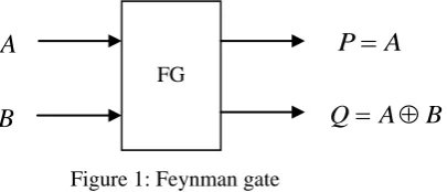
Several reversible logic gates are used in previous design. In figure 1, show the block diagram of two input (A, B) and two output (P, Q) Feynman gate.
In figure 2, show the block diagram of the three inputs (A, B, C) and three output (P, Q, R) Fredkin gate.
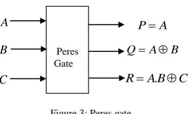
Figure 3 shows the Peres gate. A portion of the 4x4 doors are intended for executing some imperative combinational capacities notwithstanding the fundamental capacities. The vast majority of the aforementioned entryways can be utilized as a part of the outline of reversible adders.
A
P
FG
A
B
Q
A
B
AC
B
A
Q
1
C
B
A
AB
C
A
R
1
FRG
A
P
Figure 1: Feynman gate
The HNG gate, presented in [10], produces the followinglogical output calculations:
A
P
(1)B
Q
(2)C
B
A
R
(3))
(
).
(
A
B
C
AB
D
S
(4)The quantum cost and delay of the HNG is 6. At the point when D = 0, the consistent estimations created on the R and S yields are the required total and complete operations for a full snake. The quantum representation of the HNG is exhibited in Fig. 4.
A new programmable 4x4 reversible logic structure - Peres And-Or(PAOG) gate is presented which produces outputs
A
P
(5)B
A
Q
(6)C
AB
R
(7))
)
((
).
(
AB
C
C
A
B
D
S
(8)Fig. 5 shows the block diagram of the PAOG gate. This gate is an extension of the Peres gate for ALU realization.
B
A
Q
C
B
A
C
B
A
R
.
Peres Gate
A
P
Figure 3: Peres gate
V. PROPOSED METHODOLOGY
The RALU utilizes the DKGgate and BME gate to produce eight logical calculations: transfer A, addition, Sub, XOR, OR, AND, NOT and NAND. The cost and delay calculations are identical to the ALU in figure 6. The RALU has 8 inputs and 8 outputs. The inputs consist of three data inputs (A, B and Cin) and five (S0, S1, S2, S3, S4) lines.
Figure 6: Block Diagram of Proposed Methodology
Figure 7: Flow Diagram of Arithmetic Logic Unit
A
P
B
A
Q
C
AB
R
)
(
)
)
((
C
AB
D
B
A
S
A
B
C
D
PAOG
A reversible logic gate is an n-input n-output logic device with one-to-one mapping. This helps to determine the outputs from the inputs and also the inputs can be uniquely recovered from the outputs.
ALU stands for "Arithmetic Logic Unit." An ALU is an integrated circuit within a CPU or GPU that performs arithmetic and logic operations. Arithmetic instructions include addition, subtraction, and shifting operations, while logic instructions include Boolean comparisons, such as AND, OR, XOR, and NOT operations.
Figure 8: Flow of bit Slice ALU
VI. EXPECTED RESULT
The proposed implementation is programmed (Described) and implemented using VHDL language which is a Hardware Description Language that was developed by the Institute of Electrical and Electronic Engineers (IEEE) as a standard language for describing the structure and behavior of digital electronic systems. It has many features appropriate for describing the behavior of electronic components ranging from simple logic gates to complete microprocessors and custom chips. The resulting VHDL simulation models can then be used as building blocks in larger circuits (using schematics, block diagrams, or system-level VHDL descriptions) for the purpose of simulation.
1. Design 64-bit, 32-bit, 16-bit, 8-bit, 4-bit, 2-bit and 1-bit using different types of reversible gate. 2. Design different types of programmable reversible gate and compared.
3. Design free garbage based architecture using different types of input and compared existing algorithm. 4. Hand calculation of delay and area in reversible arithmetic logic unit in different inputs.
5. All the modules design to different device family i.e. Spartan-3, Virtex-4 and Virtex-7.
VII. CONCLUSION
The 4bit reversible ALU is designed by integrating various sub modules that includes adder/subtract or, and logical unit. The logical unit performs AND, OR, NOR, XOR, NAND. The performance evaluation of the various sub modules are carried out using Modalism 6.5 tools and it was found that the circuits designed using reversible logic showed a reduced delay and power. As a future work more arithmetic and logical function can be used.
Binary Input
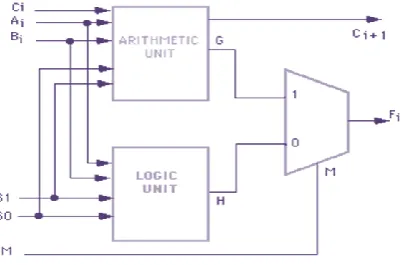
Logic Unit Arithmetic Unit
Control Unit
Selection Line
Parameter
REFERENCES
[1] Deeptha A, DrishikaMuthanna, Dhrithi M, Pratiksha M, B S Kariyappa, “Design and Optimization of 8 bit ALU using Reversible Logic”, IEEE International Conference On Recent Trends In Electronics Information Communication Technology, May 20-21, 2016, India.
[2] Er. Ravijot Kaur and Er. Amandeep Singh Bhandari, “Design and Implementation of Optimized 32-Bit Reversible Arithmetic Logic Unit”, International Journal on Recent and Innovation Trends in Computing and Communication, Volume: 5 Issue: 7, 2016.
[3] Lenin Gopal, Nor Syahira Mohd Mahayadin and Adib Kabir Chowdhury, “Design and Synthesis of Reversible Arithmetic and Logic Unit (ALU)”, 2014 IEEE 2014 International Conference on Computer, Communication, and Control Technology (I4CT 2014), September 2 -4, 2014.
[4] ShefaliMamataj, Biswajit Das, AnurimaRahaman, An Optimized Realization of ALU for 12-Operations by using a Control Unit of reversible gates, International Journal of Advanced Research in Computer Science and Software Engineering, Volume 4, Issue 1, ISSN: 2277 128X, January 2014. [5] Matthew Morrison and NagarajanRanganathan, “Design of a Reversible ALU based on Novel Programmable Reversible Logic Gate Structures”,
2013 IEEE Computer Society Annual Symposium on VLSI.
[6] Mr. Abhishek Gupta, Mr. UtsavMalviya and Prof. Vinod Kapse, “Design of Speed, Energy and Power Efficient Reversible Logic Based Vedic ALU for Digital Processors”, 2012 IEEE.
[7] Akanksha Dixit and VinodKapse, “Arithmetic & Logic Unit (ALU) Design using Reversible Control Unit”, International Journal of Engineering and Innovative Technology (IJEIT) Volume 1, Issue 6, June 2012.
[8] LekshmiViswanath and Ponni. M, “Design and Analysis of 16 Bit Reversible ALU”, IOSR Journal of Computer Engineering (IOSRJCE), Volume 1, Issue 1, PP 46-53, June 2012.
[9] M. Morrison and N. Ranganathan, "Design of a Reversible ALU Based on Novel Programmable Reversible Logic Gate Structures," IEEE International Symposium on VLSI, pp. 126-131, 2011.
[10] Ravish Aradhya H V, Praveen Kumar B V, Muralidhara K N, Design of Control unit for Low Power ALU Using Reversible Logic, International Journal of Scientific & Engineering Research Volume 2, Issue 9, ISSN 2229-5518, September-2011.
[11] C.H. Bennett, “Logical Reversibility of Computation”, IBM Research and Development, pp. 525-532, November 1973.