A Synthesizable RTL Design of Asynchronous
FIFO Interfaced with SRAM
Mansi Jhamb , Sugam Kapoor
USIT, GGSIPU
Sector 16-C, Dwarka, New Delhi-110078, India
Abstract – This paper demonstrates an asynchronous implementation of a FIFO based on 4 phase bundled data protocol, interfaced with an SRAM. Both FIFO and SRAM are modeled using VHDL and use the asynchronous handshaking principles for communication. Timing and power analysis for the design is also presented. The synthesis, simulation and analysis is done with the help of Xilinx ISE version 9.1i
Keywords— asynchronous, FIFO, SRAM, interfacing, VHDL, delays, power
I. INTRODUCTION
Nowadays, asynchronous design methodologies are being increasingly favoured compared to synchronous ones primarily due to their low power consumption and high performance. They are immune to problems like worst case delays and clock skews making asynchronous designs more robust.
A variety of asynchronous design methodologies have been proposed in the past dating back to Huffman’s fundamental mode circuits in the 1950s which used the concept of flow tables and finite state machines to model synchronous circuits. However, they suffered from some serious limitations such as not allowing for concurrent input changes and being feasible for simple circuits only. This is because for more complex circuits, it is very cumbersome to formulate FSMs. Soon afterwards, Muller laid down the theoretical foundations of speed independent circuits but they were mainly concerned with autonomous circuits and lacked a general synthesis technique. With the advent of Muller C element, further techniques blossomed, most famous being Sutherland’s Turing award winning Micropipeline. It is considered as the most practical method for designing asynchronous circuits. As mentioned in [7], other designs include using counters as shown in [2] which eliminate data movement at the cost of increased complexity. Similarly, in [4] and [5], token passing is used in which data can be transmitted or received only when the particular entity has a token, thereby eliminating latency.
For asynchronous designs to develop further, it is imperative that the different modules of an asynchronous system are able to communicate with each other smoothly and without unnecessary delays. Working along these lines, this paper attempts to design and analyse a system comprising of a FIFO and an SRAM. Since memory forms an integral part of all computing systems, efficient interaction between these 2 modules will go a long way in ensuring success of an asynchronous digital system as a whole.
II. 4PHASE BUNDLED DATA PROTOCOL
As the name suggests, ‘4 phase’ refers to the number of steps involved in the communication through this protocol and ‘bundled data’ refers to the fact that separate ‘request’ and ‘acknowledge’ wires are bundled with the data signals. Fig 1 shows the waveforms using this protocol [8].
Fig. 1 4 phase bundled data protocol
The 4 steps involved, as explained in [6] are:
Step 1: The sender issues a valid data and sets request high.
Step 2: The receiver receives the data and sets acknowledge high.
Step 3: The sender responds to this by taking request low.
Step 4: The receiver again responds by taking the acknowledge signal low, thereby completing the 4 phases.
III.MICROPIPELINES
As Sutherland has cogently explained in [1], a micropipeline is a powerful tool for asynchronous data communication. It consists of a string of Muller C elements along with latches. The Muller C elements are used to for the propagation of control signal and the latches are instrumental in data propagation. Before further discussion, an overview of the Muller C elements is necessary.
A. Muller C Element
When inputs to the Muller C element are the same, then its output equals that input. When inputs are different, there is no change in the output. Fig. 2 shows the symbol of a Muller C element and its truth table is given in Table I.
Fig. 2 Muller C element
TABLE I
TRUTH TABLE OF MULLER C ELEMENT
Input X Input Y Output Z
0 0 0
0 1 No change
1 0 No change
1 1 1
B. Latch
The other component used in the micropipeline is the latch used to store data. As shown in Fig. 3, it consists of a signal Cap which is used to capture the incoming data. The signal Cap_d, short for capture done, is used to denote completion of this capture.
Fig. 3 Latch used in micropipeline C. 4 Phase Micropipeline Structure
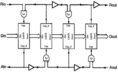
Using the 2 components discussed above, a 4 phase micropipeline can be constructed as shown in Fig. 4. Here, a 4 stage pipeline is shown with bubbled inputs to the Muller C element denoting inversion. Since propagation delay of the latch is greater than that of the Muller C elements, a delay has to be introduced in the path of the request signals in order to ensure proper synchronization between data and request signals. This delay is implemented using buffers having propagation delay comparable to that of the latches. This is because Muller C
Fig. 4 4 phase asynchronous pipeline
On initialization, all control signals are low and all latches are transparent. When valid data is present on Din, the request signal Rin is set which further makes the output of the Muller C high as both of its inputs become 1. This in turn sets the Cap signal thereby storing the data present in Din in the latch. Thereafter, Cap_d goes high to show that the latching is completed. The signal Cap_d is further propagated to the acknowledge signal Ain which is sent back to the sender denoting that the data has been received and the reset phase of the 4 phase protocol can start.
Moreover, Cap_d is also connected to the input of the Muller C of the second stage. This triggers the capture signal of the second stage high and the data output from the previous stage is latched into it. Again, the Cap_d signal goes high and will be forwarded to the Muller C elements of both the previous and the next stages. On one hand, it is sent to the positive input of the Muller C of the next stage thereby triggering data propagation in the third stage. On the other hand, it is sent to the negative input of Muller C element of the previous stage effectively giving 0 as the input to the Muller C. This matches with the Rin signal going low and hence marks the reset phase of the protocol. Now since both the inputs of the Muller C become 0, it gives 0 as the output which makes Ain low after resetting both Cap and Cap_d signals. This action completes the 4 phase protocol.
In this way, control and data signals are propagated through each stage of the pipeline strictly adhering to the 4 phase bundled data protocol. Finally, at the last stage, the request signal is sent out from the pipeline as Rout which can be used as the input control signal for the next module to send output data Dout from the pipeline to that module. Similarly, an acknowledge signal from the next module is input to the pipeline in the form of Aout after receiving the data. It is important to note that because of the reset phase of the 4 phase micropipeline, it is impossible to store data in the adjacent latches. Data is always held in alternate latches. Therefore, the number of latches used is twice the depth of the pipeline.
IV.VHDL MODELS
A. Asynchronous FIFO
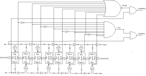
Using the concept of micropipelines explained in the previous section, an asynchronous FIFO has been created. This model of FIFO holds 15 bit wide data and has a depth of 4, which means it has 8 stages. A 15 bit data path may seem unconventional, but it is necessary as the control signals of SRAM are multiplexed with this data. Fig. 5 shows the interface signals of FIFO in which input ports are shown to the left and output ports to the right. Fig. 6 shows the block diagram giving its structural details.
Ports Rin, Ain, Rout and Aout perform the same functions as explained in the 4 phase micropipeline. The FIFO has added functionality through the ports Rst, Full, Empty, Overflow and Underflow. The FIFO is full when alternate latches hold data. Therefore, when capture signals to the alternate latches and inversion of the capture signals of the remaining latches give ‘1’ as the output when passed through a multiple AND gate, it means that the FIFO is full. Moreover, the FIFO is empty when all the latches are transparent. Therefore, if all capture signals give ‘1’ as the output when passed through a NOR gate, it implies that the FIFO is empty.
Fig. 5 Asynchronous FIFO: interface signals
The Rin signal going high if the FIFO is full will result in an overflow. Conversely, the Aout signal going high if the FIFO is empty will result in underflow. On making Rst high, the FIFO is reset. Hence, it will go back to its initial state with all latches transparent and all control signals low.
B. Asynchronous SRAM
The asynchronous SRAM presented in this paper has a capacity of 32 locations of 8 bits each. Fig. 7 shows its interface signals.
Fig. 7 Asynchronous SRAM: interface signals
The CE signal refers to Chip Enable and the SRAM function only when this signal is made high. When the request Rin goes high, the operation of the SRAM depends upon the W/R pin. If W/R is high, the 8 bit input data is sent through the Data_in (7:0) and stored in the addresses corresponding to the values given to the Address (4:0).
Whereas, if the Write/Read signal is low when the Req signal goes high, data will be read from SRAM and sent out through Data_out (7:0).
The Ack signal goes high in response to request for both read and write operations.
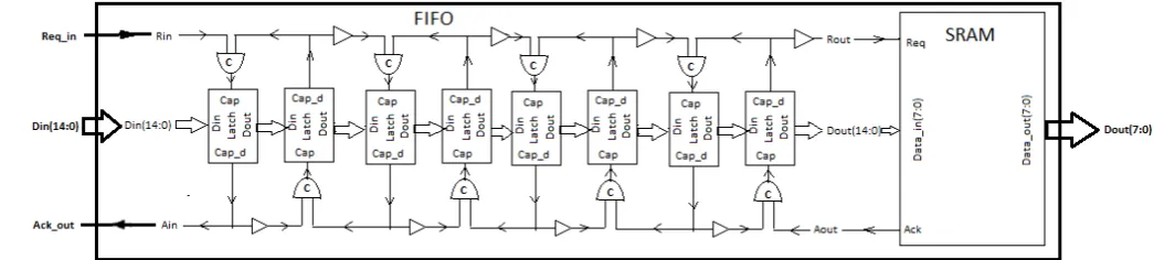
Fig. 8 FIFO-SRAM interfacing NGR schematic
Fig. 9 FIFO-SRAM interfacing block diagram
C. FIFO-SRAM Interfacing
Now the FIFO and SRAM are interfaced together to form a single unit which is assumed to be receiving signals from a controller. Fig. 8 shows the NGR schematic obtained during VHDL synthesis and depicts the ports of the entire system. Fig. 9 shows the block diagram of the data and handshaking signals. The double arrows show the data flow and single arrows show the control flow.
The control signals and addresses provided to the SRAM are multiplexed in the data input to the FIFO. In the 15 bit data, Din (14:0),
Din (14:7) is the actual 8 bit data.
Din (6:2) denotes the address values needed for storage in the SRAM
Din (1) specifies the W/R pin and Din (0) denotes the CE pin.
A step by step flow of data and control signals is outlined for this system.
Step 1: After system reset, all control signals are low and all latches empty.
Step 2: When valid 15 bit data is available, the Req_in is set which is connected to the input Rin of the FIFO making the latches in it ready for data capture. Rin propagates through each stage of the FIFO sequentially till it reaches the last stage. Step 3: The data is captured in the first latch of the
successive stage in accordance with setting up of the request signal of that particular stage, as explained in the 4 phase micropipeline description. Step 4: Simultaneously, an acknowledge Ain is sent back to the controller from the FIFO indicating that it has received the data. This Ain is connected to acknowledge Ack_out of the 2 module system.
Step 5: When data is available at the last stage of FIFO, request signal Rout is sent out from the FIFO and acts as the input request to the SRAM named Req.
Step 6: The SRAM receives the request and the 15 bit multiplexed data is input to it. If CE is high, and the W/R signal coming from the multiplexed data is high, the 8 bit data is written into the SRAM corresponding to the address values being input. If the W/R signal is low, the 8 bit data already stored in SRAM will be read and the data will be sent out from the SRAM in the form of Dout.
Step 7: The acknowledge Ack of the SRAM goes high after performing either a write or a read. This signal is sent back to the FIFO in the form of Aout which shows that the SRAM is ready for the next input from the FIFO.
V. SIMULATION RESULTS
The analysis involves calculating control delays and power consumed for the 15 x 4 FIFO interfaced with 32 x 8 SRAM using VHDL simulations.
A. Control Delays
Table II shows the control delays for the FIFO.
TABLE II
CONTROL DELAYS FOR FIFO
Path Delay(ns)
Rin ↑ to Rout ↑ 49.7
Rin ↑ to Ain ↑ 11.4
Rin ↓ to Ain ↓ 9.3
Aout ↑ to Ain ↓ 9.8
Aout ↑ to Rout ↓ 33.1 Aout ↓ to Rout ↑ 9.4 Total Cycle Time 122.7
It can be seen that the total cycle time for the FIFO comes out to be 122.7 ns. It should be noted that that above value shows the delay of the entire 8 stage FIFO. Delay of a single stage will be much less.
Total delay for the whole system from data going into Req_in to acknowledge coming out of Ack_out in Fig. 9, after travelling through both FIFO and SRAM is 58.1ns.
B. Power Analysis
The power analysis for the design is performed using Xpower Estimator which is a tool present in Xilinx ISE. Table III shows the power consumed by this design.
TABLE III POWER CONSUMED
Power Value (mW)
Dynamic 37 Quiescent 4 Total 41
An ambient temperature of 25° C is assumed for the analysis. As expected, the quiescent power is much lower than dynamic power which is the case for most circuits. The power consumed is less than comparable synchronous circuits.
VI.CONCLUSIONS
The results show the importance of using asynchronous systems in memory designs, specifically the FIFO-SRAM block which is essential for storing data. The use of a 4 phase micropipeline ensures fast and power efficient transfer of data and control signals from FIFO to SRAM which results in the development of high performance systems immune to clock skews.
The smooth functioning of this asynchronous FIFO-SRAM module reiterates the fact that we are steadily moving towards a future where asynchronous circuits will be ubiquitous.
REFERENCES
[1] I. E. Sutherland. Micropipelines. Communications of the ACM, 32(6):720–738, ISSN 0001-0782, 1989.
[2] A.V. Yakovlev, A.M. Koelmans, L. Lavagno,”High- Level Modeling and Design of Asynchronous Interface Logic”, IEEE Design and Test of computers, Spring 1995.
[3] Paul Day, J.Viv.Woods, "Investigation into Micropipeline Latch Design Styles" published in Very Large Scale Integration (VLSI) Systems, IEEE Transactions (Volume: 3, Issue: 2 ), ISSN :1063-8210, June 1995
[4] K.K. Yi, “The Design of a Self-Timed Low Power FIFO Using a Word-Slice Structure”, M.Phil Thesis, University of Manchester, September 1998.
[5] Chelceq T.; Nowick, S.M.; “Low-latency asynchronous FIFO’s using token rings”; Advanced Research in Asynchronous Circuits and Systems, 2000. (ASnVC 2000) Proceedings. Sixth International Symposium, 2-6 April 2000 Pages: 210 - 220
[6] J. Sparso, S. Furber, “Principles of Asynchronous Circuit Design: A Systems Perspective”. European Low-Power Initiative for Electronic System Design, Kluwer Academic Publishers, ISBN: 0-7923-7613-7, Jan 2002.
[7] Xin Wang, Tapani Ahonen, Jari Nurmi , “A synthesizable RTL design of asynchronous FIFO”. System-On-chip Proceedings, November 2004
[8] Chammika Mannakkara, “Asynchronous Pipeline Controller Based on Early Acknowledgement Protocol”, September 2010
![Fig 1 shows the waveforms using this protocol [8].](https://thumb-us.123doks.com/thumbv2/123dok_us/7828898.1297282/1.595.309.556.310.429/fig-shows-waveforms-using-protocol.webp)