Plasma-assisted formation of low defect density SiC–SiO
2interfaces
A. Go¨lz
Institut fur Halbleitnertechnik, RWTH-Aachen, Aachen D-52074, Germany
G. Lucovsky,a)K. Koh, D. Wolfe, and H. Niimi
Departments of Physics, Materials Science and Engineering and Electrical and Computer Engineering, and Chemistry, North Carolina State University, Raleigh, North Carolina 27695-8202
H. Kurz
Institut fur Halbleitnertechnik, RWTH-Aachen, Aachen D-52074, Germany
~Received 24 February 1997; accepted 22 April 1997!
The initial stages of SiC–SiO2 interface formation by low temperature ~300 °C! remote plasma assisted oxidation~RPAO!on flat and vicinal 6H SiC~0001!wafers with Si faces have been studied by on-line Auger electron spectroscopy ~AES!. Changes in AES spectral features associated with Si–C and Si–O bonds are readily evident as oxidation progresses; however, there are no detectable AES features that can be attributed to C–O bonds. Initial oxidation rates as determined from AES data are greater for vicinal wafers than for flat wafers paralleling results for RPAO oxidation of Si. Devices fabricated on vicinal SiC wafers require an 1150 °C anneal in an H2containing ambient to reduce defect densities from the 1013to 1011cm22range, consistent with termination of C atom step edge dangling bonds by H atoms. Devices prepared by thermal oxidation also require a 1150 °C anneal in H2 even though silicon oxycarbide regions with C–O bonds are formed in a transition region at the SiC–SiO2 interfaces. © 1997 American Vacuum Society.@S0734-211X~97!07304-6#
I. INTRODUCTION
There is considerable interest in SiC for high temperature device applications, including power transistors. To fabricate these devices, it will be necessary to gain an increased un-derstanding of the chemical bonding at the SiC–SiO2 inter-face, and in particular to develop processing that minimize interfacial defects and transition regions, and maximize de-vice reliability as manifested in reductions in the rate of in-terfacial and bulk defect generation during operation. It has been established that the oxide that forms on SiC during high temperature oxidation in O2 ambients is SiO2, and that this oxidation process can yield SiC–SiO2 interfaces and gate dielectrics with sufficiently low defect densities for field ef-fect transistor~FET!operation.1However, channel mobilities at room temperature ~in depletion mode FETs! are signifi-cantly lower than expected from bulk SiC properties and much research has been focused on explaining these differ-ences and improving channel mobilities.2 Since SiO2 is the dominant solid state oxidation product, oxidation products involving carbon atoms must include gaseous molecules such as CO; as oxide growth progresses these must be trans-ported from the buried growth interface through the oxide and out of the film. However, this does not preclude the formation of additional interfacial carbon atom bonding ar-rangements such as Si–C and C–O as have been reported in silicon oxycarbide transition regions.3 The molar volume mismatch between SiC and SiO2 is greater than the corre-sponding mismatch between Si and SiO2, so that intrinsic levels of strain at SiC–SiO2 interfaces are anticipated to be at least as high as the values of approximately 5
3109 dynes/cm2 reported in Si–SiO2. 4
This article deals
with an alternative low temperature method for semiconductor-dielectric interface formation that has been successfully applied to crystalline Si device technology.5,6 As applied to Si, this approach provides independent control of Si–SiO2 interface formation and dielectric film grown. The Si–SiO2 interface and a superficially thin oxide layer ~;0.5 nm!are formed by a low temperature~300 °C!remote plasma-assisted oxidation ~RPAO!process, and the remain-der of the oxide layer is deposited by a low temperature ~300 °C!remote plasma enhanced chemical vapor deposition ~RPECVD! process. Device quality interfaces are obtained by subjecting the plasma processed Si–SiO2 heterostructure to a post-deposition rapid thermal anneal~RTA!, e.g., for 30 s at 900 °C. The 900 °C anneal promotes both chemical and structural interface relaxations, including a minimization of interfacial sub-oxide bonding arrangements in transition re-gions between the Si crystal and the stoichiometric bulk oxide.7 A similar plasma-assisted process has recently been applied to SiC, and has yielded SiC–SiO2 interfaces with defect state densities comparable to what has been achieved on SiC by conventional high temperature thermal oxidation.8 The potential advantages of this two step approach to SiC– SiO2 interface formation are: ~i! it reduces the requirement for transporting gaseous reaction products such as CO mol-ecules away from the interface as the oxide grows; and~ii!it can also reduce strain induced interface defect generation, since only a small fraction of the total oxide layer thickness is generated by consumption of the SiC substrate. The focal point of this article is a study of SiC–SiO2 interface forma-tion by RPAO using on-line Auger electron spectroscopy ~AES!to monitor interface bonding chemistry and the initial oxide growth rate.
to summarize the results of device studies on vicinal Si and SiC wafers using the plasma-assisted processing steps iden-tified above. Studies by Bjorkman et al.9 demonstrated that densities of mid-gap defect states (Dit) as low as 1
31010cm22 eV21 could be obtained on Si~111!surfaces by using conventional thermal oxidation, metal electrodes and 400 °C post metal anneals in an H2 containing ambient. Pre-vious studies had always shown higher values for Si~111!as compared to the Si~100!surfaces used in the integrated cir-cuit wafers~see Reference 9!. Studies performed by Yasuda
et al. on p-type Si~111!vicinal up to 5° in the 112¯ direction showed that the density of mid-gap states (Dit) increased by relatively small amounts from ;131010cm22 eV21 to about 631010 cm22 eV21 as the vicinal angle increased to about 5°.10 The studies of Yasuda et al. were on Si–SiO2 structures prepared by the same two-step RPAO-RPECVD 300 °C process that has been described above, and is dis-cussed in detail in Ref. 5. Al electrodes were employed and a 400 °C postmetallization anneal ~PMA! in a H2 containing ambient was used. The magnitudes of the incremental in-creases in Dit with increasing vicinal angle indicated that only a relatively small fraction of the dangling bond states at the step edges contributed to increases in Ditwith increasing step edge density due to increasing vicinal angle.
At the present state of the art, the highest quality SiC crystals for devices are epitaxial layers formed on Si atom terminated 6H SiC vicinal approximately 3.5° in the 112¯0 direction. Using RPAO-RPECVD, the results of device stud-ies using vicinal 6H p-type SiC as reported by Go¨lz et al.7 are markedly different than the results reported for vicinal Si. Metal-oxide-semiconductor~MOS!capacitors were prepared the essentially the same two-step RPAO-RPECVD process as used by Yasuda et al.5for Si. However, following a con-ventional PMA in an H2containing ambient, Ditvalues were in excess of 1013cm22 eV21, even when an 1150 °C fur-nace anneal in Ar was interposed between the oxide film deposition and the metallization steps. However if the high temperature anneal was performed in an H2 containing am-bient then Dit values after the conventional 400 °C PMA were reduced significantly into the 1011cm22 eV21 range.8 This large difference in defect densities is approximately equal to the number of carbon atom dangling bonds at the step edges suggesting that these dangling bonds were not H-terminated after a conventional 400 °C PMA, but instead required the higher temperature exposure to H for termina-tion. It is important to note that interfaces prepared on the same type of vicinal SiC surfaces by conventional high tem-perature thermal oxidation processes also required a high temperature anneal in an H2containing ambient to yield val-ues of Ditin the 1011cm22 eV21 range.10Step edge carbon atom dangling bonds on vicinal Si wafers can either termi-nated by oxygen atoms that connect into the SiO2 dielectric, or by hydrogen atoms. The annealing results in Refs. 8 and 10 are consistent with hydrogen atom termination of step edge carbon atom dangling bonds~see Section II for atomic structure at the step edges!; i.e., dangling bond elimination
would be accomplished by atomic hydrogen generated dur-ing the 1150 °C anneal.
To study interfacial bonding arrangements between SiC and SiO2, on-line AES has been used to monitor the initial stages of SiC–SiO2 interface formation. This same approach has been used to study the initial stages of interface forma-tion on Si by both RPAO and rapid thermal oxidaforma-tion~RTO!, and using both O2 and N2O oxygen atoms sources gases.
7
This article extends this approach to SiC and focuses on the initial stages of the RPAO process as applied to both flat or vicinal SiC surfaces using O2 source gases. Preliminary re-sults are also presented for RPAO using N2O as the oxygen atom source gas. Section II discusses briefly the local bond-ing arrangements at the step edges of the vicinal 6H SiC wafers. Section III presents results of AES studies of SiC RPAO, and includes comparisons between the RPAO of SiC and Si. Detailed results are presented for RPAO using O2, and preliminary results for RPAO using N2O. Section IV summarizes the major results of this study as they apply to ~i!the results of the on-line AES studies, and~ii!the passi-vation of step edge dangling bonds as revealed by changes reductions in Ditlevels as determined from electrical mea-surements.
II. LOCAL BONDING AT STEP EDGES
per double layer Si–C component, and the second set of steps are an ACB sequence with two carbon atom dangling bonds per double layer Si–C component. The average num-ber of dangling bonds per step in 6H SiC~0001!is 1.5 dan-gling bonds per step edge atom, whereas in Si~111!off cut in the 112 direction it is only 1 dangling bond per step atom. The spacing between single steps on Si~111!off cut in the 112 direction is ;5 nm for a 3.5° off cut angle, so that the ratio of step edge to terrace dangling bonds is approximately 0.06. For a 3.5 off cut angle on SiC, the dangling bond ratio is higher by a factor of 1.5 due to the different step edge terminations of the ABC and ACB sequences. If the 6H SiC surface has two atom steps, as is likely for the wafers used in this study, the dangling bond considerations are the same. Starting with the same ABC sequence as in Fig. 1, the first three 2 atom steps are terminated by C atoms with one dan-gling, and the second three 2 atom steps by C atoms with two dangling bonds. This means that the number of dangling bonds per step on the average is still 1.5 times greater than for off cut Si wafers.
III. EXPERIMENTAL RESULTS
The samples used in this study were p-type 6H SiC pur-chased from Cree Corporation with Si faces. Similar to polar faces on III–V compounds, the polar faces on SiC are either Si or C faces. Note further that this particular designation is used independent of any surface contamination. One of the wafers was oriented on a principal axis, the~0001!direction, and the other was a vicinal wafer off cut at approximately 3.5° in the 112¯0 direction. The surface of the on-axis sample was prepared from and bulk ingot, and the surface of the off-axis sample used in these studies was from an epitaxially grown film. The surfaces of the wafers were cleaned follow-ing a procedure suggested by Cree Research, Inc.11 The ex
situ cleaning consisted of ~i! sequential rinses in tri-chloro-ethane~TCE!, acetone and methanol, followed by~ii!a con-ventional two bath RCA clean. The sacrificial oxide formed in the second step of the RCA clean was removed by rinse in dilute HF. Samples were then loaded into a multichamber system, which provides a separate ultrahigh vacuum~UHV! compatible chambers for RPAO and AES. The experimental procedure was to alternate AES measurements with RPAO processing. A similar approach has been applied to RPAO of Si, and through analysis of the AES data, two kinds of infor-mation were obtained: ~i! the chemical bonding at the Si– SiO2 interface, and ~ii!the oxide thickness as a function of oxidation time.12
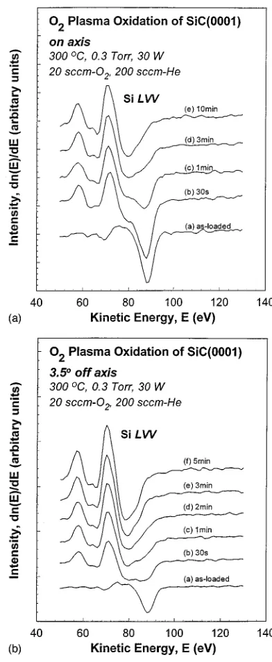
Figures 2~a!and 2~b!, respectively give differential AES spectra for flat and vicinal SiC obtained by RPAO using an O2 source gas. The experimental processing conditions are: ~i! a substrate temperature of 300 °C,
~ii! a process pressure of 300 mTorr,
~iii! a plasma power to the He/O2 mixture of 30 W, and ~iv! flow rates 200 standard cubic centimeters per minute
~sccm!of He, and 20 sccm and O2.
The as-loaded samples show surface contamination by
oxy-gen and nitrooxy-gen that was not removed by the ex situ clean-ing process. Since the levels of surface contamination were sub-monolayer, no in situ cleaning was attempted. This was in part due to the limited temperature capabilities of the plasma-processing chamber; the substrate heater in this chamber cannot heat a wafer to a temperature greater than about 500 °C. Never-the-less, the nitrogen contamination problem must be overcome before detailed studies of inter-face bonding using an N2O source gas can be definitive with respect to any preferential nitrogen atom incorporation at the SiC–SiO2 interface. It should be further noted that the SiC samples used in this study were n-type with a N atom doping level of ;1.431018cm23, so that the N contamination FIG. 2. Derivative mode AES spectra for~a!flat and~b!vicinal SiC obtained by RPAO at 300 °C using O2as the oxygen atom source gas.
may have its origin in the doping of the SiC wafers; how-ever, it cannot be attributed simply to the doping because the area density of dopant atoms in a 2 nm thickness~;2 elec-tron escape depths! is;331011cm22, which is consider-ably less than the minimum AES detection limit of ;1013 cm22. In spite of the sub-monolayer surface N con-centration, information relative to oxidation rates could be obtained using the N2O source gas. In the case of Si, as-loaded samples generally showed small levels of oxygen contamination, but never showed any nitrogen signal, so that more detailed interface bonding studies could be performed with both O2and N2O source gases.12Prior to oxidation, the flat and vicinal SiC wafers displayed essentially the same (63%) Si/C surface ratios so that changes in these ratios could be correlated with the effects of the oxidation pro-cesses. As the oxidation time for the SiC wafers is increased, there are four changes evident in the SiC spectra in Figs. 2~a! and 2~b!:
~i! the line shapes and multiplicity of features within the SiLVVgroup changed,
~ii! the CKVVsignal strength decreased, ~iii! the NKLL signal strength decreased, and ~iv! the OKLL signal strength increased.
These spectral changes are consistent with the growth of an SiO2 film on the SiC substrate.
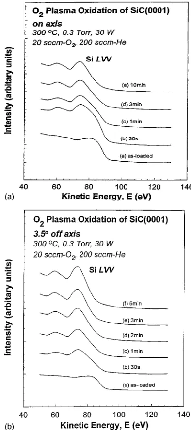
Figures 3~a!and 3~b!, and 4~a! and 4~b!display, respec-tively, changes in ~a! the SiLVV and ~b! the CKVV ~AES! features as a function of the oxidation time for flat ~Fig. 3! and vicinal~Fig. 4!surfaces. Consider first the SiLVVfeatures in Figs. 3~a!and 4~a!. The feature at;88 eV is associated with Si–C bonds, in particular with a Si atom that is bonded to four C atoms. As the oxidation proceeds this feature de-creases in strength as the Si–O feature at;76 eV increases. These changes in relative intensity are due to increase of the oxide thickness with time and are consistent with the relative values of the electron escape depth,;0.6 nm, and the oxide thickness. There is also a shift of the Si–C feature to lower energy as the oxidation proceeds; this is more easily seen in the spectra for the off-axis sample. Figures 5~a! and 5~b! display the integrated SiLVVspectra. It is evident from Figs. 3~a! and 5~a! that as the intensity of the Si–C feature de-creases, the position of this spectral feature moves to lower energy. In particular in Fig. 3~a!, the Si–C feature is evident as a distinct spectral peak at;88 eV prior to oxidation, after the oxidation has progressed for 3 min it has shifted to lower energy and appears as shoulder at ;84 eV on the 76 eV peak. In contrast, the C–Si feature in the CKVVspectrum in Fig. 4~a!simply decreases in strength as the oxidation pro-cess proceeds. The absence of any significant spectral change in this region of the AES spectrum is indicative of the fact that C–O bonds are not formed during the RPAO process. The development of interfacial C–O bonds would produce a satellite peak at lower energy, which would increase in rela-tive strength to the C–Si feature as the oxide growth pro-ceeds and the AES signal becomes more sensitive to the SiC interface than the bulk.
The oxide thickness can be obtained to 65% from the relative intensity changes in the CKVVfeature using the char-acteristic escape depth of 0.96 nm for 275 eV electrons. A similar approach has been applied for the determination of the oxide thickness for the RPAO process on Si, and has been validated by a direct measurement of oxide thickness by cross-sectional high resolution transmission electron mi-croscopy.
Figures 6~a!and 6~b!shows log-log plots, respectively of the oxide thickness versus the oxidation time for the RPAO of ~a!Si and~b!SiC for the O2source gas. In each instance the data can be fit by a power law dependence of the form, tox5Atb, where tox is the oxide thickness in nm, t is the oxidation time in minutes, and A and b are fit FIG. 3. Changes in the SiLVVAES features as a function of the oxidation time for~a!flat and~b!vicinal SiC surfaces for O2RPAO.
parameters.12,13The initial oxidation rates are about one and one-half times faster for the vicinal than for the flat wafers, and the initial oxidation rates are faster for Si than for SiC. However, the power law exponents for the SiC oxidations for both flat and vicinal surfaces are greater than the corre-sponding exponential factor for Si; however, all of the these power law exponents are less than 1. The relative differences in the power law factors means that at long times of about 10 min or more the thicknesses of the oxides formed on both Si and SiC are comparable for both the flat and vicinal wafers. Figure 7 illustrates this by showing a comparison of oxide thickness versus oxidation time for flat Si and SiC; a similar situation also prevails for the oxidation of the off-axis wa-fers.
Finally for the RPAO of Si using the same relative flow rates of N2O and O2, the oxide growth rate was slower by a factor of 2 using the N2O source gas.12 Comparisons of RPAO rates have also been made for SiC for plasma excited O2and N2O source gases. For the same relative flow rates of these two source gases, the situation is reversed with respect to Si, i.e., the oxidation rate of SiC is greater using the N2O source gas. This increased growth rate using plasma excited species from the N2O discharge is illustrated in Fig. 8 for the RPAO of flat SiC wafers.
IV. DISCUSSION AND SUMMARY
A. AES results
The analysis of the AES spectra for the flat and vicinal SiC surface RPAO processes using the O2 source gas indi-cates:
FIG. 4. Changes in the CKVVAES features as a function of the oxidation time for~a!flat and~b!vicinal SiC surfaces for O2RPAO.
FIG. 5. Integral, n~E!, SiLVVAES spectra as a function of the O2 RPAO oxidation time for~a!flat and~b!vicinal SiC surfaces.
~i! the solid state oxidation product is SiO2; ~ii! there are no interfacial C-O bonds; and
~iii! oxidation proceeds initially more rapidly on vicinal surfaces than on flat surfaces, paralleling what has been found for Si.
The primary solid state oxidation product for thermal oxida-tion of SiC is also SiO2; however, there have been reports of the observation of C–O at or near the SiC–SiO2 interface.3 This means that there are significant differences in the oxide formation chemistries by low temperature plasma assisted and high temperature thermal oxidation processes. For ex-ample, in the plasma assisted processes the oxidation species are typically long-lived molecular metastables such as O2*or positive molecular ions such as O21, whereas in the thermal
oxidation process the oxidation species are typically O at-oms. Since the thermal and plasma oxidation processes are qualitatively different with respect to the formation of C–O bonds, then the differences between the two types oxidation processes could be expected to require different post-oxidation and post-deposition procedures for forming low defect density SiC–SiO2 interfaces. However, this is not the case, as is discussed in Sec. IV B of the article. Before
dis-FIG. 6. Log-log plots of the oxide thickness versus the oxidation time for the O2RPAO of flat and vicinal~a!Si and~b!SiC. The data are fit to a power law dependence, tox5atb.
FIG. 7. Log-log plots comparing oxide thickness versus the oxidation time for the O2RPAO of flat Si and SiC. The data are fit to a power law depen-dence, tox5atb.
FIG. 8. Log-log plots comparing the oxide thickness versus the oxidation time for the RPAO of flat SiC using O2and N2O as the oxygen atom source cases. The data are fit to a power law dependence, tox5at
b .
cussing this aspect of the experimental results, additional as-pects of the power laws fits are discussed below.
The power laws fits to RPAO data show that the oxidation process proceeds very rapidly initially and then slows down considerably with increasing oxidation time. This means chemical reaction rates between excited oxygen species and Si- and Si- and C atom dangling bonds on Si and SiC, re-spectively, are decreased after Si–O bonds and a superficial layer of SiO2 are formed at the onset of RPAO.
14
For the case of RPAO of Si the oxidation rate for flat surfaces is faster using O2 than N2O for the same relative flow rates of He and O2 or N2O. For the RPAO of SiC the situation is reversed for flat surfaces and the oxidation rate is faster using N2O. Studies are currently underway to address this difference. A model has been proposed for RPAO of Si that explains the differences in the oxidation rates using O2 or N2O source gases.15This model was developed primarily to explain the retention of nitrogen atoms at the Si–SiO2 interface during oxide growth using the N2O source gas. The surface contamination of SiC by nitrogen makes it impos-sible to determine whether there is nitrogen retention at the SiC–SiO2interface during oxide growth in N2O. This issue is presently under study, and will require the development of procedures for ex situ surface preparation that remove re-sidual nitrogen atom contamination from the SiC surface.
B. Electrical properties of SiC–SiO2 interfaces
This section summarizes results of recent electrical mea-surements made on MOS capacitors, in particular it com-pares values of Dit as extracted from capacitance-voltage measurements on SiC interfaces prepared on p-type sub-strates. The experimental studies of Stein von Kaminski
et al.11 have demonstrated mid-gap Dit values in the low 1011 cm22 eV1 range for interfaces prepared by high tem-perature thermal oxidation. These device structures used metal electrodes. The attainment of low defect densities re-quired two annealing steps:
~i! a post-oxidation an Ar/H2 mixture at 1150 °C, and ~ii! a conventional PMA in an H2 containing ambient at
400 °C after metallization.
When annealing procedures that did not include H2 in the 1150 °C anneal were applied to the RPAO formed interfaces, the Dit values were significantly higher, in the 1013 cm22 eV21range.7However as shown in Ref. 8, these Dit values were significantly reduced for the RPAO inter-faces following a high temperature ~1150 °C! anneal in an Ar/H2 mixture. It is interesting to note that the difference in Dit values between RPAO devices subjected to the Ar and Ar/H2 anneals is very nearly equal to the density of carbon atom dangling bonds at the step edges. This suggests the possibility that carbon atom dangling bonds are not termi-nated by during the oxidation or oxide deposition steps, or during the conventional PMA.
Consider first the RPAO interfaces. Since our studies show no C–O bonding in interfacial regions for either the flat or vicinal wafers, it is suggested that the step edge carbon
atom dangling bonds may remain unterminated after the oxi-dation process. The high defect density after the conven-tional 400 °C PMA in a hydrogen containing ambient further suggests that the step edge carbon atom dangling bonds are not hydrogen terminated by this process. If this is the case then hydrogen atom production during the 1150 °C anneal in Ar/H2 is sufficiently high to produce C–H bonding at the step edges. Since thermal oxidation processes show evidence for C–O bonding in interfacial transition regions3 and the RPAO process does not, this suggests that there might be differences related to the way step carbon atom dangling bonds are terminated, either during thermal and plasma oxi-dations, or in post-oxidation annealing. However, this ap-pears not to be the case, since interfaces produced by high temperature thermal oxidation also require a high tempera-ture anneal in an H2 containing ambient. This means that even though C–O bonds can be found in silicon oxycarbide transition regions after high temperature thermal oxidation3 they may not be formed in sufficient numbers at carbon atom step edges to neutralize dangling bond defects. Alternatively, the local bonding environment of carbon atoms in interfacial regions and at the Si–C step edges is different and may be a contributing factor to oxygen atom termination.
Finally, it is also interesting to note that fabrication of low Ditinterfaces on n-type SiC by RPAO and thermal oxidation does not require a high temperature anneal in an H2 contain-ing ambient.7 There are two possible explanations for not requiring such an anneal for the RPAO formed interfaces: ~i! the active interfacial defects are in the bottom half of
the SiC band gap and hence are more active in
p-type material, or
~ii! the formation of C–O bonds at an SiC interface is Fermi level dependent favoring C–O bond formation in n-type material.
The wafers that we studied were nitrogen doped n-type wa-fers, and there was no evidence of interfacial C–O bond formation. However, the concentration of step edge C atom danglings bonds that are available for termination by C–O bonding is below the AES detection limit. 6H SiC flat and vicinal SiC wafers with C faces have been ordered from Cree Research, Inc., upon their receipt, an AES study of the initial stages of PRAO will be initiated. It is clear that these ques-tions identified with respect to electrical results on SiC de-vices need additional experimental and theoretical studies before they can be satisfactorily resolved. In particular, elec-tron spin resonance experiments that can readily distinguish between Si and C atom dangling bonds may be helpful in resolving the issues discussed in the last two paragraphs.
ACKNOWLEDGMENTS
This research has been supported by the the National Sci-ence Foundation, Office of Naval Research, and Air Force Office of Scientific Research ~Multi-University Research In-tiative!.
1L. A. Lipkin and J. W. Palmour, J. Electron. Mater. 25, 909~1996!. 2
T. Ouisse, Philos. Mag. B 73, 325~1996!.
3B. Hornetz, H.-J. Michel, and J. Halbritter, J. Mater. Res. 9, 3088
~1994!.
4J. T. Fitch, E. Kobeda, G. Lucovsky, and E. A. Irene, J. Vac. Sci.
Tech-nol. B 7, 153~1989!.
5T. Yasuda, Y. Ma, S. Habermehl, and G. Lucovsky, Appl. Phys. Lett. 60, 434~1992!.
6
G. Lucovsky, Yi Ma, S. V. Hattangady, D. R. Lee, Z. Lu, V. Misra, J. J. Wortman, and J. L. Whitten, Jpn. J. Appl. Phys. 1 33, 7061~1994!. 7G. Lucovsky, A. Banerjee, B. Hinds, B. Claflin, K. Koh, and H. Yang, J.
Vac. Sci. Technol. B, these proceedings. 8
A. Go¨lz, R. Janssen, E. Stein von Kamienski, and H. Kurz, in The Physics
and Chemistry of SiO2and the Si–SiO2Interface, edited by H. Z.
Mas-soud, E. H. Poindexter, and C. R. Helms~Electrochemical Society, Pen-nington, NJ, 1996!, p. 753.
9C. H. Bjorkman, C. E. Shearon, Jr., Y. Ma, T. Yasuda, G. Lucovsky, U. Emmerichs, C. Meyer, K. Leo, and H. Kurz, J. Vac. Sci. Technol. B 11, 964~1993!.
10
T. Yasuda, D. R. Lee, C. H. Bjorkman, Y. Ma, U. Emmerichs, C. Meyer, K. Leo, and H. Kurz, Mater. Res. Soc. Symp. Proc. 315, 375~1993!. 11E. Stein von Kaminski et al., Microelectron. Eng. 28, 201~1995!. 12G. Lucovsky, H. Niimi, K. Koh, D. R Lee, and Z. Jing, in Ref. 8, p. 441. 13D. R. Wolters and A. T. A. Zegers-van Duynhoven, J. Appl. Phys. 65,
5126~1989!.
14P. Thanikasalam, T. K. Whidden, and D. K. Ferry, J. Vac. Sci. Technol. B 14, 2840~1996!.
15K. Koh, H. Niimi, and G. Lucovsky, Mater. Res. Soc. Symp. Proc.~in press!.