Logical Supportive Interface to Hardware
Description for Analog Design Interface
R.Prakash Rao1 , Dr.B.K.Madhavi2
1
St.Peter’s Engineering College,Near Forest Academy, Dulapally,Hyderabad.
2Geetanjali College of Engineering and Technology, Cheryala, Hyderabad.
Abstract-- The integration of the transistor levels in one single platform
is rapidly increasing. With the increase in the integration the concept of system on chip (SoC) is evolving. Researchers are in focus to integrate multiple units into a single platform to achieve the objective of reliable and effective VLSI chips. For the integration of such system the modeling of all the embedding devices are to be coded in one single platform. The hardware description language (HDL) is one such prominently used environment. HDL is used as a definition platform for digital systems, but for the SoC modeling where both analog and digital systems are required the design methodology is not supported. To overcome this limitation in this paper we present a designing approach for designing and modeling of analog operation on digital environment.
Keywords-- Analog modeling, SoC designing, HDL modeling, Digital
Designing
I.INTRODUCTION
The use of digital signal processing has become widespread, and it provides enormous advantage over analog voice signals. One of the most important applications of digital signal Processing is on long distance telephone communications. Digital signal can be passed through an almost unlimited number of repeaters with negligible degradation. Analog signals, on other hand, suffer a large amount of degradation each time they are passed through a repeater. This makes digital communication to be more advisable than analog communication for long distance communication. Digital signal can easily be switched using multiplexing, and a large number of digital signals can be combined on a single link by time division multiplexing. Digital signal has several other advantages. For example, in military systems it can easily be encrypted for secure voice transmission. It is much easier to scramble the bits of a digital signal than to scramble an analog signal. Another advantage in some links, where the transmission path is poor, is that powerful error correction codes can be used to reduce the error rate as much as required, whereas with analog transmission, distortions and noise in the transmission path cannot be removed easily. Digital signal may also be stored and retrieved without loss of quality. High-quality digital signal requires a high bit rate that, if transmitted, results in significantly wider bandwidth over the analog signal form, which it originated. Sophisticated digital signal processing techniques are employed to reduce the data rate. It is well known from Fourier theory that a signal can be expressed as the sum of a, possibly infinite, series of sines and cosines. This sum is also referred to as a Fourier expansion. The big disadvantage of a Fourier expansion however is that it has only frequency resolution and no time resolution.
II.DIGITAL MODELING
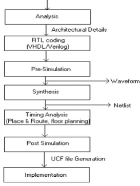
Figure 1 shows a typical process for the design of a digital system. An initial design idea goes through several transformations before its hardware implementation is obtained. At each step of transformation, the designer checks the result of last transformation adds more information to it & passes it through to the next step of transformation. Initially, a hardware designer starts with a design idea. A more complete definition of the intended hardware must be developed from the initial design idea. Therefore, it is necessary for the designer to generate a behavioral definition of the system under design. The product of this design stage may be a flow chart, a flow graph, or pseudo code. The designer specifies the overall functionality and an i/p to output mapping without giving architectural or hardware details of the system under design.
Fig.1 VLSI Design Flow Diagram
The next phase in the design process is the design of the system data path. In this phase, the designer specifies the register and logic units necessary for implementation of the system. These components may be bidirectional or unidirectional busses. Based on the intended behavior of the system, the procedure for controlling the movement of data between register and logic units through busses is then developed.
A. Design Automation
From designer point of view, the design phase is complete when an idea is transformed into architecture or a data path description. The rest is routine work and involves tasks that a machine can do much faster than a talented engineer. The same can be said about the verification process; that is. a machine can be programmed to verify functionality or timing of a designed circuit much easier than any human can. Activities such as transforming one form of a design into another, verifying a design stage output, or generating test data can be done at least in part by computers. This process is referred to as design automation (DA).
Design automation tools can help the designer with design entry, hardware generation, test sequence generation, documentation, verification, and design management. Such tools perform their specific tasks on the output of each of the design stages of Figure 1.
III.SYSTEM DESIGN
For many signals, the low-frequency content is most important part. It gives the signal its identity. The high-frequency content, on the other hand, provides the add on properties to it. Eg. in a human voice if high-frequency components are removed, the voice sounds different, but, if enough of the low-frequency components are removed the complete signal may be lost. In wavelet analysis, approximations and details are the parameters to be obtained. The approximations are the high-scale, low frequency components of the signal. The details are the low-scale, high frequency components. The original signal, S, passes through two complementary filters and emerges as two signals. If the operation is performed on the real digital signal, twice the number of data samples is obtained. Eg. If an original signal S consists of 1000 samples of data. Then the resulting signals will each have 1000 samples, for a total of 2000. These signals A and D are interesting, but 2000 values were obtained instead of the 1000. Performing carefully at the computation, only one point out of two in each of the two 2000-length samples is sufficient to get the complete information. This is the notion of down sampling. This result in two sequences called cA and cD.
The decomposition process can be iterated, with successive approximations being decomposed in turn, so that one signal is broken down into many lower resolution components. This is called the wavelet decomposition tree. The wavelet decomposition tree can be obtained by the implementation of a chain of High pass and low pass filter banks as given below.
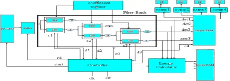
Fig.2 Architectural block diagram for Implemented decomposer module
A.Operational Description
Fig.2 shows the architectural block diagram for Implemented decomposer module. The input sampled signals having 16 bit each are applied in parallel to sub band mapping module. After the 12th sample passes to FIFO input unit, four sampled signals are passed down to input buffer as a packet. Input FIFO stores 12 samples of sampled signal each in which samples are represented in 16 bit floating point notation. After every 12 samples stored in FIFO first 4 samples are passed from FIFO to the input buffer and then fed to the sub-band filter bank block through the wavelet decomposition. This sub-band carries out filter decomposition of the given input signal of the length 4 samples, considering a bank of Low Pass Filter and High Pass Filter. The filter takes 4 filter coefficients for LPF and HPF obtained from db4 wavelet with the length of 4, which were derived from Matlab. Convolution operation takes on input signal with filter coefficient to obtain detailed and approximate coefficients after down sampling by 2. Each sub-band carries 3 points for passing of every 4 samples. A total of 9 points are obtained for 12 samples passed in each sub-band thus this sub-band unit mapping carries out wavelet decomposition using wavelet filter bank in to 4 sub-bands each sub-band with 9 points. Obtained sub-band samples are stored in sample RAM & its corresponding energies are calculated by the energy calculator module and stored in energy RAM. Scale factor for the sub-band is the sample with maximum amplitude in the sub-band obtained from the comparator module where the comparator module compares all the sample of each subband and find the maximum of it. Fig. 3 shows the block diagram for Implemented reconstructor module.
Fig. 3 Block diagram for Implemented reconstructor module
IV.HDL MODELING
The filter logics are realized using MAC (multiply and accumulate) operation where a recursive addition, shifting and multiplication operation is performed to evaluate the output coefficients. The recursive operation logic is as shown below Fig.4
Fig. 4 Realization of recursive MAC operation
Multiplier Adder
Shifter
Input coefficients
Filter coefficients
Before passing the data to filter bank the fifo logic realized, stores the data in asynchronous mode of operation, operating on the control signals generated by the controller unit. On a read signal the off-centered data is passed to the buffer logic. The fifo logic realized as shown below Fig.5
Fig.5 Realization of 16 x 16 fifo logic for coefficient interface
The obtained detail coefficients are down sampled by a factor of two to reduce the number of computation intern resulting in faster operation. To realize the decimator operation comparator logic with a feedback memory element is designed as shown below Fig.6
Fig.6 Architecture for decimation by 2 logic
The proposed system is realized using VHDL language for it’s functional definition. The HDL modeling is carried out in top-down approach with user defined package support for floating point operation and structural modeling for recursive implementation of the filter bank logic. For the realization a package is defined with user defined record data type as type real_single is
record sign : std_logic;
exp: std_logic_vector(3 downto 0); mantissa: std_logic_vector(10 downto 0); end record;
The floating notation is implemented using 16 bit IEEE-754 standards as presented below.
Sign. (1) Exp. (4) Mantissa (11)
The floating-point addition, multiplication and shifting operation are implemented as procedures in the user defined package and are repeatedly called in the implementation for recursive operation. The procedures are defined as;
procedure shifftl (arg1: std_logic_vector;arg2: integer;arg3 :out std_logic_vector);
procedure shifftr (a:in std_logic_vector; b:in integer;result: out std_logic_vector);
procedure addfp (op1,op2: in real_single;op3: out real_single) ;
procedure fpmult (op1,op2: in real_single;op3: out real_single) ;
for performing the convolution operation, filter coefficients are defined as constant in this package and are called by name in filter implementation.
constant lpcof0: real_single:=('1',"0100","00001001000"); constant lpcof1: real_single:=('0',"0100","11001010111"); constant lpcof2:real_single:=('0',"0110","10101100010"); constant lpcof3:real_single:= ('0',"0101","11101110100"); constant hpcof0: real_single:= ('1',"0101","11101110100"); constant hpcof1:real_single:=('0',"0110","10101100010"); constant hpcof2:real_single:=('1',"0100","11001010111"); constant hpcof3:real_single:=('1',"0100","00001001000");
Using the above definitions the filters are designed for high pass and low pass operation. The recursive implementation is defined as;
for k in 1 downto 0 loop old(k):=shift(k);
fpmult(old(k)(0),hpf(k+1),pro(k)(0)); proper(j,k):=pro(k)(0);
addfp(acc(k)(0),pro(k)(0),acc(k)(0)); acer(j,k):=acc(k)(0);
shift(k+1):=shift(k); end loop;
For the evaluation of the implemented design the test vectors are passed through the test bench generated from Matlab tool. The continuous output is discretized using matlab tool where each coefficient is converted to 16-bit floating notation and passed to the test bench for HDL interface.
The coefficients obtained from the filter bank after convolution is then compared with the results obtained from the matlab decomposition for accuracy evaluation.
library ieee;
use work.math_pack1.all; use ieee.std_logic_arith.all; use ieee.std_logic_unsigned.all; use ieee.std_logic_1164.all; entity topmodule_wb is end topmodule_wb;
architecture TB_ARCHITECTURE of topmodule_wb is component topmodule
port (
clk : in std_logic; rst : in std_logic; start : in std_logic; read1 : in std_logic);
end component;
signal STIM_clk : std_logic; signal TMP_clk : std_logic; signal STIM_rst : std_logic; signal STIM_start : std_logic; signal STIM_read1 : std_logic; signal WPL : WAVES_PORT_LIST; signal TAG : WAVES_TAG;
signal ERR_STATUS: STD_LOGIC:='L';
Index
comparator
Memory unit
Filered coefficient
Down sampled
coefficients
Index (i) clk
rst
Fifo
(16 x 16) din
rst
Rdwr
begin
CLOCK_GEN_FOR_clk: process begin
if END_SIM = FALSE then TMP_clk <= '0'; wait for 50 ns; else
wait;
end if;
if END_SIM = FALSE then
TMP_clk <= '1';
wait for 50 ns;
else wait;
end if;
end process;
ASSIGN_STIM_clk: STIM_clk <= TMP_clk; ASSIGN_STIM_rst: STIM_rst <=
WPL.SIGNALS(TEST_PINS'pos(rst)+1); ASSIGN_STIM_start: STIM_start <= WPL.SIGNALS(TEST_PINS'pos(start)+1); UUT: topmodule
port map(
=> ,
clk => STIM_clk, rst => STIM_rst, start => STIM_start, => ,
=> ,
read1 => STIM_read1, => );
end TB_ARCHITECTURE;
end TESTBENCH_FOR_topmodule;
V.SIMULATION RESULTS
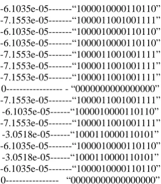
For the evaluation of the suggested design methodology a analog signal is taken and processed, the observations obtained are as illustrated below Fig.7
Fig.7 Test signal sample for observation2 Samples Considered
0--- - “0000000000000000”
-3.0518e-05---“1000110000110101”
-3.0518e-05---“1000110000110101”
0--- - “0000000000000000”
-6.1035e-05---“1000010000110110”
0--- - “0000000000000000”
-6.1035e-05---“1000010000110110”
-7.1553e-05---“1000011001001111”
-6.1035e-05---“1000010000110110”
-6.1035e-05---“1000010000110110”
-7.1553e-05---“1000011001001111”
-7.1553e-05---“1000011001001111”
-7.1553e-05---“1000011001001111”
0--- - “0000000000000000”
-7.1553e-05---“1000011001001111”
-6.1035e-05---“1000010000110110”
-7.1553e-05---“1000011001001111”
-3.0518e-05---“1000110000110101”
-6.1035e-05---“1000010000110110”
-3.0518e-05---“1000110000110101”
-6.1035e-05---“1000010000110110”
0--- “00000000000000000” The above floating point numbers corresponding plot
can be shown in below Fig.8.
Fig.8 Plot for the considered input signal sample
A.Simulation of proposed design Using ModelSim
Fig. 9 Simulation result for the implemented subband design
operation. The signal clock is passed to each filter bank for the synchronous operation
The simulation result shown above shows the global signal reset ‘rst’ passed to the system. The system is considered to be active low with the system getting activated in the lower value of the reset signal. On the initialization of the system the system get reset by applying reset as high on the first clock pulse. Under reset condition all the signal get cleared. Control signal ‘start’ is passed to the system as enable signal making the system enable whenever the signal goes high. Control signal ‘read’ is used for reading of the data stored into input-buffer. On the rising value of read signal the content of the input buffer is read and passed down to filter bank for further processing. Signal ‘sfac1’, ‘sfac2’, ‘sfac3’, ‘sfac4’ shows the scale-factors obtained for the sub-band samples. Signal ‘ebank1’, ‘ebank2’, ‘ebank3’, ‘ebank4’ gives the energy content of each sub-band sample obtained after the decomposition. The sub-band sample energy gives the energy spectral of the sub-band samples.
Fig.10 Simulation result for the implemented subband design (cont.fig.9)
Figure10 shows the simulation result for the implemented design under processing. The figure shows the signal values carried from the input buffer to the filter input via the signal tdata. The proposed design decomposes the signal into four distinct subband thus four unique temporary signals are used for the transfer of data to the filter bank. Signal fdata shows the data transferred to filter module for the processing. Sdata shows the sub-sampled data obtained for each sub-band.
Fig.11 Simulation result for the implemented subband design (cont.fig.10)
Figure11 shows the input values passed to the sub-band module. The inputs are passed to the module in Floating point Excess-7 notation. The system is passed with a clock of 100Mhz system application frequency with reset signal low as the system considered being active low. The Signal ‘start’ and ‘read’ is fed high for making the system enable and to read the data from the buffer element. The result shows the
scale factor obtained for each sub-band. The signal ‘det1’,’det2’,’det3’ and ‘app3’ gives three detailed coefficients and approximate coefficients for the input signal. Each sub-band constitute of 9 sub-samples for every packet of the data burst. The ebank’s gives the energy values of each subband sample for each subband
Figure.11 also shows the overall scale factors, detail coefficients and approximate coefficients for every packet of the signal samples. The scale factors obtained show the maximum values of the sub-band samples obtained under each subband. The energy for the samples are calculated as E=square (Magnitude of each sample).
The elements of the detailed coefficient matrix (det1) show the samples lying in the higher frequency range from 8-4KHz. The second sub-band shown by (det2) gives the coefficients lying in the range of 4-2 KHz ranges. Det3 gives the sub-samples with a frequency of 2-1KHz and app3 matrix shows the approximate coefficients lying in the range of 1-0KHz ranges
Fig.12 Output of the reconstructer module
B.Comparison of the input and output results
Figure.12 shows the ouput of the reconstructer module. If we observe figure.8 and figure12, the samples sent at the input of the decomposer module and the samples received at the ouput of the reconstructer module are same.
C.Synthesis of proposed design using Xilinx-ISE
1) Logical routing of proposed design targeting to Xc2s50e-ft256-7
Fig.13 Routing of the implemented wavelet decomposing module targeting to Xc2s50e-ft256-7
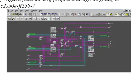
2) Logical placement of proposed design targeting to Xc2s50e-ft256-7
Fig.14 Logical placement of the implemented design in the FPGA (xc2s50e-ft256-7)
Figure14 shows the logical placement of the implemented design on to the targeted FPGA (Xc2s50e-ft256-7). The figure shows the logical resources used by the Logic implemented for the implemented design for one CLB. The basic elements used for the implementation were LUT and Buffer elements as shown in figure.
3) Floor planning of proposed design targeting to Xc2s50e-ft256-7
Fig.15 Floor planning of the implemented design in the targeted FPGA (Xc2s50e-ft256-7)
Figure15 shows the floor planning of the implemented design on to the targeted FPGA (Xc2s50e-ft256-7). The figure shows the logical net connection between the two CLB and the IO buffer used. The interconnects obtained shows the path covered for the logical mapping of the resources for data transfer for the operation.
4) Package veiw of proposed design targeting to Xc2s50e-ft256-7
Fig.16 Bottom Package View for the Target FPGA(Xc2s50e-ft256-7)
Figure16 shows the bottom view of the targeted Virtex FPGA ((Xc2s50e-ft256-7) this package view is consisting of the
power supply pins (VCC), the ground (GND) the dedicated lines used for data transfer and available pins for other applications.
Minimum period: 2.649ns
(Maximum Frequency: 377.501MHz)
Minimum input arrival time before clock: 9.656ns Maximum output required time after clock: 6.366ns Design Statistics
# IOs : 105 Cell Usage : # BELS : 205
VI.CONCLUSION
This paper outlines a design methodology for the design process of analog signal processing in digital domain. The process of filter desings approach for such a analog data is presented. A wavelet approach for a analog signal is developed as a case study to illustrate the usage of proposed design in HDL modeling. The proposed design implements a general purpose Fast Wavelet transformation system which gives rise to accurate sub-band decomposition of the signal into four distinct sub-bands. The scale factor for each subband was also obtained with the energy of each subband samples calculated. The obtained signal subabnd samples are then passed through the implemented reconstructor module which reconstruct the decomposed signal sample to a very close affinity to the original signal. From the obtained result plots it is observed that the retreived signal samples show less variation from the input. The proposed design was completely developed on ModelSim tool using VHDL language and has been synthesized on Xilinx ISE tool targeting to Virtex FPGA. The system implemented is attained for a Minimum period: 2.649ns i.e. a Maximum Frequency: 377.501MHz.
REFERENCES
[1]. M. Taher1, E. El-Araby1, A. Agarwal1, T. El-Ghazawi1, K. Gaj2, J. Le Moigne3, and N. Alexandridis1 “Effective Implementation of a Generic Wavelet Filter on a Hybrid Reconfigurable” Computer 1 The George Washington University, DC 20052 2 George Mason University, VA 22030 3NASA/Goddard Space Flight Center, Greenbelt, MD 20771.
[2]. David L. Donoho & Thomas P.Y. Yu “Robust Nonlinear Wavelet Transform based on Median-Interpolation” Department of Statistics Stanford University Stanford, CA 945305, USA.
[3]. Young HUH, Kang-Hyeon RHEE “Design of Subband Image Encoder by Discrete Wavelet Transform” Applied Imaging Research Group, KERI, Korea. School of Electronics and Info-Comm. Eng., Multimedia SoC Design Lab., Chosun University, Korea.
[4]. A.Grzeszczak, M.K.Mandal, S.Panchanathan, T.Yesp, "VLSI Implementation of Discrete Wavelet Transform", IEEE Transactions on VLSI System, Vol.4, No.4, pp 421-433, Dec 1996.
[5]. Gilbert Strang/Truong, "Wavelet and Filter Bank", Wellesley-Cambridge Press, 1996.
[6]. T.A. Ramstad S.O. Aase J.H. Husoy “Subband Compression of Image:Principles and Examples” Elsevier Science B.V, 1995
[7]. Ali N.Akansu, Mark J.T.Smith, "Subband wavelet transforms design and application", Kluwer academic publishers. 1996.
[8]. Youn-Hong Kim, Chung-Hwa Kim, Kang-Hyeon Rhee "A Design of Discrete Wavelet Transform Encoder for Image Signal Processing", Processings of IEEK Fall Conference '98. pp 1101-1104, Nov 1998. [9]. Raguveer M.Rao, Ajit S. Bopatikar “Wavelet transforms introduction to
[10]. J.Bhaskar,”AVHDL primer” Pearson education,2004.
[11] Mariantonia Cotronei, Laura B. Montefuseco, and Luigia Puccio, “Multiwavelet analysis and signal Processing”, IEEE Transactions on Circuits and system-II:Analog and Digital Signal Processing, VOL.45,NO.8.August 1998.
[12] John F.Wakerly “Digital Design” Pearson Education 2004.
[13]. Rafael C. Gonzalez, Richard E. Woods “Digital Image Processing” Addison-Wesley publishing company, 1993
[14] S.G. Mallat, “A Theory for Multiresolution Signal Decomposition: The Wavelet Representation,” IEEE Transactions on Pattern Analysis and Machine Intelligence, vol. 11, No. 7, July 1989.
[15] C.K. Chui, An Introduction to Wavelets, Wavelet Analysis and its Applications, Volume 1, Academic Press, 1992.
[16] C. Burus, et al. Introduction to Wavelets and Wavelet Transformation A Primer. Prentice Hall, 1998.
[17] K. K. Parhi, VLSI Digital Signal Processing Systems, Design and Implementation, John Wiley & Sons, NY, 1999.
AUTHORS
Mr.R.Prakash Rao, received his M.Tech degree from
Collegeof Engineering Andhra University,Vizag,India and B.Tech degree from Siddardha College of Engineering, Nagarjuna University, Guntur, India. Presently he is working as HOD in St.Peter’s Engineering College, Hyderabad. He published 06 papers in various National and International Journals and Conferences. He got best faculty award during 2009-2010 in ASTRA, Hyderabad. He has guided 02 M.Tech projects and about 25 B.Tech projects in various levels. His research interest includes VLSI,Microwave Engineering
Dr. B K Madhavi, received Ph.D from JNTU,