510 |
P a g e
VVVF POWER SOURCE USING SPWM
Apurva P. Patil
1, Sukhada Deshmukh
21
Electronics Department, R.I.T., Shivaji University , (India)
2Department of E&TC, DCOER, Pune University, (India)
ABSTRACT
VVVF power source means variable voltage variable frequency power source. Now days the development of
variable VVVF power source, is the demand for various applications. Thus the low cost variable voltage
variable frequency power source is designing using PIC micro-controller. The configuration of ac to dc
converter and dc to ac inverter is called a dc-link converter. VVVF power source is developed using MOSFET
H-bridge means full bridge inverter. Here design methodology proposed to utilize a different concept of
generating pulse width modulation signals for the driver circuit of the inverter. The PWM which is used in this
system is sinusoidal pulse width modulation (SPWM). The system proposes to incorporate the look-up table
(LUT) which will be store in the system for the sinusoidal signal generation with more stability. The proposed
system uses two micro-controllers; first micro-controller used for variable voltage & other micro-controller is
used to generate the proposed variable frequency sine wave PWM & displaying purposes. The proposed system
provides wide range of voltage and frequency commands and their performances at low cost.
Keywords
-Variable Voltage, Variable Frequency, Sinusoidal Pulse Width Modulation, PIC
Microcontroller, MOSFET H Bridge Inverter, Display.
I.INTRODUCTION
Now days dedicated types of power sources are required according to specific demands. Such requirements are
specified in form of generation of ac sources having different types of waveform shapes or variable voltages,
variable frequency of single phase or three phase power sources. So different type of power sources are
designed using different control strategy with the help of different controllers. The configuration of ac to dc
converter and dc to ac inverter is called a dc-link converter. The PWM is required for the inverter. The PWM
patterns have been achieved for different switching and fundamental frequencies. The SPWM developed in a
single FPGA. The simulations are carried out using ModelSim 5.7. [1]. Again the new method is introduced to
obtain various possible output voltages depending on the switching topology and the voltage inputs available.
This method is used to obtain a sinusoidal voltage waveform with a frequency which is a multiple of the
frequency of the sinusoidal input voltage.[2].The high precision three-phase SPWM designed which is based on
DSP chip, by using comparison units on event manager. This system provides high quality and reliability of
SPWM waveform, and output waveform of the variable frequency [3]. Using Direct Modulation Strategy the
511 |
P a g e
generated directly and thus require less memory space as compared to conventional sine-triangular scheme. The
periodic PWM signals are generated, separated by positive and negative group of polarity control switching
pulse and evoked at the output as a control signal for FPGA interfaced H bridge inverter circuit. But the direct
PWM technique scheme doesn’t using high frequency signal [4][5].
The generation of high quality variable frequency sinusoidal waveforms is designed with unique technique.
Arithmetic operations on the bit streams are performed through digital blocks. The proposed technique is simple
and can be implemented on the field programmable gate array (FPGA)[6]. Instead of this if PIC controllers are
used then cost will be reduce. So I am trying to design the low cost, stable & reliable power source at desired
voltage & desired frequency.
II.SYSTEM DESCRIPTION
The block diagram describes the development of a microcontroller-based single phase Variable Voltage
Variable Frequency (VVVF) sinusoidal power source. The proposed scheme uses the new different concept of
generating PWM signals, called sinusoidal pulse width modulation (SPWM) signals. In SPWM technique, sine
wave is compare with triangular wave, the frequency of triangular wave describes number of pulses in output
for each half cycle. The width of PWM is varied with respect to amplitude of sine wave means the pulse width
is made sinusoidal function of angular position of pulse in the cycle. In this system SPWM is generated with the
help of look-up table (LUT). The system uses two microcontrollers where one micro-controller is used to
generate the proposed variable voltage and the other micro-controller is used for controlling the frequency &
LCD display. The variable voltage & variable frequency are display on the LCD.
Fig.1 Block Diagram of Proposed System
AC voltage having 230V, 50Hz from the mains is applied to the step down transformer then it rectified. The
resistive pot is connected to the PIC controller. With the help of pot the voltage is varied. The controlled signal
512 |
P a g e
bridge rectifier; rectifier converts this AC into DC. This DC voltage is as an input voltage for an inverter. The
full bridge inverter is constructed with the four N channel enhancement MOSFETs. The second PIC controller is
used for the generation of SPWM & the pot is connected to this controller. The frequency can be varied with
respect to this pot. The SPWM pulses are required for firing the MOSFETs. The inverter is used to convert this
DC voltage in to AC again. After that bulb is used as the load to the circuit. The output ac voltage is again step
down and rectified. And it gives to PIC controller for displaying purpose. The output voltage and frequency will
be display on LCD display.
III.DESIGN OF THE HARDWARE
The hardware is design with the help of PIC controller, TRIAC, BridgeKBPC3510, MOSFETs, MOSFET
Drivers, and MOSFETs.
3.1 PIC controller
In this system I am using 16F877A. It is 40 pins high performance RISC CPU. It operate on 2.0V to 5.5V rang.
It provides inbuilt 10 bit ADC with 8 channels. It has 256 B Data ROM. It has up to 18 sources interrupt
capability & three timers.
3.2 TRIAC
These are three terminal devices. BTA41 is a TRIAC having 800V peak off-state voltage& 41A on-state rms
current. With the help of TRIAC we can control the AC.
3.3 MOSFETs
MOSFETs are required for single phase full bridge inverter. IRFP460 is the MOSFET which is used in this
system. For the fast switching purpose IRFP460 is used. Its Drain-Source voltage is 500V and continuous drain
current is 20A. MOSFET drivers are required for the IRFP460.
3.4 MOSFET Drivers
IR2110 is used in the present system. MOSFET Drivers are required to drive an N-channel power MOSFET in
the high-side configuration which operates up to 500 V. Its Gate drive supply range is 10 to 20V.This can drive
independently high and low-side referenced output channels.
IV.DEVELOPMENT OF THE SOFTWARE
In this system author using two microcontrollers. First for variable voltage and second for generation of SPWM.
The first controller controls the firing angle of triac. The pot is provided for varying the firing angle. When pot
varies that time ADC convert the analog data and according to that firing angle is provided to triac. And using
this technique we are converted the AC in to controlled AC signal.
The second controller controls the operation of an inverter. The PWM is the heart of an inverter. In this system
SPWM signal is generated which will provide to the MOSFETs. For this purpose look-up table will generate
and store in the system. Total 80 steps are generated for each half cycle. For variable frequency purpose pot is
connected. According to pot position frequency will change and values will be call from look up table. The
513 |
P a g e
V.EXPERIMENTAL RESULTS
The center tap rectifier is used in this system. The signal after rectification is shown in fig. 2(a). And fig.
2(b) shoes zero crossing signal. Whenever the signal of rectifier crosses the zero that time we get the pulses
as shown in fig 2(b).
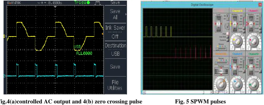
Fig.2(a) Rectified signal and 2(b)Zero crossing signal Fig.3(a) Zero crossing signal and 3(b) Triac firing signal
The zero crossing signals are shown in figure 3(a). The difference between two zero crossing pulses is
10ms. The triac firing pulses are generated with the help of PIC controller. When the pot will vary that time
firing angle of triac will change. T he firing pulses for triac with respect to zero crossing are shown in Fig.3
(b). Here triac is fire at 4ms. Fig. 4 shows the controlled AC signal with respect to controlled pulses from
controller.
Fig.4(a)controlled AC output and 4(b) zero crossing pulse Fig. 5 SPWM pulses
The second controller is used to generate the SPWM. The 80 step size per half cycle is selected for more
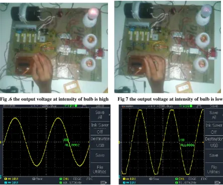
accuracy. Fig.5 shows the SPWM pulses which are generated by CCP modules. Fig. 6 and 7 shoes the output of
the system. The firing angle of triac is changes according to that the intensity of bulb which is connected to the
output side is change. Fig. 6 shows the high intensity of bulb and that time the output voltage is 61V. Fig. 7
shows the low intensity of bulb at 41V. The final output is step down and sense by the controller.
Fig. 8 show output waveform having 40Hz frequency and fig.9 show the 51 Hz’s waveform. Fig.10 shows the
514 |
P a g e
Fig .6 the output voltage at intensity of bulb is high Fig 7 the output voltage at intensity of bulb is low
Fig 8 output sine wave at 40 Hz Fig 9 output sine wave at 51Hz
Fig 10LCD display
VI. CONCLUSION
In this work the VVVF power source is design using microcontroller at low cost. The configuration of ac to dc
converter and dc to ac inverter is called a dc-link converter. This system is also the DC-link. As compare to DSP
controller the cost of PIC controller is less. This system will provide more stable, reliable output because of the
515 |
P a g e
VII. ACKNOWLEDGEMENT
The authors would like to thank the Rajarambapu Institute of Technology for the timely and important help. The
authors also wish to thank the reviewers for their very detailed review of the manuscript and for their help.
REFERENCES
[1] R. K. Pongiannan1, Member- IEEE, P. Selvabharathi2, N. Yadaiah, Sr. Member-IEEE ―FPGA Based
Three Phase Sinusoidal PWM VVVF Controller‖, First International Conference onElectrical Energy
Systems (ICEES),Page(s): 34 - 39 , 2011 IEEE.
[2] A. Salimi, S.Mansourpour, H.Ziar, E.Afjei, ―A Simple and Novel Modulation Technique Used to Obtain Output Voltage Having a Frequency Multiple of Input Voltage Frequency‖,2011 International Aegean
Conference on Electrical Machines and Power Electronics and 2011 Electromotion Joint Conference
(ACEMP). Page(s): 596 - 600, 2011.
[3] Lin Chengwu,Liu Yan, Sun Bingbin,―Study On The Technology Of Inverter Based On DSP And SPWM‖,International Conference onAutomatic Control and Artificial Intelligence (ACAI 2012). Page(s):
1993 – 1995, 2011.
[4] MrigankaSekhar Sur , S. N. Singh, Anumeha, PuspaKumari, ―Simulation And Generation Of SPWM
Waveform Using VHDL For FPGA Interfaced H Bridge Power Inverter‖, 2010 IEEE paper of International Conference on Industrial Electronics, Control and Robotics.Page(s): 39 – 42, 2010.
[5] Lin Jiaquan, Pi Jun ,―A New Scheme of VVVF Inverter Using Line Voltage Direct PWM‖, The Ninth
International Conference on Electronic Measurement &Instruments,Page(s): 3-633 - 3-637,2009. [6] N.
D. Patel and U. K. Madawala ,―A Bit-Stream Based PWM Technique for Variable Frequency Sinewave Generation‖, The Thirteenth Conference onPower Electronics and Motion Control Conference,