IJEDR2001024 International Journal of Engineering Development and Research (www.ijedr.org) 125
Adiabatic Logic Modelling using VHDL
1Shiwani Singh, 2Sonam Rathore 1Assistant Professor, 2Assistant Professor
1Shri Ram Murti Smarak College of Engineering, Technology & Research, Bareilly, 2Shri Ram Murti Smarak College of Engineering, Technology & Research, Bareilly
_____________________________________________________________________________________________________
Abstract - Adiabatic circuits are low power circuits which use reversible logic to conserve energy. Unlike traditional CMOS circuits, which dissipate energy during switching, adiabatic circuits reduce dissipation by never turning on a transistor when there is a voltage potential between the source and drain and never turning off a transistor when current is flowing through it. The verification of the functionality and the low energy traits of adiabatic logic techniques are generally performed using transient simulations at the transistor level. However, as the size and complexity of the adiabatic system increases, the amount of time required to design and simulate also increases. Moreover, due to the complexity of synchronizing the power-clock phases, debugging of errors becomes difficult too thus, increasing the overall verification time. Using the proposed approach, the functional errors can be detected and corrected at an early design stage so that when designing adiabatic circuits at the transistor level, the circuit performs correctly and the time for debugging the errors can substantially be reduced. The function is defined using a library containing the behavioral VHDL models of adiabatic domino XOR logic gate. Finally, this library is used to develop and verify the structural VHDL representation of a full adder, as a design example that demonstrates the practicality of the proposed approach. This paper proposes a VHSIC Hardware Descriptive Language (VHDL) based modelling approach for developing models representing single phase adiabatic logic designs.
keywords - Adiabatic logic, domino, low power, XOR, adder and VHDL
_____________________________________________________________________________________________________
I.INTRODUCTION
The use of adiabatic logic technique instead of the nonadiabatic logic design can considerably decrease the energy consumption in a large system. Though it is in existence for more than two decades, still, its full potential has not been explored. However, various research papers demonstrated the energy saving potential of the adiabatic logic technique compared to the non-adiabatic logic. In [2], it has been shown that at lower technology nodes adiabatic logic has better energy performance than nonadiabatic logic. Similarly, in [3] the behavior of adiabatic logic circuits in weak inversion or subthreshold regime is analyzed. Through extensive post-layout simulation, it demonstrated that subthreshold adiabatic circuits can save significant energy compared with an equivalent non-adiabatic implementation. Moreover, the recent work of adiabatic principle applicability to adiabatic capacitive logic demonstrate the effectiveness of the technique to achieve zero-power logic dissipation [4]. Nevertheless, the functional verification of the adiabatic design at the transistors level is time-consuming and difficult.
The design of adiabatic circuits requires much more efforts in contrast to the non-adiabatic logic for which well-developed tools exist. The major difference between the two is that the adiabatic logic designs use slowly changing AC power-clock supply instead of DC (constant) power-supply. VHDL is valid and is efficiently used for signal levels ‘0’ and ‘1’ having zero rise and fall times for ideal simulations. However, in adiabatic logic, waveforms are more complex because of the multi-phase clocking and the dual-rail encoding of inputs and outputs. Thus, in addition to logic ‘1’ and logic ‘0’, the adiabatic power-clock supply uses two more logic levels where the power-clock transition is a ramp such that all the four levels share the same period. Based on the literature review, the first modelling in VHDL of adiabatic logic was done by M. Vollmer and J. Gotze in 2005. They described the adiabatic logic in VHDL for a systolic array with precise timing and bit-true calculation [5]. Their work included the description of logic blocks that required 4-phase clocking scheme but did not model the dual rail encoding and use one global clock net instead of 4-phase power-clock for cascade designs. A year later, Laszlo Varga et.al, described two-level pipelining scheduling of adiabatic logic using integer linear programming formulation and a heuristic scheduling [6]. The authors presented the VHDL description for functional simulation of the synthesized adiabatic data path together with the non-adiabatic part of the digital system. This approach focusses mainly on producing a pipeline schedule of the power-clock behaviour of the adiabatic logic but did not model the power-clock and the dual-rail behaviour of the adiabatic logic. In 2010, David John Willingham in his PhD thesis [7] reported Asynchrobatic Logic in Verilog, an industry standard Hardware Description Language (HDL). First, the author demonstrated the idea in a single-rail scheme and then extended it to dual-rail, which was found to be missing in Vollmer and Laszlo’s modelling. The dual-rail implementation proves to be advantageous in detecting an invalid circuit operation to some extent. The author defined three states namely; valid state (logic ‘1’ or logic ‘0’), invalid state and inactive state. This approach also did not model the power-clock in HDL, instead, it used square waves for generating the 4-phase power-clock. Though all were able to demonstrate the pipeline timing, none followed the adiabatic principles, that is, the circuit generates valid output signal when the input and the power-clock are both in the same phase. Moreover, the square-wave used as a power-clock evaluation and hold.
IJEDR2001024 International Journal of Engineering Development and Research (www.ijedr.org) 126 complementary outputs. The modelling includes the dual-rail representation of the input/output signals. The paper is structured as follows; Section II describes the existing domino XOR gate and full adder. Section III shows how the precise timing of the proposed VHDL modelling is captured along with the comparison and validation of the proposed VHDL modelling with SPICE simulation results followed by conclusion in section IV.
II.EXISTING XOR GATE AND FULL ADDER CELL
Fig.1 Domino logic based XOR Gate
The schematic of domino XOR cell is shown in Fig. 1. This circuit overcomes the problems occurred in existing XOR cell. The source terminal of pMOS transistor P1 and drain terminal of nMOS transistor N1 are connected to VDD. The transistor P1 is used as precharge transistor while N4 is used as footer transistor. Single clock signal is used to drive both of these transistors in each dynamic stage. Instead of connecting pMOS as keeper transistor, nMOS transistor N1 is connected in parallel with transistor P1 so that inverting functions can also be implemented in domino design techniques. This eliminates the need of another inverter for generating inverted functions [1]. And thus, both XOR and XNOR gates can be implemented in single design. Two nMOS transistors N6 and N7 are also added to obtain correct output for combinations AB=11. The current mirror as given in literatue[8] has been removed as this part was only consuming area and in turn gives increased power consumption of the design.
The circuit operation takes place in two phases i.e. precharge phase and evaluation phase. In precharge phase, clock signal is low. P1 will turn on. Footer transistor N4 is turn off. Dynamic node V1 is charged to high voltage by pull up transistor. Now keeper transistor N1 will turn on to keep dynamic node at high voltage level and overcome charge sharing effect. In precharge phase input signal will not affect the output. There is no discharging path between dynamic node and ground. Therefore we get low voltage at output node. Table I depicts the performance of both existing and proposed designs.[21]-[25]. From the table it is clear that proposed circuitry has shown improved threshold loss and verifies the logical expression of XOR gate as compared to existing one.
In evaluation phase, clock signal is high, the pull-up transistor P1 and N1 will turn off and footer transistor N4 will turn on. This phase is further divided in four cases. Here, charging or discharging of the dynamic node is depending upon input signals.
Case 1: When both input signals are low i.e. A=B=0, P2 and P3 turn on in pull down network and rest will be in off state. There is no conducting path between dynamic node and ground to discharge the dynamic node voltage. So, it will remain at high logic. Therefore, get low logic at output.
Case 2: When both input signals are at different logic state, i.e. A=0 and B=1, it will turn on the series connection of transistor N3 and P3 of pull down network. Now there will be a conducting path between VDD and ground. This will discharge the dynamic node and get high logic at the output node.
Case 3: When A=1 and B=0, it will turn on the series connection of transistor N2 and P2 of pull down network. Now again there will be a conducting path between VDD and ground. This will discharge the dynamic node and get high logic at the output node.
IJEDR2001024 International Journal of Engineering Development and Research (www.ijedr.org) 127
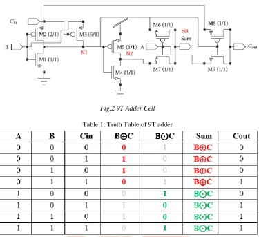
Fig.2 9T Adder Cell
Table 1: Truth Table of 9T adder
The schematic of 9T full adder cell is shown in Figure 2 and its truth table is stated in Table 1. The operating principle of proposed circuit is different from traditional circuits. For generating the Sum output in the proposed design, the truth table has been divided into two parts, one for input A = “0” and another for A = “1” rather than implementing the conventional Sum module of (1). From the truth table shown in Table 1 it is evident that when A = “0”, Sum can be produced by XORing inputs B and Cin. Similarly, when A = “1”, Sum is showing the XNORing between inputs B and Cin. Therefore, the operation of Sum module is based on implementing XOR operation and XNOR operation between inputs B and Cin. The logic for Cout output is also stated. The equations for same are stated as:
For Sum, When A=0, Sum=B⊕Cin. When A=1, Sum=not(B⊕Cin)
For Cout, When B⊕Cin = 0, Cout=Cin. When B⊕Cin=1, Cout=A.
An inverter is connected at the output of first-stage XOR gate to generate XNOR function. Finally the Sum is implemented by transferring these output levels through 2T multiplexer. Input to the PMOS (M6) of 2T multiplexer is XOR of B and Cin while to NMOS (M7) is XNOR of B and Cin. This 2T multiplexer is controlled by input A. Cout is implemented by using another 2T multiplexer which is controlled by output of first-stage XOR gate and passes either A or Cin accordingly. This circuit reduces the overall PDP at varying input voltages and operating frequencies and also improves the temperature sustainability while operating in subthreshold region.
III.PROPOSED WORK
One of the advantages of HDL modelling is that the design can be simulated with logic simulators and can be interfaced and mixed with the non-adiabatic logic designs for effective design solutions. Apart from modelling the power-clock, the adiabatic inputs must also be modelled for proper interfacing and correct functionality. The trapezoidal power-clock used at the transistor level is first encoded in standard logic to capture the timing behaviour of the adiabatic logic. This is followed by interconnection modelling (pulse input to adiabatic conversion) and gate-level modelling.[15],[17],[19].
IJEDR2001024 International Journal of Engineering Development and Research (www.ijedr.org) 128 an invalid input, which the SPICE simulations and the previously defined modelling approaches in the open literature fail to identify. The more detailed analysis of modelling an invalid state accurately is given in the next subsection.
The adiabatic logic technique is one of the innovative solutions at logic and circuit level to achieve a reduction in energy dissipation for devices working at less than 100MHz frequency. The adiabatic circuits would operate ideally with zero dissipation that may be approached as the logic switching is slowed down. A decreased energy dissipation with increased switching time is, therefore, the defining property of an adiabatic switching [9]-[11]. The use of a slowly changing power-clock which allows approximately constant current charging/discharging helps in avoiding the current surges and therefore, the circuit dissipates less energy [9]. In addition, this slowly charging process gives an additional advantage of pumping the stored energy back to the power supply during the discharging process which can be recovered using an AC power-clock generator. The detailed derivation of (1) is given in [10].
ED= (RCL/Tr) CLVDD2
Where ED is the energy dissipation, Tr is the ramping time, CL is the effective output load capacitance, R is the charging path resistance and VDD is the supply voltage.
It should be noted that the above equation doesn’t take into account the energy loss due to leakage and threshold voltage degradation (non-adiabatic loss) Fig. 1 shows the input and the 4-phase power-clock with each phase having 90o of phase difference with each other. The 4-phase power-clocks are broken down into four equal time periods namely evaluation (E), hold (H), recovery (R) and idle (I). To have less energy dissipation, all the nodes in a circuit should share the same principle of charging and discharging. For example, in cascade logic, during the evaluation period of the power-clock (PC1), the input which is being sampled must be stable for the stage to produce a valid output in the hold period. The second stage will be sampling its input while the output of the first stage is stable (hold period) and so on. This behavior forms a pipeline, processing one input and one output at every power-clock phase.
The single-phase adiabatic logic is implicitly pipelined and glitch-free. This suggests that there is no concern about the critical paths. However, in a large adiabatic system using power-clocking scheme, the debugging of errors are time-consuming due to the complexity of synchronizing the power-clock phases. The difficulty of modelling the adiabatic logic accurately arises due to the trapezoidal shape of the AC power-clock. Thus, to model the adiabatic behavior using HDL, the first task is to conceptualize the trapezoidal AC power-clock behavior using HDL. Then writing the behavioral code of the basic logic gates for functional and timing verification. The multi-level event-based approach is proposed for modelling the four equal time-periods of a trapezoidal AC power-clock. In this method, the hold and idle periods of the power-clock are represented as logic ‘1’ and logic ‘0’ respectively. Whereas, the evaluation and the recovery period are encoded with an intermediate state marked as ‘X’, as both share the same duration of the ramp period[9]-[13]. This approach is not straightforward, as apart from generating the power-clock which has three logic levels, the adiabatic inputs must also be generated with three logic levels for proper functionality and timing analysis.
Our proposed VHDL model can easily identify the errors caused by the complementary inputs when both are at logic ‘0’, which the SPICE simulation fails to identify. In this case, the circuit remains inactive, that is, the complementary output voltages remain at logic ‘0’, detecting an invalid input condition. Similarly, when the complementary inputs are at logic ‘1’, the complementary output nodes remain at a high impedance state encoded by ‘Z’. Thus, two different states, ‘0’ and ‘Z’ are used when the complementary inputs are driven to the same logic values (invalid conditions). This helps in identifying the value of the invalid inputs precisely
IJEDR2001024 International Journal of Engineering Development and Research (www.ijedr.org) 129
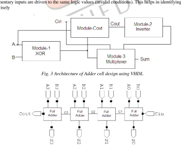
Figure 4: Block Diagram of 4 bit RCA
VHDL behavior is described by combining the functional part and the adiabatic XOR/MUX for timing validation. The collection of all the logic gates described in VHDL formed the cell library. Using the homegrown cell library, the structural models of a 4-bit RCA is also were successfully verified as shown in figure 5. The circuit functionality and timing verification were done using Xilinx. The time period of the power-clock was taken as 100ns, having equal time for the four periods of the powerclock i.e. 25ns each. The simulation setup for VHDL is similar to that of SPICE so that uniformity and comparability are maintained across both the simulations.
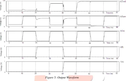
The waveform for simulated adder cell is shown in following figure 5.
Figure 5: Output Waveform
The graph shown in Fig. 6 reveals that the power consumption of proposed design is 20% to 98% reduced than the existing one but the delay of proposed cell is slightly more than that of existing design for the input voltage 0.5V and 0.6V but the curve of delay is decreasing with increase in input voltage. This decrease in delay is because of the inverse relationship between power and delay with respect to voltage. As depicted the decrease in power consumption and delay results into 20% to 51% reduced PDP for the proposed design.
Figure 6: Power comparison of adder circuit
IV.CONCLUSION
IJEDR2001024 International Journal of Engineering Development and Research (www.ijedr.org) 130 validate of a large complex system, eventually reducing the amount of time needed for synchronizing and detecting design errors.
REFERENCES
[1] G. Yemiscioglu, & P. Lee, “Very-large-scale integration implementation of a 16-bit clocked adiabatic logic logarithmic signal processor”, IET Computers & Digital Techniques, Vol. 9, pp.239–247,2015.
[2] V. S. K. Bhaaskaran, "Energy recovery performance of quasi-adiabatic circuits using lower technology nodes,"India International Conference on Power Electronics, pp. 1-7,2011.
[3] M. Chanda, S. Jain, S. De and C. K. Sarkar, "Implementation of Subthreshold Adiabatic Logic for Ultralow-Power Application," in IEEE Transactions on Very Large Scale Integration (VLSI) Systems, Vol. 23, No.12, pp. 2782-2790, 2015. [4] G. Pillonnet, H. Fanet and S. Houri, "Adiabatic capacitive logic: A paradigm for low-power logic,"IEEE International Symposium on Circuitsand Systems (ISCAS), pp. 1-4,2017.
[5] M. Vollmer, and J. Götze, "An adiabatic architecture for linear signal processing", Advances in Radio Science, pp.325–329, 2005.
[6] L. Varga, G. Hosszu and F. Kovacs, "Two-level Pipeline Scheduling of Adiabatic Logic," 2006 29th International Spring Seminar on Electronics Technology, St. Marienthal, pp. 390-394,2006.
[7] David John WILLINGHAM, “Asynchrobatic logic for low-power VLSI design,” PhD. Thesis, 2010.
[8] E. Amirante, A. Bargagli-Stoffi, J. Fischer, G. Iannaccone and D. Schmitt-Landsiedel, “Variations of the Power Dissipation in Adiabatic Logic Gates,” International Workshop on Power and Timing Modelling, Optimization and Simulation (PATMOS), pp.9.1.1–9.1.10, 2001.
[9] J. G. Koller and W. C. Athas, “Adiabatic Switching, Low Energy Computing”, and the Physics of Storing and Erasing Information, Proc. of the 2nd Workshop on Physics and Computation,pp.267-270,1992.
[10] W. C. Athas, L. J. Svensson, J. G. Koller, N. Tzartzanis and E. YingChin Chou “Low-Power Digital Systems Based on Adiabatic switching Principles”, IEEE Tran. on VLSI Sys., Vol. 2, No. 4,pp.398-407, 1994.
[11] J. S. Denker, “A review of adiabatic computing,” IEEE Symposium on Low Power Electronics – Digest of Technical Papers,pp.94-97,1994.
[12] Himadri Singh Raghav, V. A. Bartlett, and I. Kale, “Investigation of stepwise charging circuits for power-clock generation in Adiabatic Logic”, 12th Conference on Ph.D. Research in Microelectronics and Electronics(PRIME), pp. 1-4,2016.
[13] Himadri Singh Raghav, V.A.Bartlett and Izzet Kale, “Energy efficiency of 2-step charging power-clock for adiabatic logic”, International Workshop on Power and Timing Modelling, Optimisation and Simulation(PATMOS),pp. 176-182, 2016. [14] L. Svensson, J. Koller, Driving a capacitive load without discharging fCV^2, in: Proceedings of the IEEE Symposium on Low-power Electronics,1994, pp. 100–103.
[15] Athas, W. C., Koller, J. G., and Svensson, L, “An Energy-Efficient CMOS Line Driver Using Adiabatic Switching”, Proc. of IEEE Great Lakes Symposium on VLSI, 1994.
[16] Sachin Maheshwari, Viv A. Bartlett, I. Kale, “4-phase resettable quasiadiabatic flip-flops and sequential circuit design”, 12th Conf. on Ph.D. Research inMicroelectronicsand Electronics (PRIME), pp. 1-4, 2016.
[17] Sachin Maheshwari, V.A.Bartlett and Izzet Kale, “Adiabatic Flip-Flops and Sequential Circuit Designs using Novel Resettable Adiabatic Buffers”, European Conf. on Circuit Theory and Design (ECCTD), pp. 1-4, 2017.
[18] A. Vetuli, S. Di Pascoli, and L. Reyneri, “Positive feedback in adiabatic logic,” Electronics Letters, vol. 32,no. 20, pp. 1867–1868,1996.
[19] Philip Teichmann. Adiabatic logic: future trend and system level perspective, Springer Science & Business Media, vol. 34, pp. 10-14, 2011.
[20] Ph. Teichmann, M. Vollmer, J. Fischer, B. Heyne, J. G€otze, D. Schmitt-Landsiedel, “Saving potentials of adiab, in: Logic on System Level: a CORDIC-based Adiabatic DCT”, 12th International Symposium on Interated Circuits,pp.105–108,2009. [21] M.C. Knapp, P.J. Kindlmann, M.C. Papaefthymiou, “Design and evaluating of adiabatic arithmetic units”, Analog Integr. Circuits Signal Process, vol. 14,71–79,1997.
[22] J. Fischer, E. Amirante, F. Randazzo, G. Iannaccone, D. SchmittLandsiedel, “Reduction of the energy consumption in adiabatic gates by optimal transistor sizing”, International Workshop on Power and Timing Modelling, Optimisation and Simulation (PATMOS), pp. 309–318, 2003.
[23] Shiwani Singh, Tripti Sharma, K.G.Sharma and Prof.B.P.Singh, “New Improved 1-Bit 9T Full Adder Cell”, Proceedings of International Conference on VLSI, Communication and Networks, IET Alwar, pp. 78-81, Dec 24-25, 2011.
[24] Tripti Sharma, Shiwani Singh, K.G.Sharma and Prof.B.P.Singh, “New 9T Full Adder Design with 30% Reduced Threshold Loss”, Int. J. on Recent Trends in Engineering and Technology, Vol. 6, No. 2, pp. 279-281, Nov 2011.