Structures
by
Kyle Jackman
Dissertation presented for the degree of Doctor of
Philosophy in Electrical and Electronic Engineering in the
Faculty of Engineering at Stellenbosch University
Supervisor: Prof. Coenrad J. Fourie
Electrical and Electronic Engineering Stellenbosch University
Marc 2018
The financial assistance of the National Research Foundation (NRF) towards this research is hereby acknowledged. Opinions expressed and conclusions arrived at, are those of the author and are not necessarily to be attributed to the NRF.
Declaration
By submitting this dissertation electronically, I declare that the entirety of the work contained therein is my own, original work, that I am the sole author thereof (save to the extent explicitly otherwise stated), that reproduction and publication thereof by Stellenbosch University will not infringe any third party rights and that I have not previously in its entirety or in part submitted it for obtaining any qualification.
This dissertation includes one original paper published in peer-reviewed journals or books and 0 unpublished publications. The development and writ-ing of the papers (published and unpublished) were the principal responsibility of myself and, for each of the cases where this is not the case, a declaration is included in the dissertation indicating the nature and extent of the contribu-tions of co-authors.
Signature: K. Jackman
Date: 2017/10/27
Copyright © 2018 StellenboschUniversity All rights reserved.
Abstract
Fast Multi-Core CEM Solvers and Flux Trapping
Analysis for Superconducting Structures
K. Jackman
Department of Electrical and Electronic Engineering, University of Stellenbosch,
Private Bag X1, Matieland 7602, South Africa. Dissertation: PhD
October 2017
The dissertation presents the development of a numerical field solver, called TetraHenry (TTH), for inductance extraction and flux trapping analysis of superconducting integrated circuits. The solver uses tetrahedral elements to model multidirectional current flow in complex three-dimensional supercon-ducting volumes; whereas two dimensional triangular elements are used for sheet currents in thin superconducting films. Triangular meshing significantly reduces the number of unknowns and provides the capability to analyse chip-scale superconducting layouts. Support for piecewise homogenous dielectric materials are implemented, which enables frequency-depended impedance ex-traction. The Fast Multipole Method for the Biot-Savart law, which enables the simulation of magnetic materials, is derived. The effects of external mag-netic fields on the performance of superconducting circuits are analysed. The amount of flux through each hole or moat can be specified using the Volume Loop basis function; enabling flux trapping analysis and inductance extrac-tion around holes. The full derivaextrac-tion of the integral equaextrac-tions for volume and sheet currents are discussed. The Method of Moments is used to obtain a system of linear equations, which is solved with a preconditioned GMRES solver. Matrix-vector multiplication is accelerated with the Fast Multipole method. The accuracy and performance of the numerical solver are evaluated, by comparing simulated results to existing software.
Uittreksel
Vinnige Multi-Kern Elektromagnetiese Veldoplosser en
Vloed-Vasvang Analise vir Supergeleidende Strukture
(“Fast Multi-Core CEM Solvers and Flux Trapping Analysis for Superconducting Structures”)
K. Jackman
Departement Elektriese en Elektroniese Ingenieurswese, Universiteit van Stellenbosch,
Privaatsak X1, Matieland 7602, Suid Afrika. Proefskrif: PhD
Oktober 2017
Die dissertasie bied aan die ontwikkeling van ’n numeriese veldoplosser, ge-naamd TetraHenry (TTH), vir induktansie onttrekking en vloed-vasvang ana-lise van supergeleier geïntegreerde stroombane. Die veldoplosser gebruik tetra-hedraal elemente om stroomvloei binne komplekse driedimensionele supergelei-dende volumes te modelleer; terwyl tweedimensionele driehoekige elemente ge-bruik word vir stroomvloei in dun supergeleier filamente. Driehoekige elemente verminder die aantal onbekendes aansienlik en bied die vermoë om supergeleier uitlegte op groot skaal te analiseer. Ondersteuning vir stuksgewyse homogene diëlektriese materiale word geïmplementeer, wat frekwensie-afhanklike impe-dansie onttrekking moontlik maak. Die “Fast Multipole” metode vir die Biot Savart wet, wat die simulering van magnetiese materiale moontlik maak, word afgelei. Die effekte van eksterne magnetiese velde op supergeleier stroombane word ontleed. Vloed-vasvang analise en induktansie onttrekking rondom gate word uitgevoer met behulp van Volume Lus funksies. Die volledige afleiding van die integraalvergelykings vir volume en oppervlakstrome word bespreek. Die Metode van Momente word gebruik om ’n stelsel van lineêre vergelykings te verkry, wat opgelos word met ’n voorafbepaalde GMRES iteratiewe oplos-ser. Matriks-vektor vermenigvuldiging word versnel met die “Fast Multipole” metode. Die akkuraatheid en spoed van die numeriese enjin word geëvalueer deur gesimuleerde resultate te vergelyk met bestaande sagteware.
Acknowledgements
I would like to express my sincere gratitude to the following people:
I am most grateful to my supervisor, Professor Coenrad J. Fourie. Thank you for all the expert advice and support through the last four years. Thank you for introducing me to the field of applied superconductivity, for teaching me the fundamentals in superconducting circuits, and taking me to various international conferences. I could not have wished for a better supervisor.
To Ruben Van Staden and Johannes A. Delport, thank you for all the motivational speeches and support through the last four years.
To Professor Pascal Febvre, thank you for your expert advice on Josephson Junctions.
I am also grateful to the National Research Foundation (NRF) for financing my post-graduate studies.
Lastly, I want to thank my parents. Without your love, support and un-derstanding I could not have achieved what I have.
Contents
Declaration i Abstract ii Uittreksel iii Acknowledgements iv Contents vList of Figures viii
List of Tables xiii
1 Introduction 1
1.1 Motivation . . . 1
1.2 Inductance Extraction . . . 2
1.3 Objectives of dissertation . . . 3
2 3D Tetrahedral Modelling Method 6 2.1 Introduction . . . 6
2.2 Background Formulation . . . 6
2.3 Derivation of Volume Integral Equation . . . 7
2.3.1 Superconductivity . . . 9
2.3.2 Discretization . . . 10
2.3.3 Volume loop basis function . . . 13
2.3.4 Fundamental Set of Basis Functions . . . 15
2.3.5 Port Excitations . . . 17
2.4 Resistance and Inductance Matrices . . . 18
2.4.1 Resistance Matrix . . . 19
2.4.2 Electrostatic Analogy . . . 20
2.4.3 Solving Double Integrals . . . 22
2.5 Iterative Solver . . . 24
2.5.1 GMRES . . . 25
2.5.2 Preconditioning . . . 25
2.6 Meshing . . . 29
2.6.1 Modeling Penetration Depth . . . 30
2.7 Results . . . 32
2.7.1 Small Superconducting Structures . . . 32
2.7.2 Coupling Between Two Moats . . . 33
2.7.3 Large-scale Superconducting Circuits . . . 34
2.7.3.1 Coupling between moats and inductors . . . . 35
2.8 Conclusion . . . 40
3 2D Triangular Modelling Method 41 3.1 Introduction . . . 41
3.2 Derivation of Surface Integral Equation . . . 41
3.2.1 Discretization . . . 43
3.2.2 Surface loop basis function . . . 45
3.3 Numerical integration . . . 46
3.4 Results . . . 47
3.4.1 Single-Layer Superconducting Films . . . 47
3.4.2 Multi-Layered Superconducting Films . . . 48
3.5 Hybrid Meshes . . . 51
3.6 Conclusion . . . 53
4 Inhomogeneous Dielectric and Magnetic Materials 54 4.1 Introduction . . . 54
4.1.1 Impedance Extraction . . . 54
4.1.2 Magnetic Materials . . . 56
4.2 Obtaining Volume Integral Equations . . . 57
4.2.1 Maxwell’s equations . . . 57
4.2.2 Volume Equivalent Principle . . . 58
4.2.3 Volume Integral Equations . . . 59
4.3 VJIE and the Half-SWG Function . . . 60
4.3.1 Potential Fields . . . 62
4.3.2 Obtaining Linear Set of Equations . . . 63
4.3.3 Volume Loop Basis Functions with Half-SWG . . . 64
4.3.4 Multiple Dielectrics . . . 66
4.4 Solving the Linear System . . . 67
4.4.1 Preconditioner . . . 67
4.5 Impedance Extraction . . . 69
4.5.1 EMQS Analysis . . . 69
4.5.1.1 Copper Spiral in Free-Space . . . 69
4.5.2 Full-Wave Analysis . . . 70
4.5.2.1 Transmission Line in Free-Space . . . 71
4.5.2.2 Probe-Fed Patch Antenna . . . 72
4.5.3 Superconducting Transmission Line with Vias . . . 73
4.6.1 Permeable cylinder . . . 77
4.6.2 Coil Above Permeable Substrate . . . 80
4.6.3 Superconducting Microstrip Line with Permeable Sub-strate . . . 82
4.6.4 Inductive Coupling Using Permeable Layer . . . 84
4.7 Conclusion . . . 87
5 External Magnetic Field 88 5.1 Introduction . . . 88
5.2 Implementing Magnetic Fields . . . 88
5.2.1 Superconducting Washer in External Magnetic Field . 91 5.2.2 Penetration Depths of Superconducting Slab . . . 92
5.3 Equivalent Circuit Model for Magnetic Field . . . 94
5.3.1 Superconducting Washer in Magnetic Field . . . 96
5.3.2 SFQ Pulse Splitter in Magnetic Field . . . 96
5.4 Conclusion . . . 100
6 Fast Multipole Method for Biot-Savart Law 101 6.1 Introduction . . . 101
6.2 Far-Field Approximation . . . 102
6.2.1 Multipole Expansion . . . 102
6.2.2 Local Expansions . . . 103
6.3 Real Coeficient Multipole Algorithm . . . 104
6.3.1 Multipole Expansion Matrices (Q2M) . . . 105
6.3.2 Local Expansion Matrices (Q2L) . . . 106
6.4 Implementation of FMM Algorithm . . . 107 6.5 Numerical Results . . . 108 6.6 Conclusion . . . 113 7 Conclusion 114 Bibliography 116 Appendices 127
A Journal Paper - Flux Trapping Analysis 128 B Conference Paper - Fast FastHenry (FFH) 134
List of Figures
2.2.1 Two conductors with sinusoidal excitation voltages at given frequency. 7 2.3.1 Full-SWG basis functions in arbitrary body with piecewise constant
electrical parameters. . . 10
2.3.2 Full-SWG basis function at material interface (σ1 6=σ2). . . 10
2.3.3 Full-SWG basis function. . . 11
2.3.4 Close volume loop basis function. . . 14
2.3.5 Unclosed volume loop basis function. . . 14
2.3.6 Top view of tetrahedral mesh of rectangular filament with two ter-minals. . . 15
2.3.7 Meshing graph of two conductors with two ports. . . 17
2.3.8 Three port example with paths through multiple ports. . . 18
2.4.1 Geometrical quantities associated with the ith edge on the jth face of the tetrahedron [1]. . . 23
2.5.1 Eigenvalue spectrum of the matrix M ZMT. . . 27
2.5.2 Eigenvalue spectrum of theDiagonal-Lpreconditioned matrix, (M ZMT)P. 28 2.5.3 Eigenvalue spectrum of thePattern-Rpreconditioned matrix, (M ZMT)P. 28 2.5.4 Convergence rate of GMRES for the microstrip line example. . . . 29
2.5.5 Convergence rate of GMRES for the multi-layer example. . . 29
2.6.1 The process for generating an input mesh file for TTH. . . 30
2.6.2 Tetrahedral mesh generated from geometrical circuit model. . . . 30
2.6.3 Magnetic field and current density inside a superconducting slab with thickness a. . . 31
2.6.4 Adaptive meshing for modeling skin currents. . . 32
2.7.1 Current density of a 5µm× 50µm microstrip line (thickness = 220 nm and penetration depth = 137 nm) 177.5 nm above ground layer (overhang = 6µm, thickness = 300 nm, and penetration depth = 86 nm). Note: segment size and height division is for illustration purposes only. . . 32
2.7.2 Current density of a multilayer example with coupled structures. Penetration depth is 90 nm and thicknesses are respectively 200 nm, 250 nm and 350 nm for top, middle and ground layers. Ground overhang is 5µm. . . 33
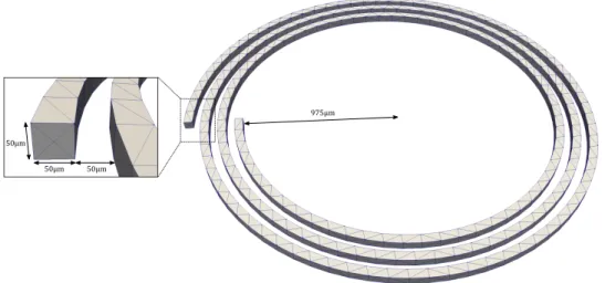
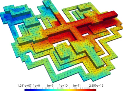
2.7.3 Current density (log-scale) of a superconducting film. A fluxon is trapped in the left hole and zero fluxons in the right hole. Di-mensions: 16 µm×11 µm with thickness of 0.4 µm and London penetration depth of 0.4 µm. Dimensions of holes: 5 µm×2 µm separated by 8 µm. . . 34 2.7.4 The current density (log-scale) of two moats (4µm ×1µm) in a
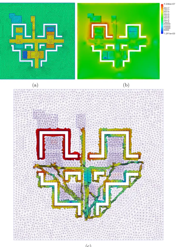
50µm×30µmfilm (thickness 100nmandλ = 966.95nm) calculated using TTH. The two moats are separated by 8µm. . . 34 2.7.5 SFQ pulse splitter example from InductEx website [2]. . . 36 2.7.6 Current density of the SFQ pulse splitter, generated with TTH,
with 1 V applied to portPIb. . . 37
2.7.7 (a) Mesh generated from GDS layout using InductEx. (b) Current distribution of SFQ pulse splitter with a fluxon trapped in moat M1. (c) VL basis functions around moats and between port terminals. 38 2.7.8 circuit schematic of SFQ Splitter with current source (IH1) and
inductor (LH1) representing the fluxon in a moat coupling with the surrounding inductors. . . 39 3.2.1 Triangle T+
m with projected triangles at heights h0m and h1m. . . . 43
3.2.2 RWG basis function at material interface with different conductivities. 44 3.2.3 Closed surface loop basis function. . . 45 3.2.4 Unclosed surface loop basis function with two boundary edges of
lengthsla and lb. . . 46
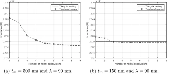
3.4.1 Current density (in log-scale) of a single-layer superconducting film. Each rectangular strips (30 µm×8 µm, thickness = 500 nm, λ = 90 nm) are separated by 4 µm. . . 48 3.4.2 Inductance of single-layer superconducting film as a function of the
number of height subdivisions used for the tetrahedral mesh. . . . 49 3.4.3 Current density of a 50 µm×5 µm microstrip line (thickness =
220 nm and penetration depth = 137 nm) 177.5 nm above ground layer (overhang = 6µm, thickness = 300 nm, and penetration depth = 86 nm). . . 49 3.4.4 Extracted inductance of microstrip line as a function of the number
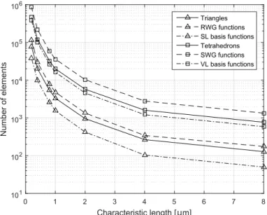
of height subdivisions used for the tetrahedral mesh. . . 50 3.4.5 Number of elements and unknowns as a function of characteristic
length (maximum distance between nodes). . . 50 3.5.1 Hybrid loop basis function. . . 51 3.5.2 Microstrip line (tetrahedrons) above a groundplane (triangles). The
height of the microstrip line is divided into 5 even layers . . . 52 3.5.3 Current density of a 50µm×5µm microstrip line (triangular
mesh-ing) with a via (tetrahedral meshmesh-ing). . . 52 3.5.4 Extracted inductance values for the microstrip line with via. . . . 53
4.1.1 Simple transmission line circuit models. (a) π circuit model. (b) Γ
circuit model. (c) T circuit model. . . 55
4.1.2 The different regimes for transmission line models [3]. (A) Sin-gle lumped inductance, (B) Frequency dependent inductance, (C) Coupled inductance and capacitance. . . 56
4.3.1 Piecewise homogeneous object with Full-SWG functions inside ho-mogeneous regions and Half-SWG basis functions at material in-terfaces. . . 60
4.3.2 Definition of the Half-SWG basis functions. . . 61
4.3.3 VL basis functions, consisting of Half-SWG basis functions, con-structed around an edge; connecting four tetrahedrons with differ-ent dielectric and magnetic constants. . . 65
4.4.1 Convergence rate of GMRES for the copper spiral . . . 68
4.4.2 Convergence rate of GMRES for the permeable cylinder . . . 69
4.5.1 Tetrahedral mesh of the copper spiral with three rotations. . . 70
4.5.2 FastImp model of the copper spiral consisting of rectangular filaments. 70 4.5.3 (a) Extracted impedance of the copper spiral for both MQS and EMQS analysis. (b) Phase of the impedance. . . 71
4.5.4 Scaled version of a two conductor transmission line (σ = 5.8× 10⁷S/m). . . . 72
4.5.5 (a) Extracted impedance of the transmission line for both EMQS and Full-Wave analysis. The two conductors are separated by 0.01 cm. (b) Phase of the impedance. (c) Relative error between EMQS and Full-Wave analysis. . . 73
4.5.6 (a) Extracted impedance of the transmission line for both EMQS and Full-Wave analysis. The two conductors are separated by 1 cm. (b) Phase of the impedance. (c) Relative error between EMQS and Full-Wave analysis. . . 74
4.5.7 Probe-fed patch antenna over a finite ground plane. (a) Dimen-sions of patch antenna. (b) 3D geometry with finite ground plane (165 mm×165 mm) . . . 75
4.5.8 Extracted impedance of patch antenna for different permittivity for the dielectric volume. (a) Real part of impedance. (b) Imaginary part of impedance . . . 75
4.5.9 GDS layout of superconducting transmission line, (a) with vias punching through the ground plane and (b) without vias. (c) 3D model and current distribution of the transmission line with vias generated by TTH (scaled vertically). . . 76
4.5.10(a) Extracted impedance of the superconducting transmission lines, with vias punching through the ground plane and without vias. (b) Phase of the impedance. . . 76
4.6.1 Cross section of permeable cylinder surrounded by a copper coil. . 77
4.6.2 Inductance of permeable cylinder in Fig. 4.6.1. The relative per-meability of the entire cylinder is changed equally, i.e. µr1 =µr2. . 78
4.6.3 Inductance of permeable cylinder in Fig. 4.6.1, calculated with TTH and CST Studio. The relative permeability of the center layer is kept constant atµr2 = 104, whileµr1was adjusted. For comparison purposes, the results are also shown for µr1=µr2. . . 79 4.6.4 Cross section of permeable cylinder surrounded by a copper coil,
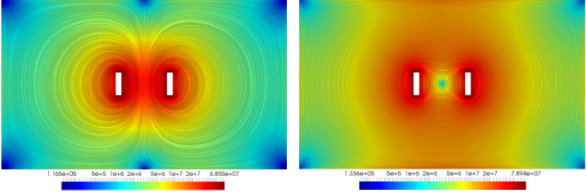
with top and bottom layers connected by a small cylinder. . . 79 4.6.5 Cross section of magnetic current and magnetic field inside the
permeable cylinder of Fig. 4.6.4. (a) The magnetic current den-sity calculated with TTH with the coil excited with 1 V. (b) The magnetic field calculated with CST Studio with 1 A inside the coil. 80 4.6.6 Copper coil above a multilayer permeable substrate. . . 81 4.6.7 Inductance of the coil above the permeable substrate. The relative
permeability of the bottom layer is kept constant atµr2 = 103. . . 81 4.6.8 Cross section of the structure in Fig. 4.6.6. (a) Magnetic current
density calculated with TTH. (b) Magnetic field calculated with CST Studio. (c) Vector field of the magnetic current density calcu-lated with TTH. . . 82 4.6.9 GDS layout of a 100µm×10µm microstrip line with a 32µm×
22µm permeable rectangle sandwich between layers M2 and M0 of the Hypres 4.5 kA/cm2 Nb fabrication process [4]. . . . . 83 4.6.10Electric current density of a superconducting microstrip line above
a ground plane. The relative permeability of layerM1 is µr = 1000. 83
4.6.11Extracted inductance of the microstrip line example for a range of relative permeability values for layer M1 andR2. . . 84 4.6.12Superconducting microstrip line with relative permeability of µr =
1000 for layerM1. (a) Vector field of electric current density,J, and the magnetic current density, M, within the permeable material. (b) Vector field of magnetic current density, M, within permeable material. . . 84 4.6.13GDS layout of a two microstrip lines with a 44µm×38µm
perme-able rectangle sandwich between layers M2 and M0 of the Hypres 4.5 kA/cm2 Nb fabrication process. . . . 85 4.6.14Coupling factor between the two microstrip lines for a range of
relative permeability values. . . 86 4.6.15Microstrip lines above substrate with relative permeability of µr =
1000. (a) Vector field of electric current density, J. (b) Vector field of magnetic current density, M, within permeable material. . . 86 5.2.1 A superconducting washer (size = d×d and constant thickness =
0.5µm) with an applied external magnetic field. . . 92 5.2.2 Computed magnetic flux through a thin superconducting washer.
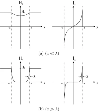
5.2.3 (a) Superconducting slab (thicknesses = 2a and λ = 90 nm) in a z-directed magnetic field, H0. (b) Normalised current density, Jx,
inside superconducting slab, along the y-axis. . . 93 5.3.1 Magnetic field induce by a circulating current in a fictitious coil
with radius rc around a SFQ pulse splitter. . . 95
5.3.2 An equivalent circuit of the fictitious coil,Lc, magnetically coupling
with an inductor,Ls, in the superconducting circuit. . . 95
5.3.3 Current induced in the washer, Im, as a function of the magnetic
field’s amplitude. . . 97 5.3.4 Current induced inside SFQ pulse splitter due to an external
mag-netic field in the z-direction. . . 97 5.3.5 Circuit schematic of the SFQ pulse splitter. Magnetic fields (x-,
y- and z-direction) are modeled as inductors connected to current sources. . . 98 5.3.6 Operating margins of SFQ pulse splitter for magnetic fields in the
x-, y- and z-directions. . . 100 6.5.1 Magnetic field, H, surrounding a superconducting microstrip line.
Streamlines were generated using ParaView [5, 6]. . . 109 6.5.2 Relative error (%) along y-axis for ExaFMM (MAC = 0.3). . . 109 6.5.3 Relative error (%) along y-axis for BiotFMM. . . 110 6.5.4 Calculation time of BiotFMM for different expansion orders (P) vs
direct approach. . . 111 6.5.5 Calculation time of BiotFMM and ExaFMM for a problem
consist-ing of 80,000 observation points. . . 111 6.5.6 Calculation time of BiotFMM and ExaFMM as a function of
List of Tables
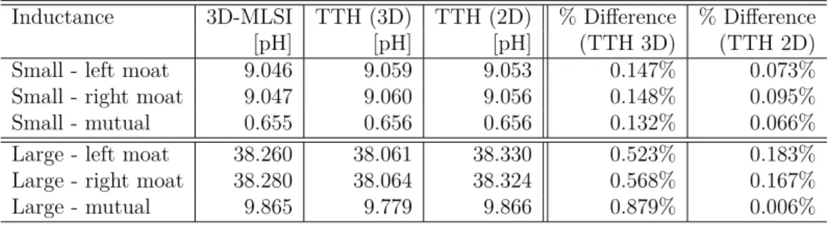
2.7.1 Performance comparison between TTH and FFH. Bench-marked performed on a Intel Core i7-3612QM @2.1 GHz, running Windows 8.1. . . 33 2.7.2 The extracted inductance values of the small structure in Fig. 2.7.3
and the large structure in Fig. 2.7.4 . . . 35 2.7.3 Inductance values of SFQ pulse splitter computed with TTH and
FFH. . . 37 2.7.4 Coupling factors (k) between moats and inductors in SFQ splitter.
Highlighted values indicate the highest coupling factors of each moat. 39 3.4.1 Calculation time of triangular method compared to tetrahedral
method with uniform subdivisions. . . 51 4.6.1 Inductance of the copper coil in Fig. 4.6.1 with µr1 =µr2 = 104. . 78 4.6.2 Inductance and mutual inductance between microstrip lines in Fig. 4.6.13. 86 5.3.1 Coupling factors (k) between fictitious magnetic field coil (Lc =
0.186 pH) and the inductors in Fig. 2.7.5b. The coupling factors are calculated for the magnetic field in the x-, y- and z-direction. 99 6.3.1 Normalised vector spherical harmonics Ψm
n(θ, φ) [7] . . . 105
Chapter 1
Introduction
1.1
Motivation
The improvement of existing silicon-based devices is reaching its limit as the physical structures approach atomic dimensions. Energy efficiency has become the new limiting factor defining processor performance [8]. It is also a dom-inant metric for the next generation of supercomputers [9]. The high energy requirements of complementary metal-oxide-semiconductor (CMOS) devices make it an impractical technology for the next generations of high-end com-puting systems [9].
Alternatively, superconducting electronics outperforms semiconductors with respect to both speed and power dissipation. The use Josephson Junctions devices [10] as ultra-fast switching devices, allows superconducting digital cir-cuits to operate at clock frequencies exceeding 40 GHz and can be boosted to approximately 300 GHz for low critical temperature circuits [11]. Supercon-ducting technologies, such as Adiabatic Quantum Flux Parametron (AQFP) circuits [12, 13], can reduce energy dissipation by several orders when used for parallel pipelining [14], compared to CMOS circuits, and is estimated to be the most energy efficient technology for computations [15].
For superconducting electronics to reach the computational complexities of CMOS processors, very-large-scale integration (VLSI) is required. Before large-scale superconducting integrated circuits can be implemented on physical wafers, several design steps must be followed. One of the design steps is the extraction of circuit parameters from the circuit’s layout. These extracted parameters are then used to verify that the layout corresponds to the circuit schematic.
Inductance plays an important role in superconducting circuit design. Ac-curate inductance extraction is crucial for acAc-curate circuit simulation of single flux quantum (SFQ) circuits. The lack of accurate and fast computational electromagnetics (CEM) solvers for superconducting structures, limits the ca-pabilities for VLSI superconducting circuit design.
1.2
Inductance Extraction
Accurate inductance calculations are crucial when designing superconducting integrated circuits. During the fabrication process, several layers are deposited on top of each other, resulting in irregular topography. Fabrication processes that use planarization methods, such as complemented caldera planarization [16, 17, 18, 19], do not necessary planarize the top layers. The result is complex curvatures that are difficult to model with existing numerical solvers, such as FastHenry [20], that uses rectangular uniaxial filaments. Corners, stacked vias and non-Manhattan structures such as spiral coils are also not easily modelled with rectangular uniaxial filaments.
To overcome this limitation, software, such as InductEx [21, 2], has been developed to extract inductance from complex superconducting circuit lay-outs [22]. The inductance solver, FastHenry, was modified to support super-conductivity [23] and forms the back-end of InductEx. InductEx generates three-dimensional (3D) meshes, consisting of cuboid filaments, as input to FastHenry. Although this approach is efficient for Manhattan layouts, cuboid filaments lack the ability to accurately model uneven multi-directional current flow along curved structures.
FastHenry is a magnetoquasistatic solver and, therefore, lacks the ability to capture distributed capacitance and inductance simultaneously. Modifications have been made to support the full quasistatic Maxwell’s equations [3, 24], but the source code of these versions are not readily available. An impedance ex-traction program, FastImp [25], which uses a surface integral formulation and the precorrected fast Fourier transform (pFFT), is capable of perform full 3-D electromagnetic analysis over a wide-band of frequencies. Unfortunately, the surface integral formulation makes it difficult to accurately analyse the effects of high current density near the surface of a volume. This is especially impor-tant within superconductor, since the London penetration depth determines the distance a magnetic field will penetrate the superconductor [26].
Another significant drawback of superconducting integrated circuits, is the sensitivity to external magnetic fields and fluxons trapped in superconduct-ing films. These trapped fluxons, in the form of Pearl vortices [27], mag-netically couples with surrounding superconducting elements; degrading the circuit’s performance. Previous work [28, 29, 30] has demonstrated tech-niques for analysing trapped fluxons and most require the extraction of in-ductance around holes, formed by trapped fluxons. The software package, 3D-MLSI [31, 32], is capable of extracting self- and mutual-inductance around holes; however, it is limited to two-dimensional superconducting films. The method discussed in [33], can simulate trapped fluxons in Josephson-junction arrays, but this method was only developed for geometries consisting of rect-angular filaments.
Although several tetrahedral modeling methods [34, 35, 36] have already been developed for non-superconducting structures; these methods have not
yet been adapted and implemented for superconducting structures.
1.3
Objectives of dissertation
In this work, we propose a numerical solver, called TetraHenry (TTH), that uses tetrahedral elements to model multi-directional current flow in complex three-dimensional superconducting structures. The numerical solver will be used to perform inductance calculations and flux trapping analysis on large superconducting integrated circuits. The solver, including all the algorithms mentioned in this dissertation, is implemented in C/C++. The accuracy and performance of the numerical engine is evaluated, by comparing simulated results to existing software. The objectives of this dissertation requires several features to be added to the numerical solver:
1. Enabling full-chip simulation and inductance extraction, using hybrid meshes that consisting of both triangular and tetrahedral meshes.
2. Simulating piecewise homogenous dielectric materials, which enables frequency-depended impedance extraction.
3. Simulating piecewise homogenous magnetic materials, used in supercon-ducting memory devices.
4. Adding support for external magnetic fields, to evaluate their effect on the performance of superconducting circuits.
5. Implementing support for hole/moat excitation, which will be used for flux trapping analysis.
6. Implementing numerical techniques, such as iterative solvers with pre-conditioning and the Fast Multipole Method (FMM), to speed up the numerical engine.
In the next Chapter, Chapter 2, the full implementation of the numerical solver, TetraHenry (TTH), is discussed. The full derivation of the current density integral equation (VJIE), with support for superconducting currents, is derived from Maxwell’s equations. A system of linear equations is obtained from the VJIE, using a special Volume Loop (VL) basis function (consisting of SWG functions) and the Method of Moments (MoM). Analytical solutions are derived for the integration over tetrahedrons. The system of linear equations is solved with the GMRES iterative solver and accelerated with preconditioning matrices. The Fast Multipole method is used to accelerate the computation of matrix-vector products. Finally, the performance and accuracy of TTH is compared to FastHenry, for small and large superconducting circuits.
In Chapter 3, the implementation of the two-dimensional triangular method is discussed. An integral equation is derived for the two-dimensional sheet current model. The Surface Loop (SL) basis function, consisting of RWG functions, is introduced. Analytical solutions are derived for the integration over triangles. The advantages of triangular meshing for large superconducting circuit layouts, consisting of thin superconducting films, are demonstrated. The the performance and accuracy of the triangular method is compared to the tetrahedral method.
The full derivation of the integral equations for electric and magnetic cur-rents, inside inhomogeneous dielectric and magnetic materials, is discussed in Chapter 4. Special Half-SWG basis function are used to account for electric and magnetic charge accumulation on material interfaces. The interaction between magnetic and electric currents is accelerated, using the Biot-Savart FMM (BiotFMM) derived in Chapter 6. Preconditioners are developed to accelerate the iterative solver. The impedance of several test structures are extracted, using both electro-magneto-quasi-static (EMQS) analysis and Full-Wave analysis. The effects of magnetic materials on non- and superconducting structures are evaluated. The accuracy of TTH is compared to existing soft-ware packages, such as FastImp and CST Studio.
The implementation of uniform external magnetic fields is discussed in Chapter 5. The magnetic vector potential of a predefined uniform magnetic field, with x-, y- and z-components, is derived and implemented into the ex-isting VJIE formulation. An equivalent circuit model for the magnetic field is derived, which can be used to evaluated the effects of magnetic fields on the operating margins of SFQ circuits.
The full derivation of the FMM algorithm for the Biot-Savart law, re-ferred to as BiotFMM, is discussed in Chapter 6. The BiotFMM algorithm replaces the direct multiplication of Biot-Savart law, which is used to calcu-late the interaction between electric and magnetic currents, see Chapter 4. The BiotFMM algorithm can also be implemented directly into the exist-ing FastCap or FastHenry code. Finally, the accuracy and performance of BiotFMM are compared to the existing library, ExaFMM.
Appendix A contains the published article, “Flux Trapping Analysis in Superconducting Circuits” [37]. VL basis functions are used to specify the number of fluxons inside each hole or moat. The inductance of holes and the mutual-inductance between holes are extracted, including the energy of trapped fluxons in the presence of external magnetic fields. These extracted values are then used to calculate the probability of flux trapping.
Appendix B contains the published article,“Fast Multicore FastHenry and a Tetrahedral Modeling Method for Inductance Extraction of Complex 3D Ge-ometries” [38]. In this article, the algorithmic improvements made to the numerical solver, FastHenry, are discussed.
Lastly, a user’s manual for TTH is provided in Appendix C. All the input commands and file requirements are specified, including the geometry files
Chapter 2
3D Tetrahedral Modelling
Method
2.1
Introduction
In this chapter, a detailed description of the newly developed numerical solver, called TetraHenry (TTH), is provided. TTH uses tetrahedral volume elements to discretize complex geometries and is capable of modeling multidimensional current flow in superconducting structures. The volume electric current in-tegral equation (VJIE), used in [39, 40, 41, 42, 36], was chosen as the most suitable method for modeling superconducting currents. The VJIE formula-tion is similar to the VIE used in FastHenry and requires less iteraformula-tions when using an iterative method [40]. It is also more stable for extremely anisotropic materials [41] compared to the electric flux density formulation (VDIE) [34].
The VJIE formulation is derived for superconducting structures, starting with the magneto-quasistatic (MQS) Maxwell’s equations and assuming sinu-soidal steady-state. Volume Loop (VL) basis functions [35], a combination of Schaubert-Wilton-Glisson (SWG) functions [34], are used to discretize the VJIE. The Method of Moment (MoM) [43] is used to construct a linear sys-tem of equations from the VJIE, which is solved using the GMRES iterative method [44]. The matrix-vector product in the GMRES is accelerated using the Fast Multipole Method (FMM) [45]. Meshing is done by a third party finite element mesh generator, i.e. Gmsh [46, 47]. Algorithmic improvements and parallelization methods developed in [38], see Appendix B, have also been modified and implemented in TTH. The entire numerical engine, including the algorithms mentioned in this Chapter, was fully implemented in C/C++.
2.2
Background Formulation
The aim is to extract the inductance between several terminals by computing the complex frequency-dependent impedance matrix of a multi-terminal
tem, similar to the method used in FastHenry. The problem is solved under the magnetoquasistatic (MQS) approximation, described in [20]. This will re-quire solving the following linear equation at a given excitation frequency ω:
Zm(ω)Im(ω) =Vm(ω) (2.2.1)
where Im(ω), Vm(ω) ∈ Cm are vectors containing the current and voltage
phasors at the terminals, respectively [20]. The complex impedance matrix
Zm ∈Cm×m for the two conductor example, shown in Fig. 2.2.1, will be of the
form: Zm(ω) = Rm(ω) +jωLm(ω) = " R11(ω) +jωL11 R12(ω) +jωL12 R21(ω) +jωL21 R22(ω) +jωL22 # (2.2.2)
where Rm, Lm ∈ Cm are the resistance and inductance matrix, respectively.
The valueL11is the self-inductance of conductor 1 andL12=L21is the mutual inductance between the two conductors. If the vectors Im and Vm are known,
the i column of Zm can be calculated by setting the value at index i in Im
equal to 1 and the rest to zero.
Figure 2.2.1: Two conductors with sinusoidal excitation voltages at given fre-quency.
2.3
Derivation of Volume Integral Equation
Several volume integral equation (VIE) formulations exist for inhomogeneous dielectric problems; either based on electric flux density [34, 48], electric field intensity [48, 49] or current density [36, 40, 41]. In order to calculate the inductance between two terminals, both the current and voltage at each ter-minal is required. The VIE formulation described in [36] is ideal, since it the uses the volume electric current integral equation (VJIE) and is similar to the method used by FastHenry. The VJIE require less iteration when using an iterative method [40] and is more stable [41] compared to the electric flux density formulation (VDIE) [34].
The finite element method (FEM) is used to model the non-uniform cur-rent density within the superconducting volumes. To implement the FEM method, the current carrying volumes are discretized using tetrahedral ele-ments; whereas the free-space regions between structures are not discretized. The material properties of each individual tetrahedral element can be speci-fied, allowing for variation in material properties, which is ideal for piecewise homogeneous bodies.
In addition to the FEM method, the Method of Moments (MoM) [43] is used to solve a volume integral equation (VIE), which will be derived in this Chapter. The Method of Moment is a powerful numerical technique for solving open-region electromagnetic problems [50]. The MoM transforms a boundary-value problem into a matrix equation and does not required the free-space regions to be discretized [50]. This makes the MoM ideal for simulating large superconducting integrated circuits, since the dielectric materials surrounding the superconductors do not require meshing. This is a valid assumption, if the displacement currents, jωE, are to be assumed negligible compared to the currents within the superconductors. However, this assumption is not valid at high frequencies, which requires discretizing the dielectric regions, as will be discussed in Chapter 4. In this Chapter, it is assumed that frequency is relatively low and that the displacement current is negligible.
Starting with Maxwell’s equations and assuming sinusoidal steady-state,
∇ ×E=−jωµH, (2.3.1)
∇ ×H=jωE+J, (2.3.2)
∇ ·(E) = ρ, (2.3.3)
∇ ·(µH) = 0, (2.3.4)
the VJIE formulation can be derived. The displacement current is assumed negligible, i.e. magnetoquasistatic (MQS) approximation, since the conduc-tivity is large within the conductors. From Ohm’s law the volume electric current, J(r), within the conductor can be expressed as:
J(r) =σ(r)E(r). (2.3.5)
where σ(r) is the conductivity. Under the quasistatic assumption, the diver-gence of the current becomes:
∇ ·J(r) = 0, (2.3.6)
and for ideal current sources:
∇ ·J(r) =Im(r). (2.3.7)
From Maxwell’s equations it can be shown that:
where A(r) is the magnetic vector potential: A(r) = µ 4π Z V0 J(r0) |r−r0| dv. (2.3.9)
From (2.3.5), (2.3.8) and (2.3.9), the following integral equation can be derived:
J(r) σ(r)+ jωµ 4π Z V0 J(r0) |r−r0| dv 0 =−∇φ(r), (2.3.10)
whereφ(r) is the scalar potential. The conductivity,σ(r), can vary within the conductors and the permeability is considered constant: µ=µ0.
2.3.1
Superconductivity
For a material in superconducting state, the total current consists of a normal-and super component:
J =Jn+Js, (2.3.11)
where Jn is the normal current, i.e. the flow of normal electrons, and Js is
the superconducting current, i.e. the flow of Cooper-pairs [26]. The relation between the total current and the electric field resembles Ohm’s law [26]. This relation can be expressed in the sinusoidal steady state as:
J =Jn+Js= σ˜0+ 1
jωµλ2 !
E, (2.3.12)
whereλ=λ(T) is the temperature depended London penetration depth of the superconductor with critical temperature TC:
λL(T) = λL(0) r 1− T TC 4 , (2.3.13)
and ˜σ0 = ˜σ0(T) is the temperature-dependent conductivity of the normal channel [26]. The London penetration depth determines the depth a magnetic field will penetrate a superconducting volume from the surface. Section 2.6.1 provides a detailed description of the penetration depth and how meshing is adapted to account for this penetrating field. Support for superconductivity can now be added to (2.3.10) by substituting σ(r) with k(r):
J(r) k(r) + jωµ 4π Z V0 J(r0) |r−r0| dv 0 =−∇ φ(r), (2.3.14) where k(r) = ˜σ0(r) + 1 jωµλ(r)2. (2.3.15)
2.3.2
Discretization
A special basis function was developed for tetrahedral meshes, known as the SWG function [34], which can be used to discretize the VIE. The SWG func-tion can also modified into Half- and Full-SWG funcfunc-tions for piecewise homo-geneous dielectrics [36], as will be discussed in Chapter 4. It was shown in [36] that the Full-SWG and Half-SWG basis functions (JSWG) are as accurate as the DSWG basis method used in [34].
Figure 2.3.1 shows an arbitrary body with piecewise constant electrical pa-rameters, discretized using Full-SWG functions. Figure 2.3.2 and 2.3.3 show the definition of the Full-SWG basis function, with constant electrical param-eters in each tetrahedron. The two tetrahedrons, T+
n and T
−
n, are associated
with thenth face of the discretized volume. The vectors,ρ+
n andρ
−
n, represent
the position vectors in Tn+ and Tn−, respectively. In tetrahedron Tn+, the po-sition vector ρ+
n is defined with respect to the free vertex and in T
−
n towards
the free vertex [34], see Fig.2.3.3. The signs of the two tetrahedrons depend on the choice of the direction of current flow through the nth face.
Figure 2.3.1: Full-SWG basis functions in arbitrary body with piecewise con-stant electrical parameters.
Figure 2.3.2: Full-SWG basis function at material interface (σ1 6=σ2).
Since J(r) is not continuous across material interfaces of inhomogeneous dielectric bodies, surface charges will accumulate at material interfaces. For piecewise homogeneous dielectric objects, the Half-SWG function should be
Figure 2.3.3: Full-SWG basis function.
used at material interfaces, as discussed in Chapter 4. To simplify the prob-lem, the entire volume is first assumed to be a homogeneous dielectric body, preventing surface charges accumulation. The Full-SWG function can then be used within the entire volume:
fn(r) = 1 3|v+n|ρ + n(r), if r∈Tn+ 1 3|v−n|ρ − n(r), if r∈T − n 0, otherwise , (2.3.16)
where |vn±| represents the volume of tetrahedron Tn±. This function differs from the basis functions used in [34] and [36], which uses the area of the face to normalize fn(r). Using Full-SWG functions, the volume electric current
density, J(r), can be expanded as follow:
J(r) =
N
X
n=1
infn(r), (2.3.17)
where N is the number of faces that make up the entire volume and in is the
branch current through the nth face. The total volume electric current within the tetrahedron,Tq, can be calculated by summing the four linear independent
basis functions, associated with each face of the tetrahedron [34],
Jq(r) =
4 X
n=1
infn(r), r∈Tq. (2.3.18)
Following the Method of Moments [50], the VIE can be solved by defining the equation:
L(J(r)) =v, (2.3.19)
where L denotes the linear operator, which will be left-hand side of (2.3.14). The vector function v is known, whereasJ(r) needs to be solved. Next, a set of weighting functions, w1(r),w2(r), ..,wm(r), in the range of L are defined.
The weighting functions, wm(r), are defined as Full-SWG functions, as given
in (2.3.16). To obtain a system of linear equations, the inner products between (2.3.14) and the weighting functions are used:
N
X
n=1
where <·>denotes the inner product of two vector functions [50]. Equation can now be written in matrix format:
ZIbranch =Vbranch, (2.3.21) where Z = <w1,L(f1)> . . . <w1,L(fn)> . . . <w1,L(fN)> <w2,L(f1)> . . . <w2,L(fn)> . . . <w2,L(fN)> .. . . .. ... . .. ... <wm,L(f1)> . . . <wm,L(fn)> . . . <wm,L(fN)> .. . . .. ... . .. ... <wN,L(f1)> . . . <wN,L(fn)> . . . <wN,L(fN)> , (2.3.22) and Ibranch = i1 .. . in .. . iN , Vbranch = <w1,v1 > <w2,v2 > .. . <wm,vm > .. . <wN,vN > , (2.3.23)
From (2.3.22) the matrix Z can be decomposed into its real and imaginary components:
Z =R+jωL, (2.3.24)
where R and L are respectively the resistance and inductance matrices. The entries of the resistance matrix are computed as follow:
Rm,n =
Z
vm 1
k(r)wm(r)·fn(r)dv, (2.3.25)
and the entries of the inductance matrix:
Lm,n = µ 4π Z vm Z vn wm(r)·fn(r0) |r−r0| dv 0 dv. (2.3.26)
The values Rm,n and Lm,n correspond to the Full-SWG basis functions m and
n. The volumesvm and vn represent the volumes of the SWG-basis functions,
which are a combination of (T+
m+T
−
m) and (Tn++T
−
n), respectively. The voltage
over each face is stored in the vector, Vbranch, and can be computed as follow:
(Vbranch)m =<wm,vm >=−
Z
vm
wm(r)· ∇φ(r)dv, (2.3.27)
given the vector function, vm =∇φ(r), over face m.
Using the basis function defined in (2.3.16), it is difficult to apply boundary conditions to (2.3.27), e.g. excitation voltage between two terminals. Using the volume loop (VL) basis function, discussed in Section 2.3.3, it is possible to restrict current flow to a solenoidal subspace in which Kirchhoff’s voltage law (KVL) is enforced.
2.3.3
Volume loop basis function
The divergence of the electric flux within homogeneous dielectric bodies, in-cluding superconducting volumes, is zero. This poses a problem, since the divergence of the SWG basis function is non-zero [34],
∇ ·fn(r) 1 3|vn+|, if r∈T + n 1 3|vn−|, if r∈T − n 0, otherwise . (2.3.28)
From the continuity equation,
∇ ·J(r) =jωρ(r), (2.3.29)
it is clear that the charge density is constant within each tetrahedron [35]. Several schemes have been developed to ensure divergence free currents within tetrahedral meshes, such as the basis reduction scheme [51], edge-based solenoidal basis functions [52, 53, 35], and volume loop (VL) basis set consisting of SWG functions [42].
The basis reduction scheme enforces divergence free current within each tetrahedron. The sum of the 4 basis functions associated with each face of the tetrahedron must equal zero [35]. Although the basis reduction scheme reduces the number of unknowns, it results in a matrix equation with a large condition number, making it difficult to solve with an iterative method [35].
The volume loop (VL) basis is a solenoidal basis function that restricts current flow to a solenoidal subspace and enforces Kirchhoff’s voltage law. This approach is similar to the methods used in [20] and [54]. VL basis functions are constructed around the edges of a tetrahedral mesh, which ensures divergence free current within a homogeneous dielectric body. Figure 2.3.4 and 2.3.5 illustrate the closed and unclosed volume loop (VL) basis functions around an edge, respectively. The VL basis function around edge m can be defined as a combination of SWG functions, fn(r), om(r) = N X n=1 Mm,nfn(r), (2.3.30)
whereMm,n =±1, depending on the direction offn(r) within loopm[42]. The
value of Mm,n is zero, if fn(r) does not form part of loop m. The value N is
the total number faces inside the tetrahedral mesh.
The volume electric current density, J(r), can now be expanded in terms of VL basis functions: J(r) = M X m=1 imom(r) = M X m=1 im ( N X n=1 Mm,nfn(r) ) , (2.3.31)
Figure 2.3.4: Close volume loop basis function.
Figure 2.3.5: Unclosed volume loop basis function.
where im is defined as the mesh current circulating around loop m, which is a
combination of several branch currents, in:
im = N
X
n=1
Mm,nin. (2.3.32)
The mesh currents are stored within the vector, Imesh, and can be computed
from the current vector, Ibranch, defined in (2.3.23):
Imesh =M Ibranch. (2.3.33)
The entries of matrixM at indexes (m, n) are equal to the values,Mm,n, given
in 2.3.32. Each row of M represents a single VL basis function. The column index of M determines which currents from Ibranch, i.e. SWG functions fn(r),
form part of the VL basis function. The system of equations given in (2.3.24) can now be transformed as follows:
M ZIbranch =M Vbranch, (2.3.34)
and replacing Ibranch with Imesh,
M ZMTImesh =Vmesh. (2.3.35)
The vector, Vmesh, contains the voltages across each VL basis function and is
defined as,
It is shown in [42] that the values of the vector Vmesh will become zero for
closed VL basis functions and will be equal to the voltage difference across the ends of unclosed VL basis functions:
(Vmesh)m =
0, for closed loop m
φ(ξ)|ξ∈Aa −φ(ξ)|ξ∈Ab, for unclosed loopm
. (2.3.37)
The functions φ(ξ)|ξ∈Aa and φ(ξ)|ξ∈Ab represent the constant voltage potential across the two faces at the ends of an unclosed loop, with area Aa and Ab,
respectively.
Figure 2.3.5 illustrates the setup of the VL basis functions within a rectan-gular filament, with a voltage source connected to two terminals. The points represent edges viewed from above and the circles represent closed VL basis functions. Since displacement current is assumed negligible, current will not flow across the boundary and SWG basis functions are not required for bound-ary faces. However, the faces connected to the terminals require SWG basis functions, since current can exit these faces. Closed VL basis functions around the terminal edges ensure that the terminal faces are shorted electrically. An unclosed VL basis function is defined between the two terminals and represents the voltage difference between the two terminals, as shown in (2.3.37).
Figure 2.3.6: Top view of tetrahedral mesh of rectangular filament with two terminals.
2.3.4
Fundamental Set of Basis Functions
If VL basis functions are expanded to each possible edge, the basis functions will no longer be independent, resulting in a null space in the matrix equation.
It is shown [35] that this null space is not detrimental when using iterative solvers. However, this is not the case when preconditioners are used to im-prove the convergence rate of the iterative solver, which will be discussed in Section 2.5.2. A set of independent (fundamental) VL basis functions can be obtained, using the generating (spanning) tree scheme described in [35]. The basis reduction scheme [35] can also be used to reduce the number of loops, but this approach results in a poorly-conditioned matrix, due to many overlaps between loops.
Using the generating tree scheme, an undirected graph is constructed from the geometrical (tetrahedral) mesh. The tetrahedrons and faces represent the nodes and edges of the undirected graph, respectively. If displacement current is taken into account, as discussed in Chapter 4, an additional node must be used for the outer space. A spanning tree is then constructed from this undi-rected graph and the remaining edges, i.e. edges that do not form part of the spanning tree, are used to obtain a set of independent VL basis functions. This approach (hereafter referred to as the tetrahedral tree scheme) is equivalent to finding a set of fundamental circuits in a graph [55].
The nodes and edges of the tetrahedral mesh can also be used to construct an undirected graph [35]. An independent VL basis set can be obtained by constructing VL basis functions around the edges that do not form part of the spanning tree. This method (hereafter referred to as the edge tree scheme) can be easily implemented, but it is limited to simply connected regions that do not contain any holes [35]. If a structure contains a hole, an addition VL basis function must be constructed around the hole, resulting in a null space in the matrix equation. As mentioned before, the null space in the matrix equation is not detrimental when using iterative solvers. However, it can limit the ability to perform LU decomposition, which is necessary for preconditioning.
One advantage of the tetrahedral tree scheme, is that multiple VL basis functions are automatically constructed around holes. This can also be con-sidered a disadvantage, because it is difficult to identify the VL basis functions surrounding each hole. To perform flux trapping analysis, see Appendix A, the voltage of these VL basis functions must be specified in order to induce current around specific holes. Another disadvantage of the tetrahedral tree scheme is the large VL basis functions, created by the spanning tree, which increase the number of non-zero values in the sparse matrix, M ZMT.
The edge tree scheme reduces the number of non-zero values in the sparse matrix, M ZMT, since the size of each VL basis function depends only on the
number of faces connected to each edge. The disadvantage of this approach is that the VL basis functions must be specified manually by the user for each hole, which can also be detrimental to LU decomposition. Since the VL basis functions around each hole are manually specified, it reduces the complexity of inducing current around holes and makes it ideal for flux trapping analysis. The tetrahedral tree scheme is suitable for most problems described in this dissertation; whereas theedge tree scheme will be used for hole excitations and
flux trapping analysis.
2.3.5
Port Excitations
Ports are defined between two terminals, one positive and the other negative, as shown in Fig. 2.3.8. To extract the current through the ports, an excitation voltage must be applied to one of the ports. Each port has to be excited independently, while the remaining ports are electrically shorted. This step has to be repeated for each port. If N ports are defined, N2 currents will be extracted. The excitation voltages are specified in the vector Vmesh, i.e.
the right-hand side of (2.3.35). The mesh currents, Imesh in (2.3.35), have be
solved for each excited port. Once all the mesh currents are obtained, the inductance matrix can be calculated, as discussed in Section 2.2.
First, closed VL basis functions have to be constructed around internal and terminal edges, as discussed in Section 2.3.3. The mesh voltages, corre-sponding to the closed VL basis functions, have to be set equal to zero in the vector Vmesh. If a closed VL basis functions is constructed around a hole, the
corresponding voltage in vectorVmesh will depend on the flux through the hole,
see Appendix A.
To construct unclosed VL basis functions between the terminals of each port, an undirected graph is constructed from the topological structure of the mesh. Figure 2.3.7 illustrates the constructed graph of two conductors with two excitation ports. The centroid of each tetrahedron represents a node in the graph, while the connections between a tetrahedron and its neighbouring tetrahedrons represent edges in the graph. A pseudo tetrahedron is used to represent each port, i.e. a connection between two terminals.
This graph can now be used to determine the shortest path (VL basis function) between two terminals. The shortest path between two nodes in a graph can be obtained using Dijkstra’s algorithm [56]. When determining the shortest path between two terminals, all the other ports are electrically shorted, using a pseudotetrahedron. Thepseudo tetrahedrons add additional nodes to the graph; forming connections between positive and negative terminals.
Each port must have a unique path that connects its two terminals. If two identical paths are created, the linear system in (2.3.35) will be ranked deficient and unsolvable. The two port example in Fig. 2.3.7 will result in two identical paths, but their direction will be reversed. The magnitude of the current through these two ports will be identical, but in the opposite direction. To overcome this, paths are compared with each other and duplicate paths are removed from the matrix M, given in (2.3.35).
When a path (VL basis function) crosses several ports, those ports must be taken into account when specifying the mesh voltages in Vmesh. Figure 2.3.8
illustrates three ports with two paths. Path 1 is the unclosed VL basis func-tions of port A, while path 2 is the unclosed VL basis function of both port B and C. When port A is excited, the terminals of both port B and C are electrically shorted and path 2 will become a closed VL basis function.
Figure 2.3.8: Three port example with paths through multiple ports.
It is important to note that when either port B or C is excited, path 1 will remain an unclosed VL basis function. Therefore, the voltage difference over the unclosed VL basis function (path 1) will not be zero, since it is crossing an excited port (either port B or C). If port B or C is excited, the voltage of the unclosed VL basis function (path 1) will be either ±(Vmesh)B or ±(Vmesh)C,
depending on the direction of path 1 and the polarity of the port B and C.
2.4
Resistance and Inductance Matrices
To obtain the currents inside each VL basis function, the system of linear equations in (2.3.35) has to be solved. Before this can be accomplished, the entries of the resistance and inductance matrices, given in (2.3.25) and (2.3.26),
have to be calculated. Luckily, existing numerical methods can be used to evaluate single integrals over tetrahedrons.
In this section, it will be shown that the resistance matrix, R, is mostly sparse, containing only a few non-zero values; whereas the inductance matrix,
L, is dense. An analytical solution can be derived for each entry of the re-sistance matrix, which can be computed and stored directly. However, the inductance matrix cannot be computed and stored directly, due to the size of the matrix. To compute of the inductance matrix, the electrostatic anal-ogy, described in [20], is used and accelerated with the Fast Multipole Method (FMM) [45].
2.4.1
Resistance Matrix
Since each Full-SWG basis function stretches over two tetrahedrons, T+
m and
Tm−, each entry of the resistance matrix, given in (2.3.25), can be separated into two components:
R =R++R−. (2.4.1)
The entries of matrix R+, corresponding to the positive tetrahedron, T+
m, can
now be written as,
(R+)m,n = 1 k+ m Z Tm+ wm(r)·fn(r)dv, (2.4.2)
and the entries of matrixR−, corresponding to the negative tetrahedron,Tm−,
(R−)m,n = 1 k− m Z Tm− wm(r)·fn(r)dv. (2.4.3)
The conductivity within each tetrahedron is assumed constant:
km+ =k(r), r∈Tm+, (2.4.4)
km− =k(r), r∈Tm−. (2.4.5)
Substituting (2.3.16) into (2.4.2), the entries of the resistance matrix,R+, can be computed as follow: (R+)m,n = 1 k+m R Tm+ 1 3|vm+|ρ + m(r) · 1 3|v+n|ρ + n(r) dv, if T+ m =Tn+ 1 k+m R Tm+ 1 3|vm+|ρ + m(r) · 1 3|v−n|ρ − n(r) dv, if T+ m =T − n 0, if T+ m 6=T ± n . (2.4.6)
Although not discussed here, the entries of matrix R− can be computed simi-larly.
From (2.4.6) it is evident that the majority of the values in matrixR+ will be zero, except when T+
m = Tn±. For rest of this section, it is assumed that
Tm+ =Tn+ and v+m =v+n, unless stated otherwise. The position vectors, ρ+m(r) and ρ+
n(r), are defined with respect to their free vertices, see Fig. 2.3.3. If r+m
and r+
n are respectively the free vertices of ρ+m(r) and ρ+n(r), (2.4.6) can be
written as: (R+)m,n = 1 9km|vm+||vn+| Z Tm+ (r−r+m)·(r−r+n)dv = 1 9km|vm+||vn+| Z Tm+ x−x+ m y−y+ m z−zm+ · x−x+ n y−y+ n z−z+n dv = (R+x)m,n+ (Ry+)m,n + (Rz+)m,n, (2.4.7) where (R+
x)m,n represents the contributions of the x-components:
(Rx+)m,n = 1 9km|vm+||vn+| Z Tm+ (x−x+m)·(x−x+n)dv = 1 9km|vm+||vn+| Z Tm+ (x2+x+mx+xn+x+x+mx+n)dv. (2.4.8)
Taking the origin of the coordinates at the centroid of T+
m and using the
integration formula for a tetrahedron [57], the analytical solution for (2.4.8) is as follow: (Rx+)m,n = 1 9km|vm+||vn+| 1 20(x 2 1+x 2 2+x 2 3+x 2 4) +x + mx + n , (2.4.9)
where x1, ..., x4 are the 4 vertices (x-coordinates) of tetrahedron Tm+. It is
important to note that origin of the coordinates (x1, ..., x4, x+m and x+n) are
at the centroid of T+
m. The analytical solution of (Ry+)m,n and (R+z)m,n can
be obtained from (2.4.9), by replacing the x-coordinates with the y- and z -coordinates, respectively. Equation (2.4.9) is an exact solution and can be easily implemented in code.
2.4.2
Electrostatic Analogy
Computing the entries of the inductance matrix, given in (2.3.26), is difficult since it requires the evaluation of a double integral over two tetrahedrons. An analytical solution for (2.3.26) has not yet been derived. However, analytical expressions have been derived for potential integrals of linear source distribu-tions on polyhedral domains [1]. Also, numerical quadrature schemes [58] are available to evaluate the outer integral, while using the analytical expressions for the inner integral.
As demonstrated in [20], the FMM can be used to evaluate the matrix-vector product, ZIbranch, without explicitly forming Z. The matrix-vector
product, ZIbranch, can be separated into a real and imaginary part:
ZIbranch =RIbranch+jωLIbranch. (2.4.10)
The evaluation ofRIbranchis not computationally expensive, sinceRis a sparse
matrix, as shown in Section 2.4.1. However, L is a dense matrix and LIbranch
is computationally expensive to compute directly.
Using the electrostatic analogy, it is possible to compute LIbranch by
eval-uating the electrostatic potential, produced by surrounding charges, at each tetrahedron [20]. Each entry of the matrix-vector product, LIbranch, can be
evaluated as follows: (LIbranch)m = N X n=1 µ 4π Z Tm± Z Tn± wm(r)·fn(r0) |r−r0| dv 0 dv, ! in, (2.4.11)
where in is the branch current through face n, i.e. the coefficient in (2.3.17).
Note that the integration in (2.4.11) is performed over the tetrahedrons Tm±
and Tm±, and not over the volumes vm and vn, as given in (2.3.26). Equation
(2.4.11) can also be written in terms of the magnetic vector potential, A(r), (LIbranch)m = Z Tm± wm(r)·A(r)dv (2.4.12) where A(r) = µ 4π N X n=1 Z Tn± fn(r0) |r−r0| dv 0 ! in = µ 4π N X n=1 Z Tn± ρ±n |r−r0| dv 0 ! in 3|v± n| . (2.4.13)
This decomposition shows that (LIbranch)m can be evaluated by integrating
the magnetic vector potential, A(r), over each tetrahedron. The vector po-tential can be decomposed into its x-,y-, andz-components. Each component can be considered a scalar electrostatic potential generated by a collection of charges [20]: ψp(r) = µ 4π N X n=1 Z Tn± (ρ±n)p |r−r0| dv 0 ! in 3|v± n| , (2.4.14)
wherep∈ {1,2,3}and the scalar potential,ψp(r), denotes the pth component
ofA(r). The product (in/3|v±n|) (ρ
±
n)p can be interpreted as the charge density
within Tn±. If it is assumed that A(r) varies slowly across Tn±, (2.4.14) can be approximated by taking the value at the centroid of the tetrahedron [34]:
ψp(r)≈ µ 4π N X n=1 Z Tn± 1 |r−r0| dv 0 ! in 3|v± n| (ρcn±)p, (2.4.15)
![Figure 2.4.1: Geometrical quantities associated with the ith edge on the j th face of the tetrahedron [1].](https://thumb-us.123doks.com/thumbv2/123dok_us/10142175.2915520/37.893.282.608.227.586/figure-geometrical-quantities-associated-ith-edge-face-tetrahedron.webp)
![Figure 4.1.2: The different regimes for transmission line models [3]. (A) Sin- Sin-gle lumped inductance, (B) Frequency dependent inductance, (C) Coupled inductance and capacitance.](https://thumb-us.123doks.com/thumbv2/123dok_us/10142175.2915520/70.893.263.632.119.516/different-transmission-inductance-frequency-dependent-inductance-inductance-capacitance.webp)