Int. J. Adv. Res. Sci. Technol. Volum e 3, Issue 4, 2014, pp.208-212
International Journal of Advanced Research in
Science and Technology
journal homepage: w w w .ijarst.com
IS S N 2319 – 1783 (Print)
IS S N 2320 – 1126 (Online)
Design of 2-Dimensional Multiplier Using Area efficient and Power Optimization
Technique
Kesanak urthi Rajasek har*and J. Kiran Chandrasek har
Department of ECE, Vizag Institute of Technology, Visakhapatnam, Andhra Pradesh, India.
*Corresponding Author Email: [email protected]
A R T I C L E I N F O A B S T R A C T
Article history:
Received Accepted Available online
20 Nov. 2014 19 Dec. 2014 25 Dec. 2014
Based on the simplification of the addition operations in a low-power bypassing-based multiplier, a low-cost low-power bypassing-based multiplier is proposed. Row-bypassing multiplier, column-bypassing multiplier, 2-Dimensional bypassing multiplier and braun multipliers are implemented in CMOS and GDI technique. By optimizing the transistor size in each stage the power and area are minimized. The results of post -layout simulation compared to similar reported ones illustrate significant improvement. Simulation results show great improvement in terms of Power. The experimental results show that our proposed low-cost low power multiplier saves hardware cost and reduces the power dissipation.
© 2014 International Journal of Advanced Research in Science and Technology (IJARST).
All rights reserved.
Keywords:
Row bypassing multiplier, Column bypassing multiplier, 2-Dimensional bypassing multiplier,
GDI, and power dissipation.
Introduction:
As we get closer to the limits of scaling in complementary metal oxide semiconductor (CMOS) circuits, speed issues are becoming more and more important. In recent years, the impact of pervasive computing and the internet have accelerated this trend. The applications for these domains are typically run on battery-powered embedded systems.
The resultant constraints on the speed require design for speed as well as design for performance at all layers of system design. Thus increasing speed is a key design goal for portable computing and communication devices that employ increasingly sophisticated signal processing techniques.
However, there is a fundamental trade-off between efficiency and flexibility, and as a result, programmable designs incur significant performance and speed compared to application specific solutions. Consequently various digital signal processing chips are now designed with high speed performance. Signal processing applications typically exhibit high degrees of parallelism and are dominated by a few regular kernels of computation such as multiplication, that are responsible for a large fraction of execution time and energy. In such systems, multiplier is a fundamental arithmetic unit.
Introduction:
Diff types of multipliers:
This chapter reveals the design considerations of High Speed parallel multiplier. The design of efficient logic circuits is a fundamental problem in the design of high performance processors. The design of fast parallel multipliers is important, since multiplication is a commonly used and expensive operation.
This is particularly critical for specialized chips that support multiplication intensive operations, such as digital signal processing and graphics. It can also be useful for pipelined CPUs, where faster multiplier components and multipliers can result in smaller clock cycles and/or shorter pipelines.
The various multipliers are:
1. 4x4 Braun multiplier
2. 4x4 Row bypassing multiplier 3. 4x4 Column bypassing multiplier 4. 4x4 2-Dimensional bypassing multiplier
4x4Braun multiplier:
Int. J. Adv. Res. Sci. Technol. Volum e 3, Issue 4, 2014, pp.208-212 Another high speed designs disable the operation in
some rows, designed a technique that reduces the switching to fairly good extent.
Fig.1: Schematic diagram of Braun multiplier
4x4 Row bypassing multiplier:
The Row bypassing multiplier reduces the switching activity by bypassing the row in which the multiplicand bit is zero. That means in the multiplier if a bit is zero then that row of adders will get disabled. For example consider the multiplication of 1011 x 1010. Here the multiplier consists of zero in first and third positions. During multiplication the first and third row of adders get disabled and previous sum is taken as the present sum.
Fig.2: Schematic diagram of Row by passing multiplier
Here a special circuitry called adding cell is used instead of full adders. It consists of three state gates, full adder and multiplexers. The inputs i.e. the partial products to be summed up are given to the full adder through three state gates. The enable input to the three state gates and multiplexers is the corresponding multiplier bit. If this bit is zero then the three state gates goes into high impedance state and thus inputs are not given to the full adder. The previous sum is only taken as the present sum. If this bit is one then the three state gates gets enabled and the inputs are given to the full adder. Thus the sum is generated and this is taken as the present sum.
Fig. 3: Internal structure of adding cell
In this adding cell the three state gate will enabled only when Xj =1 and then the adder will get input. If Xj =0 then the previous sum and carry only will be taken as the present sum and carry. Thus row bypassing can be done by this adding cell (AC).
In this way the switching activity can be reduced if the multiplicand bit is zero. Thus switching activity in row bypassing multiplier is less than that of Braun multiplier. But the only disadvantage of this row bypassing multiplier is that it needs extra circuitry than Braun multiplier. This limitation can be overcome by the column bypass multiplier.
4x4 Column bypassing multiplier:
Consider the multiplication of 1010 x 1000. Since the multiplicand contains two zeros, the corresponding columns i.e. first and third will get disabled. Now, consider another multiplication of 1111 x 1000. Since multiplicand contains no zero, all columns will get switched.
Fig. 4: 4x4 Schematic Diagram of Column bypassing multiplier
The limitation of this technique is that number of columns Switched depends on the number of ones in the multiplicand. For example if the multiplicand is 16 bit in length as 1111111111111111 then all the full adders in all the columns will get switched and consume more power. Less switching activity of the components can be achieved if the multiplicand contains more zeros than ones
4x4 2-dimensional multiplier:
Int. J. Adv. Res. Sci. Technol. Volum e 3, Issue 4, 2014, pp.208-212
Fig. 5: 4x4 Schematic Diagram of 2-Dimrnsional bypassing multiplier
Implementing of Different Types of Multipliers Using CMOS:
4x4Braun multiplier:
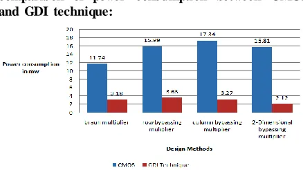
The 4x4 braun multiplier is designed in CMOS by using 456 transistors and power consumption of 4x4 braun multiplier in CMOS is 11.74mw.
Fig. 6: power consumption waveform of Braun
multiplier in CMOS
4x4 Row bypassing multiplier:
The 4x4 row bypassing multiplier is designed in CMOS by using 756 transistors and power consumption of 4x4 row bypassing multiplier in conventional method is 15.99mw.
Fig. 7: power consumption waveform of row bypassing
multiplier in CMOS
4x4 Column bypassing multiplier:
The 4x4 Column bypassing multiplier is designed in CMOS by using 582 transistors and power consumption of 4x4 Column bypassing multiplier in CMOS is 17.34mw.
Fig. 8: power consumption waveform of column
bypassing multiplier in CMOS
4X4 2-Dimensional bypassing multiplier:
The 4x4 Column bypassing multiplier is designed in CMOS by using 774 transistors and power consumption of 4x4 Column bypassing multiplier in CMOS is 15.81mw.
Fig. 9: power consumption of 4x4 Column bypassing
multiplier in CMOS
GDI Technique:
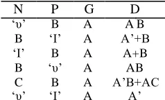
Gate-Diffusion-Input (GDI) method is based on the use of a simple cell as shown in figure .2. At a first glance the basic cell reminds the standard CMOS inverter, but there are some important differences: 1) GDI cell contains three inputs – G (common gate input of NMOS and PMOS), P (input to the source/drain of PMOS), and N (input to the source/drain of NMOS).
2) Bulks of both NMOS and PMOS are connected to N or P respectively, so it can be arbitrarily biased at contrast with CMOS inverter. It must be remarked, that not all the functions are possible in standard P-Well CMOS process, but can be successfully implemented in Twin-Well CMOS or SOI technologies .
Fig.10: GDI basic cell
Table: 1 shows how a simple change of the input configuration of the simple GDI cell corresponds to very different Boolean functions. Most of these functions are complex (6-12 transistors) in CMOS, as well as in standard PTL implementations, but very simple (only 2 transistors per function) in GDI design method.
Table: 1. some logic functions that can be implemented with a single GDI cell
N P G D
‘υ’ B A A’B
B ‘I’ A A’+B
‘I’ B A A+B
B ‘υ’ A AB
C B A A’B+AC
Int. J. Adv. Res. Sci. Technol. Volum e 3, Issue 4, 2014, pp.208-212
Fig. 11: transistor level implementation of and gate using GDI technique
Fig. 12: transistor level implementation of MUX using GDI technique
Fig. 13: transistor level implementation of half adder using GDI technique
Fig. 14: transistor level implementation of full adder using GDI technique
Implementing of Different Types of Multipliers Using GDI Technique:
4x4Braun multiplier:
The 4x4 bruan multiplier is designed in GDI technique by using 136 transistors and power consumption of 4x4 braun multiplier in GDI technique is 3.18mw.
Fig. 15: power consumption waveform of braun
multiplier in GDI Technique
4x4 Row bypassing multiplier:
The 4x4 row bypassing multiplier is designed in GDI technique by using 196 transistors and power consumption of 4x4 row bypassing multiplier in GDI technique is 3.63mw.
Fig. 16: power consumption waveform of row bypass
multiplier in GDI Technique
4x4 Column bypassing multiplier:
The 4x4 Column bypassing multiplier is designed in GDI technique by using 160 transistors and power consumption of 4x4 Column bypassing multiplier in GDI technique is 3.27mw.
Fig. 17: power consumption waveform of column
bypass multiplier in GDI Technique
4x4 2-Dimensional bypassing multiplier:
Int. J. Adv. Res. Sci. Technol. Volum e 3, Issue 4, 2014, pp.208-212
Fig. 18: power consumption waveform of 4x4 Column
bypassing multiplier in GDI technique
Comparison Results between Conventional Method and GDI Technique:
Area comparison between CMOS and GDI
technique:
Fig. 19: area comparison between CMOS and GDI
technique
comparison of power consumption between CMOS and GDI technique:
Fig. 20: power consumption between CMOS and
GDI technique
Conclusion:
By combining both row bypassing and column bypassing multipliers we have produced a 2-D bypassing multiplier with less area and power consumption.
Based on the simplification of the MAC operations and by using low-power bypassing technique, we have designed a two dimensional multiplier which has less computations and less switching activities with low power consumption.
References:
1.Oscal T. -C. Chen, Sandy Wang, and Yi-Wen Wu, .M inimization of Switching Activities of Partial Products for Designing Low-Power M ultipliers., IEEE Transactions on VLSI Systems, June 2003 vol. 11, no.3. 2.HichemBelhadj, BehroozZahiri, Albert Tai
.Power-sensitive design techniques on FPGA devices. Proceedings of International conference on IC Taipai (2003).
3.S. Hong, S. Kim, M .C. Papaefthymiou, and W.E. Stark, .Low power parallel multiplier design for DSP applications through coefficient optimization. In Proc. of Twelfth Annual IEEE Int. ASIC/SOC onf., Sep. 1999, pp. 286-290.