COMPUTER SCIENCE & TECHNOLOGY
www.computerscijournal.org
March 2013, Vol. 6, No. (1): Pgs. 93-101 An International Open Free Access, Peer Reviewed Research Journal
Published By: Oriental Scientific Publishing Co., India.
INTRODUCTION
After decades of watching the Moore's law hold and en-joying the steady increase in transistor densities, the pre- dominantly CMOS based Integrated Circuit industry now faces the prospect of transistor sizes hitting the physical limit. As sizes go well below the micro-scale, undesirable effects like high power dissipation and quantum-mechanical side-effects discourage further scaling down of CMOS devices. With the view of countering these problems, or putting these very effects to good use, many nanoelectronic fabrics are being explored to serve as an aid or replacement to CMOS devices1. One such option
-CoplanarWire Crossing based on Bayesian Scheme for QCA
K. JEYAKANTH
Latha Mathavan Engineering College, Madurai - 625 304, India.
(Received: February 26, 2013; Accepted: March 04, 2013)
ABSTRACT
QCA is one of the innovating technologies for Nano scale computation. With the present difficulties in reduction of sizes in transistor circuits, QCA has been proposed as a kind of replacement for such instances Researchers have developed several models for defect characterization and design to minimize the uncertainty of proper circuit operation. This uncertainty of the circuit aids in developing a probabilistic model for analysis. One such model is the Bayesian network (BN) modeling6, which exploits the causal relationships in clocked QCA circuits to obtain
a model with low complexity. It is based on density matrix formulations and also takes the dependencies induced by clocking of cells. One of the many interesting features of BN is that it not only captures the dependencies existing between two QCA cells, but can also be used to conduct steady stateoperations without the need for temporal computation of quantum mechanical equations.
Key words: Quantum cellular automata, QCADesigner, Simulation, Design,Bayesian network model.
Quantum-dot Cel- lular Automata - has been widely perceived as one of the technologies which can be a solution to the scaling prob- lems in CMOS technology. It uses charge orientation to represent logic rather than current flow2-3. The basic device
and OR gates are easily implemented by ûxing one of the inputs of the Majority gate at -1 and +1 respectively. Apart from its novel concept of operation, Quantum-dot Cellular Automata is considered to be a promising paradigm because of the high speeds and extremely low power consumption it promises.
working, illustrate its use with an example of a XOR gate and analyze its pros and cons. Section 5 describes a simulation engine for QCA created by the authors and the results of simulating designs which use the proposed wire crossing mechanism. We con- clude in Section 6.
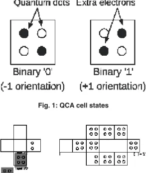
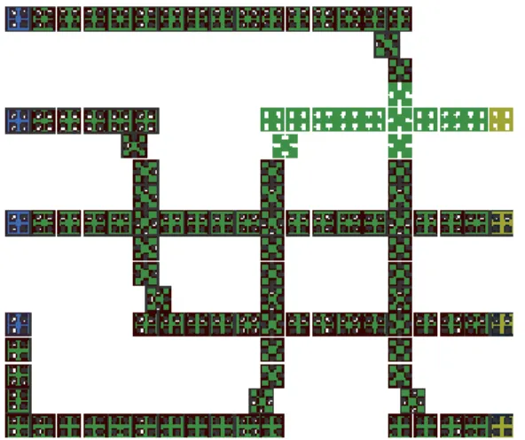
Fig. 1: QCA cell states
Fig. 2: Basic logic gates in QCA
However, quite a few issues need to be addressed before QCA can be considered as a replacement for CMOS in prac- tice. One such problem is that of crossing wires efûciently. While solutions to this problem have been proposed, each has its own shortcomings. In this paper, we propose a new mechanism for coplanar wire crossing, which is based on the clocking of cells. Not only is the proposed solution robust and easy to incorporate in designs, it enables the QCA fabric to be a simple, regular grid of only a single type of cells.
The paper is organized as follows : Sections 2 and 3 review the popular clocking mechanism used in QCA circuits, and the existing methods of crossing wires and previous work dealing with the problem respectively. In Section 4, we propose a new mechanism for coplanar wire crossing based on clocking of cells, detail its
Fig. 3: Landauer clocking signals for QCA
Conventional QCA Clocking
Clocking is a concept introduced with the objective of giving direction to the logic ûow in QCA circuits. A four phase clocking strategy is used to facilitate adiabatic switch- ing and thus a reliable circuit4. The control of ground- state by clocking
involves adjusting the tunneling barriers to ûx the electrons at their positions or let them tunnel to achieve ground-state. The four phases of this clocking scheme (Figure 3) are : SWITCH - the cell determines its next state according to neighbors’ states, HOLD - the bar- rier is set so that the electrons remain in the state it settled to during the SWITCH phase, RELEASE - the cell moves towards the NULL state, and RELAX - the barrier forces cell to the NULL state.
Wire Crossing in QCA
A number of methods have been explored to tackle the problem of wire crossings in QCA. We discuss these in this section.
Coplanar Wire Crossings
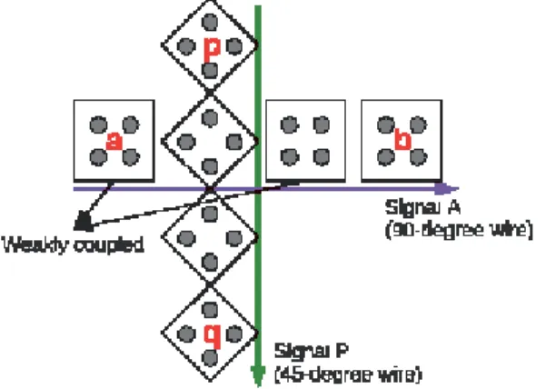
Coplanar wire crossings using a combination of 45- degree and 90-degree cells have long been projected as a unique feature of the QCA paradigm5. It is based on the observation
are one cell apart. Predictably, this coupling is somewhat weaker than it would have been in a normal wire, leaving the success of the crossing less probable.
for the crossing to remain reliable. Though a number of tricks (like TMR and thicker cross- ings7)
have been tried to improve the robustness of these crossings, it would always be preferable to have an inherently more reliable coplanar crossing occupying lesser area.
A more immediate issue associated with the coplanar wire crossing, perhaps, is the practical difûculty involved in fabricating molecular QCA circuits including cells of more than one orientation8. The need for cells to be placed at
half-cell displacements not only makes fabrication tougher, but makes the resulting circuits very much prone to defects.
Multilayer Wire Crossings
The concept of using multiple layers of QCA cells has been proposed as a way to overcome the difûculties of the coplanar wire crossings discussed above. However, it has not been demonstrated experimentally and may turn out to be infeasible to implement or highly dependant on the implementation. Fabrication issues too put the practical success of this method in doubt9.
Elimination of Wire Crossings
However, it should be noted that this may not be a very scalable solution, as the area overhead involved in node duplication increases exponentially with the size of the circuit. Also, the crossings are merely pushed to the input end of the circuit and may lead to a substantial increase in the number of inputs to the circuit if the QCA circuit is kept crossing free.
Fig. 4: Coplanar Wire Crossing Structure using combination of 45 and 90-deg wires
Being a never-seen-before phenomenon offered by QCA, this area and timing efûcient coplanar wire crossing has been highly popular. However, it comes with issues of low robustness and fabrication difûculties. The weak cou- pling makes the crossing highly sensitive to physical param- eters like cell dimension, inter-cellular spacing, temperature etc. In spite of the physical parameters being favorable, there are instances when a circuit with multiple crossings may behave unexpectedly. As illustrated in6, cascading wire
crossings may lead to floating sections of wire which are weakly coupled with the rest of the wire, and are vulnerable to crosstalk. High levels of precision in the placement of the cells are needed
Fig. 5:
Logical Wire Crossings
Swapping two bits using XOR gates has been explored as an option to perform wire crossings logically11. Though this approach
eliminates the problems of fabrication and re-liability, it introduces a signiûcant area overhead and in- volves a considerable delay.
Proposed Clocking Scheme
We propose an 8-phase clocking scheme with three types of clock signals - Normal, Crossing and Converting12. Four phase shifted versions of
the Normal clock signal are used for general logic ûow, a Crossing signal is used at the intersections of wire crossings and two phase shifted ver- sions of the Converting signals act as the interface between the two. The assignment of clock phases and the wave- forms in a typical wire crossing are as shown in Figures 5(a) and 5(b).
The four Normal clock phases behave similar to the conventional 4-phase clocking signals used in QCA and ensure that any type of logic is implementable with them. The Crossing and Converting signals are routing signals, mainly used at wire crossings.
This scheme makes it possible to use a regular grid of 90-degree cells to build any type of circuit. It paves the way for building more robust and less defective circuits by removing the need for multiple layers, multiple types of cells and different cell displacements.
Wire Crossing using Time DivisionMultiplexing The key idea behind the proposed scheme is to use the intersection cell to time-division multiplex the signals on the two crossing wires. The facts that a cell effectively sam- ples its neighborhood and determines its state only during its SWITCH phase and that cells in their RELAX phase do not affect the orientation of cells in the vicinity have been used to design the clocking patterns and the assignment of clock phases in the crossing.
A QCA clock cycle in this scheme consists of a cycle of the Normal, Converting signals, or two complete cycles of the Crossing signal.
All cells used for computation and normal signal prop- agation are assigned Normal clock signals. The Crossing cell samples the states of its neighbors twice in a clock cycle, thus carrying the values of two signals in two halves of the clock cycle. The Converting cells sample the state of the Crossing cell during the relevant part of the clock cycle to get the required wire’s signal. Now, a Normal cell in each direction can sample this signal to complete the wire crossing.
The working of a crossing is illustrated in Figure 5(b) with the signal values carried by each cell over two clock cycles or 16 phases of the clock. In this example, when x switches at phase-1, only one of its neighbors - a - is in the HOLD phase, resulting in x holding a(1) at phase-2. Cells b and c switching at phases 2 and 3 propagate this value. Now that the horizontal signal has been sent across, when x switches at phase-5, only p is in the HOLD phase and Cells q and r propagate the signal in the vertical wire intact. The arrows in Figure 5(b) show how the signal values travel from input to output on both wires. Note that, for each signal, only the neighbor from which the required signal is to be copied is in the HOLD phase, all others being in the RELAX phase.
We now move on to illustrate the usage of the proposed wire crossing mechanism using a 2-input XOR gate.
Example : XOR gate
A straightforward implementation of the expression A.B + B.A, using two inverters, two AND gates and an OR gate is considered. The layouts of the XOR gate implemented using the conventional coplanar crossings (Sec- tion 3.1) and the proposed coplanar crossing mechanism are provided for comparison in Figure 6.
However, the clocking-based crossing scheme requires the crossing signals to be clocked only with Normal-0 and Normal-2 and introduces a delay of 3 phases in the signals. This needs the cells to be clocked such that they are clocked with the correct clock signals when they arrive at crossings. In Figure 6(b), the first crossing has the signals A and B coming in clocked with Normal-2 and Normal-0 respectively. After the intersection, signal A is tapped using a cell clocked with Converting-1 and trans- ferred to the wire leading to the inverter at Normal-0. Sim- ilarly, signal B is tapped and forwarded using cells clocked with Converting-0 and Normal-1 respectively. The second crossing has the signals A and B coming in with Normal-0 and Normal-2 respectively. They are tapped out of the crossing in a fashion similar to that employed in the first crossing.
From the layouts in Figure 6, it is clear
that the areas of the circuits are comparable. In fact, the circuit using the proposed crossing mechanism uses fewer cells. However, the circuit in Figure 6(b) has a latency of two clock cycles while the latency of that in Figure 6(a) is only one clock cycle.
Analysis of the Scheme
The main constraint that the proposed crossing method imposes on circuit design is that the input cells at the crossings should have a phase difference of π. To be able to meet this constraint with the least delay overhead, a full-fledged 8-phase clocking scheme involving 8-phase shifted versions (with phase difference of π/4) of each type of clock signal can be used. Though it would lead to increased flexibility, it would need 20 (8 Normal,4 Crossing and 8 Converting ) different types of clock signals to be distributed throughout the circuit. Thus, a trade-off exists between flexibility/delay and ease of implementation. We suggest that the inputs to the crossing be restricted to be clocked only with Normal- 0 and Normal-2, allowing any circuit to be designed with only 7 types of clock signals.
It should be remembered that the delay inherent in the crossing and the delays introduced by the need to keep the inputs clocked with only Normal-0 and Normal-2 may in- crease the delay of the circuit compared to if wire crossings were implemented in any of the old methods. However, this proves to be a favorable option compared to dealing with the complex fabrication requirements and lack of robustness.
Another point to be noted is that, the use of the pro- posed crossing method may lead to compact and simple designs. We believe that, in larger circuits, the area over- head in crossing wires using a combination of the 45degree and 90degree cells -for conversion between signals on 45- degree and 90-degree wires - would be reduced by a good factor when the proposed method of wire crossing is used. It may also lead to decrease in wire lengths, allowing the use of higher clock frequencies. Also, in cases where delay is a constraint, a combination of this wire crossing method and elimination of wire crossings can be employed to reach area and delay constraint goals.
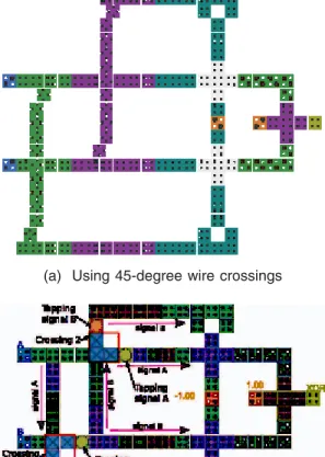
(a) Using 45-degree wire crossings
(b) Using proposed wire crossings
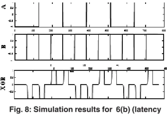
The bistable engine of this simulator is based on the same assumptions and default settings as QCADesigner. Figure 8 shows the results of simulating the layout in Figure 6(b).
Though the main utility of the Crossing and Convert ing signals is to enable coplanar wire crossings, they may be employed to implement logic or skip the distance generally required between two turning wires, merge two wires to simplify routing etc.
do not involve wire crossings however high the number of time steps being used. The MATLAB simu- lation engine built by the authors is able to simulate all such circuits well to give the results as expected from the logical design of the circuit, thus proving to be more accurate. Also, the bistable engine of the MATLAB simulator proves to be faster than QCADesigner, mostly due to its needing far fewer number of simulation steps to achieve the same accuracy. For instance, with simulation conditions remain ing the same, while the accurate simulation of the circuit in Figure 6(a) takes 5s in QCADesigner, it takes only 0.52s in the MATLAB simulator.
The layout of an arbitrary circuit with six wire cross- ings using wire crossings based on 45-degree cells shown in Figure 9(a). While QCADesigner fails to simulate this design accurately (Figure 9(b)), the MATLAB simulation engine is able to simulate it correctly. However, as pointed out in [6], the circuit experiences crosstalk when a cell of ûxed polarity(-1) is introduced as in Figure 9(c). This shows that coplanar wire crossings as described in Section 3.1 are indeed vulnerable and not robust. In contrast to this, the same circuit using the proposed crossing mechanism (Fig- ure 9(c)) is not affected by the fixed polarity cell, as seen from its simulation waveform in Figure 9(d). Thus, the proposed coplanar wire crossing conventional coplanar wire crossing method.
DISCUSSION
We propose a bayesian metwork based modeling and interference for the QCAcell Fig. 7: Specialized use of clocking
scheme to simplify XOR gate
One interesting use of the clocking-based coplanar clocking scheme is illustrated in Figure 7. In this circuit, instead of limiting the use of the Crossing cells to the in- tersections of wire crossings, they are used to construct a wire which carries both the input signals - A and B. This minor extension of the wire crossing idea lets us tap the signals any number of times out of the “Crossing Channel”. In this particular example, the two crossings in Figure 6(b) are merged into one, resulting in a reduction in the area and the latency of the circuit. Further investigation is necessary to explore further possible uses of this clocking scheme.
Simulation
The simulations of the designs in this paper were done using a MATLAB based simulation engine developed by the authors. It has been developed after noting that QCADe signal13 does
not scale well, especially with increase in the number of wire crossings in the circuit.
There are quite a few instances of QCADesigner not being able to provide the expected simulation results even for circuits which
(a) Using 45-degree wires (b) Simulation results for 9(a) using QCADesigner
(c) Using proposed clocking d) Simulation results for 9(c) (latency of 2 cycles)
using MAT- LAB simulator
Fig. 9: Circuit with a number of wire crossings
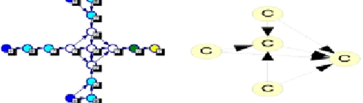
polarization. A big Bayesian network is a directed acyclic graph(DAG) in which the nodes of the network represent random variables and a set of directed link connect pairs of nodes the exact joint variable probapility equation is given by
P(x5, x4, x3, x2, x1) = P(x5|x4, x3, x2, x1) P(x4|x3, x2, x1)P(x3|x2, x1) P(x2|x1)P(x1)
In this BN, the random variable X5 is independent of X1,the conditional independenc is expressed as
P(x5|x4, x3, x2, x1) = P(x5|x4)
Fig : Block diagram of BN Fig: Majority Gate Fig: Clocked majority
CONCLUSION
This work shows that coplanar wire crossings are feasi- ble with a single type of cells, enabling the use of a regular grid of QCA cells. Apart from simplifying fabrication requirements, the proposed scheme for coplanar wire crossings
leads to more robust and compact designs, the quantive- cation of which, needs further investigation.
Dynamic BN would be useful in analyzing both Spatial & temporial behaviour of QCA circuit for defects & reliable operation under physical and environmental variation
REFERENCES
1. International Technology Roadmap for Semiconductors, (ITRS) 2004,. http:// public.itrs.net.
2. C. Lent and P. Tougaw. A device architecture for computing with quantum dots. Proceedings of the IEEE, 85(4):541-557 (1997).
3. C. S. Lent. Molecular quantum-dot cellular automata. (2006).
4. C. Lent and B. Isaksen. Clocked molecular quantum-dot cellular automata. Electron Devices, IEEE Transactions on, 50 (9):1890-1896 (2003).
5. P. D. Tougaw and C. S. Lent. Logical devices imple- mented using quantum cellular automata. Journal of Applied Physics, 75:1818–1825 (1994).
6. K. Walus and G. A. Jullien. Design tools for
an emerging soc technology: Quantum-dot cellular automata. Proceedings of the IEEE, 94(6):1225–1244 (2006).
7. S. Bhanja, M. Ottavi, F. Lombardi, and S. Pontarelli. Novel designs for thermally robust coplanar crossing in qca. 1: 6 (2006). 8. M. Crocker, M. Niemier, X. S. Hu, and M. Lieberman. Molecular qca design with chemically reasonable con- straints. J. Emerg. Technol. Comput. Syst., 4(2): 1-21 (2008).
M. Niemier, and R. Ravichandran. Eliminating wire crossings for molec- ular quantum-dot cellular automata implementation. 565–571 (2005).
11. M. Niemier, P. Kogge, R. Mur phy, A. Rodrigues, T. Dysart, and S. Frost. Dataûow in molecular qca: Logic can “sprint”, but the memory wall can still be a
“hurdle”, 2006. http://www.cse.nd.edu/ Reports/2006/TR-2006-14.pdf.