MODULE 2: TABLE OF CONTENTS
ANALOG-TO-DIGITAL CONVERSION PCM Sampling Sampling Rate Quantization Quantization Levels Quantization ErrorUniform vs. Non Uniform Quantization Encoding
Original Signal Recovery PCM Bandwidth
Maximum Data Rate of a Channel Minimum Required Bandwidth TRANSMISSION MODES PARALLEL TRANSMISSION SERIAL TRANSMISSION Asynchronous Transmission Synchronous Transmission Isochronous
DIGITAL TO ANALOG CONVERSION
Aspects of Digital to Analog Conversion Amplitude Shift Keying (ASK)
Binary ASK (BASK)
Implementation of BASK Bandwidth for ASK Frequency Shift Keying (FSK)
Binary FSK (BFSK)
Implementation of BFSK Bandwidth for BFSK Phase Shift Keying (PSK)
Binary PSK (BPSK)
Quadrature Amplitude Modulation (QAM) Bandwidth for QAM
MULTIPLEXING
Frequency Division Multiplexing (FDM) Multiplexing Process
Demultiplexing Process Applications of FDM
The Analog Carrier System Wavelength-Division Multiplexing (WDM) Time Division Multiplexing (TDM)
Synchronous TDM
Time Slots and Frames Interleaving
Empty Slots
Data Rate Management Frame Synchronizing Statistical TDM
SPREAD-SPECTRUM
Frequency Hopping Spread Spectrum (FHSS) Bandwidth Sharing
Direct Sequence Spread Spectrum (DSSS) Bandwidth Sharing
SWITCHING
Three Methods of Switching
Switching and TCP/IP Layers CIRCUIT SWITCHED NETWORK
Three Phases
Efficiency Delay
PACKET SWITCHED NETWORK Datagram Networks
Routing Table
Destination Address Efficiency
Virtual Circuit Network Addressing Three Phases
Data Transfer Phase Setup Phase
Setup Request Teardown Phase
Efficiency
CHAPTER 5
5.1 DIGITAL-TO-ANALOG CONVERSION
Digital-to-analog conversion is the process of changing one of the characteristics of an analog signal based on the information in digital data. Figure 5.1 shows the relationship between the digital information, the digital-to-analog modulating process, and the resultant analog signal.
FIGURE Digital-to-analog conversion
A sine wave is defined by three characteristics: amplitude, frequency,and phase. When we vary anyone of these characteristics, we create a different version of thatwave. So, by changing one characteristic of a simple electric signal, we can use it to represent digital data. Any of the three characteristics can be altered in this way, giving us at least three mechanisms for modulating digital data into an analog signal: amplitude shift keying (ASK),frequency shift keying (FSK), and phase shift keying (PSK). In addition, there is a fourth (and better) mechanism that combines changing both the amplitude and phase, called quadrature amplitude modulation (QAM). QAM is the most efficient of these options and is the mechanism
commonly used today.
5.1.1 Aspects of Digital-to-Analog Conversion
Before we discuss specific methods of digital-to-analog modulation, two basic issues must bereviewed: bit and baud rates and the carrier signal.
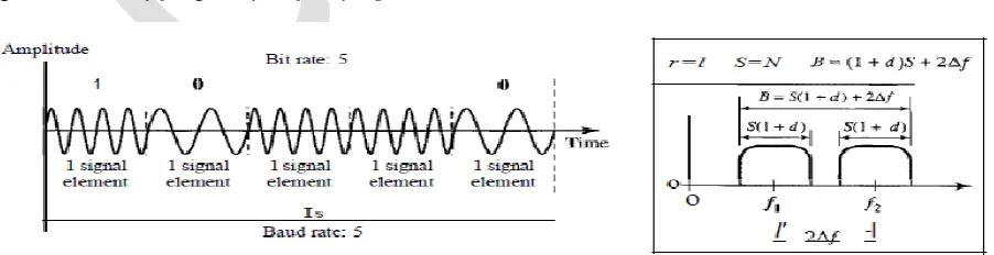
Data Element Versus Signal Element We defined a data element as the smallest piece of information to be exchanged, the bit. We also defined asignal element as the smallest unit of a signal that is constant.The nature of the signal element is a little bit differentin analog transmission.
Data Rate Versus Signal Rate
S=Nx1/r baud
where N is the data rate (bps) and r is the number of data elements carried in one signal element.The value of r in analog transmission is r =log2 L, where L is the type of signal element, not the level. The same nomenclature is used to simplify the comparisons.
Example 5.1
An analog signal carries 4 bits per signal element. If 1000 signal elements are sent per second, find the bit rate.
Solution
In this case, r = 4, S = 1000, and N is unknown. We can find the value ofN from S=Nx1/r
or N=Sxr= 1000 x 4 =4000 bps
Example 5.2
An analog signal has a bit rate of 8000 bps and a baud rate of 1000 baud. How many dataelements are carried by each signal element? How many signal elements do we need?
Solution
In this example, S = 1000, N =8000, and rand L are unknown. We find first the value of randthen the value of L.
S=Nx1/r r=N/S=8000/1000=8 bits/baud r= log2L L= 2 r
=2 8 =256
Bandwidth
The required bandwidth for analog transmission of digital data is proportional to the signal rate except for FSK, in which the difference between the carrier signals needs to be added. Wediscuss the bandwidth for each technique.
Carrier Signal
In analog transmission, the sending device produces a high-frequency signal that acts as a base for the information signal. This base signal is called the carrier signal or carrier frequency. The receiving device is tuned to the frequency of the carrier signal that it expects from the sender.Digital information then changes the carrier signal by modifying one or more of its characteristics (amplitude, frequency, or phase). This kind of modification is called modulation(shift keying).
5.1.2Amplitude Shift Keying
In amplitude shift keying, the amplitude of the carrier signal is varied to create signal elements. Both frequency and phase remain constant while the amplitude changes.
Binary ASK (BASK)
ASK is normally implemented using only two levels. This is referred to as binary amplitude shiftkeying or on-off keying (OOK). The peak amplitude of one signal level is 0; the other is the same as the amplitude of the carrier frequency. Figure 5.3gives a conceptual view of binary ASK.
Bandwidth for ASK Figure 5.3 also shows the bandwidth for ASK. Although the carrier signal is only one simple sine wave, the process of modulation produces a nonperiodic composite signal.As we expect, the bandwidth is proportional to the signal rate (baud rate). However, there is normally another factor involved, called d, which depends on the modulation and filtering process. The value of d is between 0 and 1. This means that the bandwidth can be expressed as shown, where 5 is the signal rate and the B is the bandwidth.
B =(1 +d) x S
The formula shows that the required bandwidth has a minimum value of S and a maximum value of 2S. The most important point here is the location of the bandwidth.
The middle of the bandwidth is where fc, the carrier frequency, is located. This means if we have a bandpass channel available, we can choose our fcso that the modulated signal occupies that bandwidth.
This is in fact the most important advantage of digital to- analog conversion. We can shift the resulting bandwidth to match what is available.
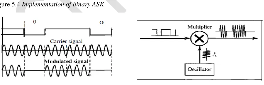
Figure 5.4 shows how we can simply implement binary ASK.
If digital data are presented as a unipolar NRZ digital signal with a high voltage of I V and a low voltage of 0 V, the implementation can achieved by multiplying the NRZ digital signal by the carrier signal coming from an oscillator. When the amplitude of the NRZ signal is 1, the amplitude of the carrier frequency is held; when the amplitude of the NRZ signal is 0, the amplitude of the carrier frequency is zero.
Figure 5.4 Implementation of binary ASK
Example 5.3
We have an available bandwidth of 100 kHz which spans from 200 to 300 kHz. What are the carrier frequency and the bit rate if we modulated our data by using ASK with d =1?
The middle of the bandwidth is located at 250 kHz. This means that our carrier frequency can be at fc =250 kHz. We can use the formula for bandwidth to find the bit rate (with d =1 and r =1). B =(l +d) x S=2 x N x1/r=2 xN =100 kHz ... N =50 kbps
Example 5.4
In data communications, we normally use full-duplex links with communication in both directions. We need to divide the bandwidth into two with two carrier frequencies, as shown in Figure 5.5. The figure shows the positions of two carrier frequencies and the bandwidths.The available bandwidth for each direction is now 50 kHz, which leaves us with a data rate of 25 kbps in each direction.
Figure 5.5 Bandwidth of full-duplex ASK used in Example 5.4
Multilevel ASK
The above discussion uses only two amplitude levels. We can have multilevel ASK in which there are more than two levels. We can use 4,8, 16, or more different amplitudes for the signal and modulate the data using 2, 3, 4, or more bits at a time. In these cases, r = 2, r = 3, r =4, and so on. Although this is not implemented with pure ASK, it is implemented with QAM (as we will see later).
Frequency Shift Keying
In frequency shift keying, the frequency of the carrier signal is varied to represent data. The frequency of the modulated signal is constant for the duration of one signal element, but changes for the next signal element if the data element changes. Both peak amplitude and phase remain constant for all signal elements
Binary FSK (BFSK) One way to think about binary FSK (or BFSK) is to consider two carrier frequencies. In Figure 5.6, we have selected two carrier frequencies,f1 and f2. We use the first carrier if the data element is 0; we use the second if the data element is 1.
Figure 5.6 Binary frequency shift keying
As Figure 5.6 shows, the middle of one bandwidth is f1 and the middle of the other is f2. Both f1 and
Bandwidth for BFSK Figure 5.6 also shows the bandwidth of FSK. Again the carrier signals are only simple sine waves, but the modulation creates a nonperiodic composite signal with continuous frequencies. We can think of FSK as two ASK signals, each with its own carrier frequency f1 and f2). If the difference between the two frequencies is 2∆f, then the required bandwidth is
B=(l+d) x S+2∆f.
What should be the minimum value of 2∆f.? In Figure 5.6, we have chosen a value greater than (l +
d)S. It can be shown that the minimum value should be at least S for the proper operation of modulation and demodulation.
Example 5.5
We have an available bandwidth of 100 kHz which spans from 200 to 300 kHz. What should be the carrier frequency and the bit rate if we modulated our data by using FSK with d =1?
Solution
This problem is similar to Example 5.3, but we are modulating by using FSK. The midpoint of the band is at 250 kHz. We choose 2∆f to be 50 kHz; this means
B =(1 + d) x S + 2∆f=100 . 2S =50 kHz S = 25 kbaud N= 25 kbps
Compared to Example 5.3, we can see the bit rate for ASK is 50 kbps while the bit rate for FSK is 25 kbps.
Implementation There are two implementations of BFSK: noncoherent and coherent. In noncoherent BFSK, there may be discontinuity in the phase when one signal element ends and the next begins. In coherent BFSK, the phase continues through the boundary of two signal elements. Noncoherent BFSK can be implemented by treating BFSK as two ASK modulations and using two carrier frequencies. Coherent BFSK can be implemented by using one voltage-controlled oscillator
(VeO) that changes its frequency according to the input voltage. Figure 5.7 shows the simplified idea behind the second implementation. The input to the oscillator is the unipolar NRZ signal. When the amplitude of NRZ is zero, the oscillator keeps its regular frequency; when the amplitude is positive, the frequency is increased.
Figure 5.7 Implementation ofBFSK
Multilevel FSK
frequencies need to be 2∆f apart. For the proper operation of the modulator and demodulator, it can
be shown that the minimum value of 2∆f needs to be S. We can show that the bandwidth with d =0 is
B= (l +d) x S + (L - 1) 2∆f B =Lx S
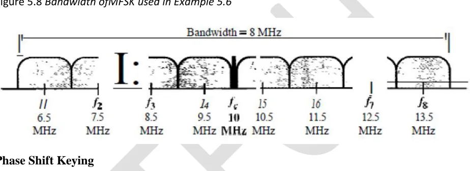
Example 5.6
We need to send data 3 bits at a time at a bit rate of 3 Mbps. The carrier frequency is 10 MHz. Calculate the number of levels (different frequencies), the baud rate, and the bandwidth.
Solution We can have L =23 =8. The baud rate is S =3 MHz/3 =1000 Mbaud. This means that the carrier frequencies must be 1MHz apart (2∆f=1 MHz). The bandwidth is B=8 x 1000 =8000. Figure 5.8 shows the allocation of frequencies and bandwidth.
Figure 5.8 Bandwidth ofMFSK used in Example 5.6
Phase Shift Keying
In phase shift keying, the phase of the carrier is varied to represent .two or more different signal elements. Both peak amplitude and frequency remain constant as the phase changes. Today, PSK is more common than ASK or FSK. QAM, which combines ASK and PSK, is the dominant method of digital-to- analog modulation.
Binary PSK (BPSK)
In ASK, the criterion for bit detection is the amplitude of the signal; in PSK, it is the phase. Noise can change the amplitude easier than it can change the phase. In other words, PSK is less susceptible to noise than ASK.PSK is superior to FSK because we do not need two carrier signals.
Bandwidth
Figure 5.9 also shows the bandwidth for BPSK. The bandwidth is the same as that for binary ASK, but less than that for BFSK. No bandwidth is wasted for separating two carrier signals.
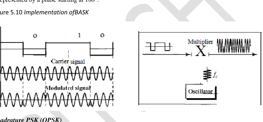
Implementation
The implementation of BPSK is as simple as that for ASK. The reason is that the signal element with phase 180° can be seen as the complement of the signal element with phase 0°. This gives us a clue on how to implement BPSK. We use the same idea we used for ASK but with a polar NRZ signal instead of a unipolar NRZ signal, as shown in Figure 5.10. The polar NRZ signal is multiplied by the carrier frequency; the 1 bit (positive voltage) is represented by a phase starting at 0°; the 0 bit (negative voltage) is represented by a phase starting at 180°.
Figure 5.10 Implementation ofBASK
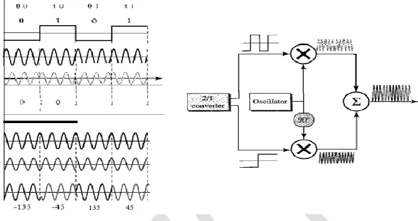
Quadrature PSK (QPSK)
The simplicity of BPSK enticed designers to use 2 bits at a time in each signal element, thereby decreasing the baud rate and eventually the required bandwidth. The scheme is called quadrature PSK or QPSK because it uses two separate BPSK modulations; one is in-phase, the other quadrature (out-of-phase).
The incoming bits are first passed through a serial-to-parallel conversion that sends one bit to one modulator and the next bit to the other modulator. If the duration of each bit in the incoming signal is T, the duration of each bit sent to the corresponding BPSK signal is 2T. This means that the bit to each BPSK signal has one-half the frequency of the original signal. Figure 5.11 shows the idea.
The two composite signals created by each multiplier are sine waves with the same frequency, but different phases. When they are added, the result is another sine wave, with one of four possible phases:
45°, -45°, 135°, and -135°. There are four kinds of signal elements in the output signal (L = 4), so we can
Example 5.7 Find the bandwidth for a signal transmitting at 12 Mbps for QPSK. The value of d =O.
Solution
For QPSK, 2 bits is carried by one signal element. This means that r =2. So the signal rate (baud rate) is S =N x (1/r) =6 Mbaud. With a value of d =0, we have B =S =6 MHz.
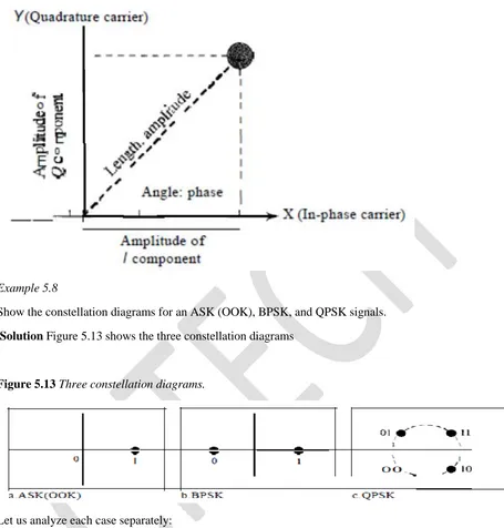
Constellation Diagram
A constellation diagram can help us define the amplitude and phase of a signal element, particularly when we are using two carriers (one in-phase and one quadrature), The diagram is useful when we are dealing with multilevel ASK, PSK, or QAM. In a constellation diagram, a signal element type is represented as a dot. The bit or combination of bits it can carry is often written next to it.
The diagram has two axes. The horizontal X axis is related to the in-phase carrier; the vertical Y axis is related to the quadrature carrier. For each point on the diagram, four pieces of information can be deduced. The projection of the point on the X axis defines the peak amplitude of the in-phase component; the projection of the point on the Y axis defines the peak amplitude of the quadrature component. The length of the line (vector) that connects the point to the origin is the peak amplitude of the signal element (combination of the X and Y components); the angle the line makes with the X axis is the phase of the signal element. All the information we need, can easily be found on a constellation diagram. Figure 5.12 shows a constellation diagram.
Example 5.8
Show the constellation diagrams for an ASK (OOK), BPSK, and QPSK signals.
Solution Figure 5.13 shows the three constellation diagrams
Figure 5.13 Three constellation diagrams.
Let us analyze each case separately:
a. For ASK, we are using only an in-phase carrier. Therefore, the two points should be on the X axis. Binary 0 has an amplitude of 0 V; binary 1 has an amplitude of 1V (for example). The points are located at the origin and at 1 unit.
b. BPSK also uses only an in-phase carrier. However, we use a polar NRZ signal for modulation. It creates two types of signal elements, one with amplitude 1 and the other with amplitude -1. This can be stated in other words: BPSK creates two different signal elements, one with amplitude I V and in phase and the other with amplitude 1V and 1800 out of phase.
elements have an amplitude of 21/2, but their phases are different (45°, 135°, -135°, and -45°). Of course, we could have chosen the amplitude of the carrier to be 1/(21/2) to make the final amplitudes 1 V.
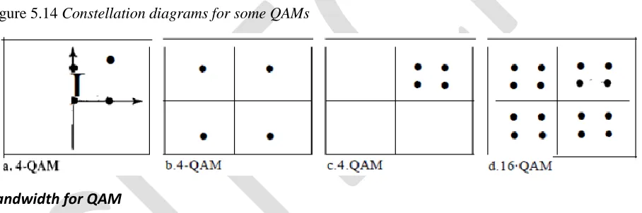
Quadrature Amplitude Modulation
PSK is limited by the ability of the equipment to distinguish small differences in phase. This factor limits its potential bit rate. So far, we have been altering only one of the three characteristics of a sine wave at a time; but what if we alter two? Why not combine ASK and PSK? The idea of using two carriers, one in-phase and the other quadrature, with different amplitude levels for each carrier is the concept behind quadrature amplitude modulation (QAM).
The possible variations of QAM are numerous. Figure 5.14 shows some of these schemes. Figure 5.14a shows the simplest 4-QAM scheme (four different signal element types) using a unipolar NRZ signal to modulate each carrier. This is the same mechanism we used for ASK (OOK). Part b shows another 4-QAM using polar NRZ, but this is exactly the same as QPSK. Part c shows another 4-QAM-4 in which we used a signal with two positive levels to modulate each of the two carriers. Finally, Figure 5.14d shows a 16-QAM constellation of a signal with eight levels, four positive and four negative.
Figure 5.14 Constellation diagrams for some QAMs
Bandwidth for QAM
The minimum bandwidth required for QAM transmission is the same as that required for ASK and PSK transmission. QAM has the same advantages as PSK over ASK.
CHAPTER 6
BANDWIDTH UTILIZATION : MULTIPLEXING AND SPREAD
SPECTRUM
6.1 MULTIPLEXING
bandwidth far in excess of that needed for the average transmission signal. If the bandwidth of a link is greater than the bandwidth needs of the devices connected to it, the bandwidth is wasted. An efficient system maximizes the utilization of all resources;bandwidth is one of the most precious resources we have in data communications.
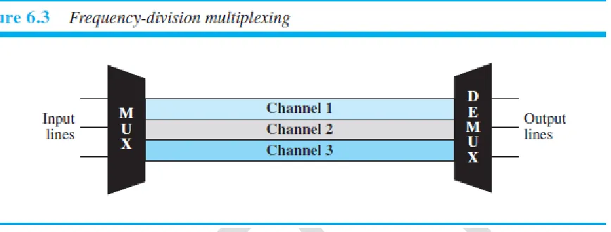
In a multiplexed system, n lines share the bandwidth of one link. Figure 6.1 shows the basic format of a multiplexed system. The lines on the left direct their transmission streams to a multiplexer(MUX), which combines them into a single stream (many-toone). At the receiving end, that stream is fed into a demultiplexer (DEMUX), which separates the stream back into its component transmissions (one-to-many) and directs them to their corresponding lines. In the figure, the word link refers to the physical path. The word channel refers to the portion of a link that carries a transmission between a given pair of lines. One link can have many (n) channels.
Figure 6.1 Dividing a link into channels
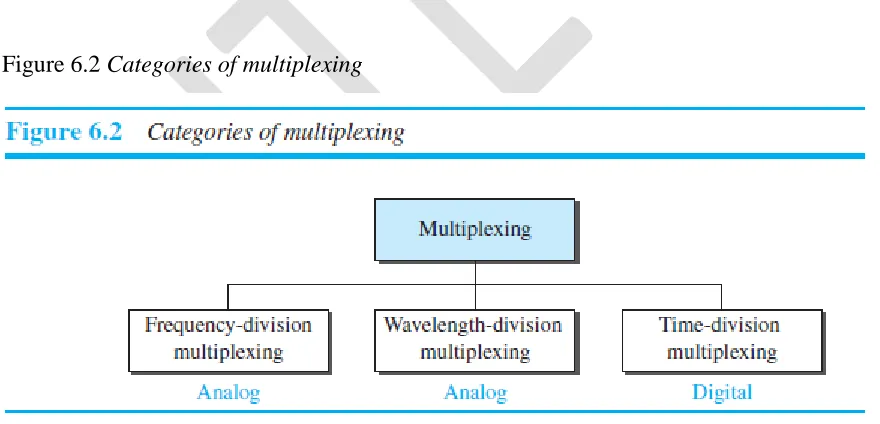
There are three basic multiplexing techniques: frequency-division multiplexing, wavelength-division multiplexing, and time-wavelength-division multiplexing. The first two are techniques designed for analog signals, the third, for digital signals (see Figure 6.2).
Figure 6.2 Categories of multiplexing
Frequency-Division Multiplexing
accommodate the modulated signal. These bandwidth ranges are the channels through which the various signals travel. Channels can be separated by strips of unused bandwidth-guard bands-to prevent signals from overlapping. In addition, carrier frequencies must not interfere with the original data frequencies. Figure 6.3 gives a conceptual view of FDM. In this illustration, the transmission path is divided into three parts, each representing a channel that carries one transmission.
We consider FDM to be an analog multiplexing technique; however, this does not mean that FDM cannot be used to combine sources sending digital signals. A digital signal can be converted to an analog signal before FDM is used to multiplex them.
Multiplexing Process
Figure 6.4 is a conceptual illustration of the multiplexing process. Each source generates a signal of a similar frequency range. Inside the multiplexer, these similar signals modulates different carrier frequencies (/1,12, and h). The resulting modulated signals are then combined into a single composite signal that is sent out over a media link that has enough bandwidth to accommodate it.
Demultiplexing Process
The Analog Carrier System
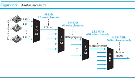
Figure 6.9 Analog hierarchy
In this analog hierarchy, 12 voice channels are multiplexed onto a higher-bandwidth line to create a group. A group has 48 kHz of bandwidth and supports 12 voice channels. At the next level, up to five groups can be multiplexed to create a composite signal called a supergroup. A supergroup has a bandwidth of 240 kHz and supports up to 60 voice channels. Supergroups can be made up of either five groups or 60 independent voice channels. At the next level, 10 supergroups are multiplexed to create a master group. A master group must have 2.40 MHz of bandwidth, but the need for guard bands between the supergroups increases the necessary bandwidth to 2.52 MHz. Master groups support up to 600 voice channels. Finally, six master groups can be combined into a jumbo group. A jumbo group must have 15.12 MHz (6 x 2.52 MHz) but is augmented to 16.984 MHz to allow for guard bands between the master groups.
Wavelength-Division Multiplexing
Wavelength-division multiplexing (WDM) is designed to use the high-data-rate capability of fiber-optic cable.
The optical fiber data rate is higher than the data rate of metallic transmission cable. Using a fiber-optic cable for one single line wastes the available bandwidth. Multiplexing allows us to combine several lines into one.
Figure 6.10 gives a conceptual view of a WDM multiplexer and demultiplexer. Very narrow bands of light from different sources are combined to make a wider band of light. At the receiver, the signals are separated by the demultiplexer
Figure 6.10 Wavelength-division multiplexing
Although WDM technology is very complex, the basic idea is very simple. We want to combine multiple light sources into one single light at the multiplexer and do the reverse at the demultiplexer. The combining and splitting of light sources are easily handled by a prism. A prism bends a beam of light based on the angle of incidence and the frequency. Using this technique, a multiplexer can be made to combine several input beams of light, each containing a narrow band of frequencies, into one output beam of a wider band of frequencies. A demultiplexer can also be made to reverse the process. Figure 6.11 shows the concept.
Time-Division Multiplexing
Figure 6.12 gives a conceptual view of TDM. Note that the same link is used as in FDM; here, however,the link is shown sectioned by time rather than by frequency. In the figure, portions of signals 1, 2, 3, and 4 occupy the link sequentially.
All the data in a message from source 1 always go to one specific destination, be it 1, 2, 3, or 4. The delivery is fixed and unvarying, unlike switching. We also need to remember that TDM is, in principle, a digital multiplexing technique.
Digital data from different sources are combined into one timeshared link. However, this does not mean that the sources cannot produce analog data; analog data can be sampled,changed to digital data, and then multiplexed by using TDM. We can divide TDM into two different schemes: synchronous and statistical
In synchronous TDM, the data flow of each input connection is divided into units, where each input occupies one input time slot. A unit can be 1 bit, one character, or one block of data. Each input unit becomes one output unit and occupies one output time slot.
The duration of an output time slot is n times shorter than the duration of an input time slot. If an input time slot is T s, the output time slot is Tin s where n is the number of connections. In other words, a unit in the output connection has a shorter duration; it travels faster. Figure 6.13 shows an example of synchronous TDM where n is 3.
In synchronous TDM, a round of data units from each input connection is collected into a frame . If we have n connections, frames divided into n time slots and one slot is allocated for each unit, one for each input line.
Time slots are grouped into frames. A frame consists of one complete cycle of time slots, with one slot dedicated to each sending device. In a system with n input lines, each frame has n slots, with each slot allocated to carrying data from a specific input line.
Interleaving
Empty Slots
Synchronous TDM is not as efficient as it could be. If a source does not have data to send, the corresponding slot in the output frame is empty. Figure 6.18 shows a case in which one of the input lines has no data to send and one slot in another input line has discontinuous data.
The first output frame has three slots filled, the second frame has two slots filled, and the third frame has three slots filled. No frame is full. We learn in the next section that statistical TDM can improve the efficiency by removing the empty slots from the frame.
Data Rate Management
One problem with TDM is how to handle a disparity in the input data rates. In all our discussion so far, we assumed that the data rates of all input lines were the same. However, if data rates are not the same, three strategies, or a combination of them, can be used. We call these three strategies multilevel multiplexing, multiple-slot allocation, and pulse stuffing.
Multilevel Multiplexing Multilevel multiplexing is a technique used when the data rate of an input line is a multiple of others. For example, in Figure 6.19, we have two inputs of 20 kbps and three inputs of 40 kbps. The first two input lines can be multiplexed together to provide a data rate equal to the last three. A second level of multiplexing can create an output of 160 kbps.
of another input. In Figure 6.20, the input line with a SO-kbps data rate can be given two slots in the output. We insert a serial-to-parallel converter in the line to make two inputs out of one.
Pulse Stuffing Sometimes the bit rates of sources are not multiple integers of each other. Therefore, neither of the above two techniques can be applied. One solution is to make the highest input data rate the dominant data rate and then add dummy bits to the input lines with lower rates. This will increase their rates. This technique is called pulse stuffing, bit padding, or bit stuffing. The idea is shown in Figure 6.21. The input with a data rate of 46 is pulse-stuffed to increase the rate to 50 kbps. Now multiplexing can take place.
Digital Signal Service
Table 6.1 DS and T line rates
The T-l line is used to implement DS-l; T-2 is used to implement DS-2; and so on. As you can see from Table 6.1, DS-O is not actually offered as a service, but it has been defined as a basis for reference purposes.
T Lines for Analog Transmission
Figure 6.24 T-l line for multiplexing telephone lines
The T-1 Frame As noted above, DS-l requires 8 kbps of overhead. To understand how this overhead is calculated, we must examine the format of a 24-voice-channel frame. The frame used on a T-l line is usually 193 bits divided into 24 slots of 8 bits each plus 1 extra bit for synchronization (24 x 8 + 1 = 193); see Figure 6.25. In other words, each slot contains one signal segment from each channel; 24 segments are interleaved in one frame. If a T-1 line carries 8000 frames, the data rate is 1.544 Mbps (193 × 8000 =1.544 Mbps)—the capacity of the line.
E Lines Europeans use a version of T lines called E lines. The two systems are conceptually identical, but their capacities differ. Table 6.2 shows the E lines and their capacities.
Statistical Time-Division Multiplexing
In synchronous TDM, each input has a reserved slot in the output frame. This can be inefficient if some input lines have no data to send.In statistical time-division multiplexing, slots are dynamically allocated to improve bandwidth efficiency. Only when an input line has a slot's worth of data to send is it given a slot in the output frame. In statistical multiplexing, the number of slots in each frame is less than the number of input lines. The multiplexer checks each input line in round robin fashion; it allocates a slot for an input line if the line has data to send; otherwise, it skips the line and checks the next line. Figure 6.26 shows a synchronous and a statistical TDM example. In the former, some slots are empty because the corresponding line does not have data to send. In the latter, however, no slot is left empty as long as there are data to be sent by any input line.
Addressing
Figure 6.26 also shows a major difference between slots in synchronous TDM and statistical TDM.
An output slot in synchronous TDM is totally occupied by data; in statistical TDM, a slot needs to carry data as well as the address of the destination.
Slot Size
Since a slot carries both data and an address in statistical TDM, the ratio of the data size to address size must be reasonable to make transmission efficient. For example, it would be inefficient to send 1 bit per slot as data when the address is 3 bits. This would mean an overhead of 300 percent. In statistical TDM, a block of data is usually many bytes while the address is just a few bytes.
No Synchronization Bit
There is another difference between synchronous and statistical TDM, but this time it is at the frame level. The frames in statistical TDM need not be synchronized, so we do not need synchronization bits.
Bandwidth
In statistical TDM, the capacity of the link is normally less than the sum of the capacities of each channel. The designers of statistical TDM define the capacity of the link based on the statistics of the load for each channel.
6.2 SPREAD SPECTRUM
Multiplexing combines signals from several sources to achieve bandwidth efficiency; the available bandwidth of a link is divided between the sources. In spread spectrum, we also combine signals from different sources to fit into a larger bandwidth, but our goals are somewhat different. Spread spectrum is designed to be used in wireless applications(LANs and WANs). Figure 6.27 shows the idea of spread spectrum. Spread spectrum achieves its goals through two principles:
1.The bandwidth allocated to each station needs to be, by far, larger than what is needed. This allows redundancy.
2.The expanding of the original bandwidth B to the bandwidth Bss must be done by a process that is independent of the original signal. In other words, the spreading process occurs after the signal is created by the source.
Figure 6.27 Spread spectrum
techniques to spread the bandwidth: frequency hopping spread spectrum (FHSS) and direct sequence spread spectrum (DSSS).
Frequency Hopping Spread Spectrum (FHSS)
The frequency hopping spread spectrum (FHSS) technique uses M different carrier frequencies that are modulated by the source signal.At one moment, the signal modulates one carrier frequency; at the next moment, the signal modulates another carrier frequency. Although the modulation is done using one carrier frequency at a time, M frequencies are used in the long run. The bandwidth occupied by a source after spreading is BpHSS »B.
Figure 6.28 shows the general layout for FHSS. A pseudorandom code generator, called pseudorandom noise (PN), creates a k-bit pattern for every hopping period Th• The frequency table uses the pattern to find the frequency to be used for this hopping period and passes it to the frequency synthesizer. The
frequency synthesizer creates a carrier signal of that frequency, and the source signal modulates the carrier signal.
Figure 6.28 Frequency hopping spread spectrum (FHSS)
Suppose we have decided to have eight hopping frequencies. This is extremely low for real applications and is just for illustration. In this case, M is 8 and k is 3. The pseudorandom code generator will create eight different 3-bit patterns. These are mapped to eight different frequencies in the frequency table (see Figure 6.29).
The pattern for this station is 101, 111, 001, 000, 010, all, 100. Note that the pattern is pseudorandom it is repeated after eight hoppings. This means that at hopping period 1, the pattern is 101. The frequency selected is 700 kHz; the source signal modulates this carrier frequency. The second k-bit pattern selected is 111, which selects the 900-kHz carrier; the eighth pattern is 100, the frequency is 600 kHz. After eight hoppings, the pattern repeats, starting from 101 again. Figure 6.30 shows how the signal hops around from carrier to carrier. We assume the required bandwidth of the original signal is 100 kHz.
It can be shown that this scheme can accomplish the previously mentioned goals. If there are many k-bit patterns and the hopping period is short, a sender and receiver can have privacy. If an intruder tries to intercept the transmitted signal, she can only access a small piece of data because she does not know the spreading sequence to quickly adapt herself to the next hop. The scheme has also an antijamming effect. A malicious sender may be able to send noise to jam the signal for one hopping period (randomly), but not for the whole period.
Bandwidth Sharing
Direct Sequence Spread Spectrum
The direct sequence spread spectrum (nSSS) technique also expands the bandwidth of the original signal, but the process is different. In DSSS, we replace each data bit with 11 bits using a spreading code. In other words, each bit is assigned a code of 11 bits, called chips, where the chip rate is 11 times that of the data bit. Figure 6.32 shows the concept of DSSS.
Figure 6.32 DSSS
As an example, let us consider the sequence used in a wireless LAN, the famous Barker sequence where n is 11. We assume that the original signal and the chips in the chip generator use polar NRZ encoding. Figure 6.33 shows the chips and the result of multiplying the original data by the chips to get the spread signal. In Figure 6.33, the spreading code is 11 chips having the pattern 10110111000 (in this case). If the original signal rate is N, the rate of the spread signal is lIN. This means that the required bandwidth for the spread signal is 11 times larger than the bandwidth of the original signal. The spread signal can provide privacy if the intruder does not know the code. It can also provide immunity against interference if each station uses a different code.
Bandwidth Sharing
CHAPTER 8
Switching
8
.1 INTRODUCTION
A network is a set of connected devices. Whenever we have multiple devices, we have the problem of how to connect them to make one-to-one communication possible. One solution is to make a point-to-point connection between each pair of devices (a mesh topology) or between a central device and every other device (a star topology). These methods, however, are impractical and wasteful when applied to very large networks.The number and length of the links require too much infrastructure to be cost-efficient,and the majority of those links would be idle most of the time. Other topologies employing multipoint connections, such as a bus, are ruled out because the distances between devices and the total number of devices increase beyond the capacities of the media and equipment.
A better solution is switching. A switched network consists of a series of interlinked nodes, called switches. Switches are devices capable of creating temporary connections between two or more devices linked to the switch. In a switched network, some of these nodes are connected to the end systems (computers or telephones, for example). Others are used only for routing. Figure 8.1 shows a switched network.
The end systems (communicating devices) are labeled A, B, C, D, and so on, and the switches are labeled I, II, III, IV, and V. Each switch is connected to multiple links.
8.1.1 Three Methods of Switching
8.2 CIRCUIT-SWITCHED NETWORKS
Circuit-switched network consists of a set of switches connected by physical links.A connection between two stations is a dedicated path made of one or more links. However, each connection uses only one dedicated channel on each link. Each link is normally divided into n channels by using FDM or TDM.
We have explicitly shown the multiplexing symbols to emphasize the division of the link into channels even though multiplexing can be implicitly included in the switch fabric. The end systems, such as computers or telephones, are directly connected to a switch. We have shown only two end systems for simplicity. When end system A needs to communicate with end system M, system A needs to request a connection to M that must be accepted by all switches as well as by M itself. This is called the setup phase; a circuit (channel) is reserved on each link, and the combination of circuits or channels defines the dedicated path. After the dedicated path made of connected circuits (channels) is established, the data-transfer phase can take place. After all data have been transferred,the circuits are torn down.
We need to emphasize several points here:
Circuit switching takes place at the physical layer.
to be used during the communication. These resources, such as channels (bandwidth in FDM and time slots in TDM), switch buffers, switch processing time, and switch
input/output ports, must remain dedicated during the entire duration of data transfer until the teardown phase.
Data transferred between the two stations are not packetized (physical layer transfer of the signal). The data are a continuous flow sent by the source station and received by the destination station, although there may be periods of silence.
There is no addressing involved during data transfer. The switches route the data based on their occupied band (FDM) or time slot (TDM). Of course, there is end-to-end addressing used during the setup phase.
Example 8.1
As a trivial example, let us use a circuit-switched network to connect eight telephones in a small area. Communication is through 4-kHz voice channels. We assume that each link uses FDM to connect a maximum of two voice channels. The bandwidth of each link is then 8 kHz. Figure 8.4 shows the situation. Telephone 1 is connected to telephone 7; 2 to 5; 3 to 8; and 4 to 6. Of course the situation may change when new connections are made. The switch controls the connections.
Example 8.2
8.2.1 Three Phases
The actual communication in a circuit-switched network requires three phases: connection setup, data transfer, and connection teardown.
Setup Phase
Before the two parties (or multiple parties in a conference call) can communicate, a dedicated circuit (combination of channels in links) needs to be established. The end systems are normally connected through dedicated lines to the switches, so connection setup means creating dedicated channels between the switches. For example, in Figure 8.3,when system A needs to connect to system M, it sends a setup request that includes the address of system M, to switch I. Switch I finds a channel between itself and switch IV that can be dedicated for this purpose. Switch I then sends the request to switch IV, which finds a dedicated channel between itself and switch III. Switch III informs system M of system A’s intention at this time. In the next step to making a connection, an acknowledgment from system M needs to be sent in the opposite direction to system A. Only after system A receives this acknowledgment is the connection established. Note that end-to-end addressing is required for creating a connection between the two end systems. These can be, for example, the addresses of the computers assigned by the administrator in a TDM network, or telephone numbers in an FDM network.
Data-Transfer Phase
After the establishment of the dedicated circuit (channels), the two parties can transfer data.
Teardown Phase
8.2.2 Efficiency
It can be argued that circuit-switched networks are not as efficient as the other two types of networks because resources are allocated during the entire duration of the connection. These resources are unavailable to other connections. In a telephone network, people normally terminate the communication when they have finished their conversation. However, in computer networks, a computer can be connected to another computer even if there is no activity for a long time. In this case, allowing resources to be dedicated means that other connections are deprived.
8.2.3 Delay
Although a circuit-switched network normally has low efficiency, the delay in this type of network is minimal. During data transfer the data are not delayed at each switch; the resources are allocated for the duration of the connection. Figure 8.6 shows the idea of delay in a circuit-switched network when only two switches are involved.
8.3 PACKET SWITCHING
In data communications, we need to send messages from one end system to another. If the message is going to pass through a packet-switched network, it needs to be divided into packets of fixed or variable size. The size of the packet is determined by the network and the governing protocol.In packet switching, there is no resource allocation for a packet. This means that
there is no reserved bandwidth on the links, and there is no scheduled processing time for each packet. Resources are allocated on demand. The allocation is done on a first come, first-served basis. When a switch receives a packet, no matter what the source or destination is, the packet must wait if there are other packets being processed.
We can have two types of packet-switched networks: datagram networks and virtual circuit networks.
8.3.1 Datagram Networks
In a datagram network, each packet is treated independently of all others. Even if a packet is part of a multipacket transmission, the network treats it as though it existed alone. Packets in this approach are referred to as datagrams. Datagram switching is normally done at the network layer.
Figure 8.7 shows how the datagram approach is used to deliver four packets from station A to station X. The switches in a datagram network are traditionally referred to as routers. That is why we use a different symbol for the switches in the figure.
term connectionless here means that the switch does not keep information about the connection state. There are no setup or teardown phases. Each packet is treated the same by a switch regardless of its source or destination.
Routing Table
If there are no setup or teardown phases, how are the packets routed to their destinations
in a datagram network? In this type of network, each switch has a routing table which is based on the destination address. The routing tables are dynamic and are updated periodically. The destination addresses and the corresponding forwarding output ports are recorded in the tables. Figure 8.8 shows the routing table for a switch.
Destination Address
Every packet in a datagram network carries a header that contains, among other information, the destination address of the packet. When the switch receives the packet,this destination address is examined; the routing table is consulted to find the corresponding port through which the packet should be forwarded. This address, unlike the address in a virtual-circuit network, remains the same during the entire journey of the packet.
Efficiency
The efficiency of a datagram network is better than that of a circuit-switched network; resources are allocated only when there are packets to be transferred. If a source sends a packet and there is a delay of a few minutes before another packet can be sent, the resources can be reallocated during these minutes for other packets from other sources.
Delay
The packet travels through two switches. There are three transmission times (3T), three propagation delays (slopes 3of the lines), and two waiting times (w1 w2). We ignore the processing time in each switch. The total delay is
8.3.2 Virtual-Circuit Networks
A virtual-circuit network is a cross between a circuit-switched network and a datagram network. It has some characteristics of both.
1. As in a circuit-switched network, there are setup and teardown phases in addition to the data transfer phase.
2. Resources can be allocated during the setup phase, as in a circuit-switched network, or on demand, as in a datagram network.
3. As in a datagram network, data are packetized and each packet carries an address in the header. However, the address in the header has local jurisdiction (it defines what the next switch should be and the channel on which the packet is being carried), not end-to-end jurisdiction. 4. As in a circuit-switched network, all packets follow the same path established during the connection.
5. A virtual-circuit network is normally implemented in the data-link layer, while a circuit-switched network is implemented in the physical layer and a datagram network in the network layer. But this may change in the future.
Addressing
In a virtual-circuit network, two types of addressing are involved: global and local(virtual-circuit identifier).
Global Addressing
A source or a destination needs to have a global address—an address that can be unique in the scope of the network or internationally if the network is part of an international network.
Virtual-Circuit Identifier
The identifier that is actually used for data transfer is called the virtual-circuit identifier(VCI) or the label. A VCI, unlike a global address, is a small number that has onlyswitch scope; it is used by a frame between two switches. When a frame arrives at aswitch, it has a VCI; when it leaves, it has a different VCI. Figure 8.11 shows how the VCI in a data frame changes from one switch to another. Note that a VCI does not needto be a large number since each switch can use its own unique set of VCIs.
Three Phases
the teardown phase, the source and destination inform the switches to delete the corresponding entry. Data transfer occurs between these two phases.
.
Data-Transfer Phase
To transfer a frame from a source to its destination, all switches need to have a table entry for this virtual circuit. The table, in its simplest form, has four columns. This means that the switch holds four pieces of information for each virtual circuit that is already set up.
Figure 8.12 shows such a switch and its corresponding table.
Figure 8.12 shows a frame arriving at port 1 with a VCI of 14. When the frame arrives, the switch looks in its table to find port 1 and a VCI of 14. When it is found, the switch knows to change the VCI to 22 and send out the frame from port 3.
Setup Phase
In the setup phase, a switch creates an entry for a virtual circuit. For example, suppose source A needs to create a virtual circuit to B. Two steps are required: the setup request and the acknowledgment.
Setup Request
a. Source A sends a setup frame to switch 1.
b. Switch 1 receives the setup request frame. It knows that a frame going from A to B goes out through port 3. The switch, in the setup phase, acts as a packet switch; it has a routing table which is different from the switching table. For the moment, assume that it knows the output port. The switch creates an entry in its table for this virtual circuit, but it is only able to fill three of the four columns. The switch assigns the incoming port (1) and chooses an available incoming VCI (14) and the outgoing port (3). It does not yet know the outgoing VCI, which will be found during the acknowledgment step. The switch then forwards the frame through port 3 to switch 2. c. Switch 2 receives the setup request frame. The same events happen here as at switch 1; three columns of the table are completed: in this case, incoming port (1),incoming VCI (66), and outgoing port (2).
d. Switch 3 receives the setup request frame. Again, three columns are completed: incoming port (2), incoming VCI (22), and outgoing port (3).
e. Destination B receives the setup frame, and if it is ready to receive frames from A,it assigns a VCI to the incoming frames that come from A, in this case 77. This VCI lets the destination know that the frames come from A, and not other sources.
Acknowledgment
A special frame, called the acknowledgment frame, completes the entries in the switching tables. Figure 8.15 shows the process.
a. The destination sends an acknowledgment to switch 3. The acknowledgment carries the global source and destination addresses so the switch knows which entry in the table is to be completed. The frame also carries VCI 77, chosen by the destination as the incoming VCI for frames from A. Switch 3 uses this VCI to complete the outgoing VCI column for this entry. Note that 77 is the incoming VCI for destination B, but the outgoing VCI for switch 3.
c. Switch 2 sends an acknowledgment to switch 1 that contains its incoming VCI in the table, chosen in the previous step. Switch 1 uses this as the outgoing VCI in the table.
d. Finally switch 1 sends an acknowledgment to source A that contains its incoming VCI in the table, chosen in the previous step.
e. The source uses this as the outgoing VCI for the data frames to be sent to destination B
Teardown Phase
In this phase, source A, after sending all frames to B, sends a special frame called a teardown request. Destination B responds with a teardown confirmation frame. All switches delete the corresponding entry from their tables.
Efficiency
Resource reservation in a virtual-circuit network can be made during the setup or can be on demand during the data-transfer phase. In the first case, the delay for each packet is the same; in the second case, each packet may encounter different delays. There is one big advantage in a virtual-circuit network even if resource allocation is on demand. The source can check the availability of the resources, without actually reserving it.
Delay in Virtual-Circuit Networks
In a virtual-circuit network, there is a one-time delay for setup and a one-time delay for teardown. If resources are allocated during the setup phase, there is no wait time for individual packets. Figure 8.16 shows the delay for a packet traveling through two switches in a virtual-circuit network.
MODULE 2: DIGITAL TRANSMISSION
1.Explain the PCM encoder with neat diagram. (8*)
2.What do you mean by Sampling? Explain three sampling methods with a neat diagram. (4)
3.Explain non-uniform quantization and how to recover original signal using PCM decoder. (4)
4.Explain different types of transmission modes. (8*) 5.What is sampling and quantization? Explain briefly. (6)
ANALOG TRANSMISSION
1.Define digital to analog conversion? List different types of digital to analog conversion. (2)
3.Discuss the bandwidth requirement for ASK, FSK and PSK. (4*) 4.Explain different aspects of digital-to-analog conversion? (6*) 5.Define ASK. Explain BASK. (6*)
6.Define FSK. Explain BFSK. (6*) 7.Define PSK. Explain BPSK. (6*) 8.Explain QPSK (QPSK). (6)
9.Explain the concept of constellation diagram. (6) 10.Explain QAM. (6)
BANDWIDTH UTILIZATION -- MULTIPLEXING AND SPREADING
1.Explain the concepts of multiplexing and list the categories of multiplexing? (4) 2.Define FDM? Explain the FDM multiplexing and demultiplexing process with neat diagrams. (6*)
3.Define and explain the concept of WDM. (6*) 4.Explain in detail synchronous TDM. (6*)
5.What do you mean by interleaving? Explain (4)
6.Explain Data Rate Management in Multi-level Multiplexing. (4*)
7.Explain the concept of empty-slots and frame-synchronizing in Multi-level Multiplexing. (6)
8.Explain in detail Statistical TDM. (6*)
9.Define FHSS and explain how it achieves bandwidth multiplexing. (8*) 10.Define DSSS and explain how it achieves bandwidth multiplexing. (8*) 11.Explain the analog hierarchy used by the telephone companies. (6)
SWITCHING
1.Explain in detail circuit-switched-network. (6*)
2.Explain switching with reference to TCP/IP Layers. (4) 3.Explain in detail datagram networks (8*)
4.What is Virtual-circuit Network? List five characteristics of VCN. (6*)
5.With relevant diagrams, explain the data transfer phase in a virtual circuit network. (8*)
6.Explain in detail setup Phase in VCN. (6)
7.Explain in detail acknowledgment Phase in VCN. (6)