Http://www.ijetmr.com©International Journal of Engineering Technologies and Management Research [294]
MODELING OF HYBRID MOS FOR THE IMPLEMENTATION OF
SWITCHED CAPACITOR FILTER USING SINGLE ELECTRON
TRANSISTOR
Brijendra Mishra *1, Vivek Singh Kushwah 1, Rishi Sharma 2
*1 Department of Electronics and Communication Engineering Amity School of Engineering and
Technology (ASET) Amity University Madhya Pradesh (AUMP) Gwalior, India
2 MEMS and Microsensor Group, CEERI, Pilani, Rajasthan, India
Abstract:
In digital integrated circuit architectures, transistors serve as circuit switches to charge and discharge capacitors to the required logic voltage levels. A transistor is a three terminal semiconductor device used to amplify and switch electronic signals and electrical power. It has been observed that the Scaling down of electronic device sizes has been the fundamental strategy for improving the performance of ultra-large-scale integrated circuits (ULSIs). Metal-oxide-semiconductor field-effect transistors (MOSFETs) have been the most prevalent electron devices for ULSI applications. A better device will be formed with the help of new technology, with high operating speed low and power consumption, which can be the future of electronics industry. A methodology for the electric simulation of MOS/SET hybrid circuits will be developed. As a result of this, a functional model for the single-electron transistor will obtain and Implement Switched Capacitor Filter with the help of designed hybrid MOS. The SET model can be easily coded in any hardware description language.
Keywords: Single Electron Transistor; Switched Capacitor Filter; Coulomb blockade; Quantum Dot.
Cite This Article: Brijendra Mishra, Vivek Singh Kushwah, and Rishi Sharma. (2018). “MODELING OF HYBRID MOS FOR THE IMPLEMENTATION OF SWITCHED
CAPACITOR FILTER USING SINGLE ELECTRON TRANSISTOR.” International Journal of
Engineering Technologies and Management Research, 5(2: SE), 294-300. DOI:
https://doi.org/10.29121/ijetmr.v5.i2.2018.659.
1. Introduction
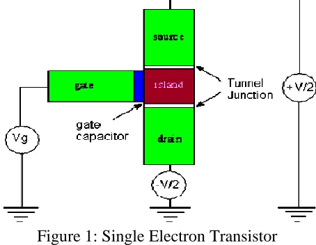
Http://www.ijetmr.com©International Journal of Engineering Technologies and Management Research [295] functionality beyond that attainable with CMOSFETs. Single-electron devices are promising as new nanoscaled devices because single-electron devices retain their scalable property and moreover, they can manage the motion of a single electron (Krishnan, 2014). Therefore, if the single-electron devices are used as ULSI elements, the ULSI will have the attributes of extremely high integration and extremely low power consumption. The utilization of single electron devices in ULSIs is expected to reduce the power consumption of ULSIs. SET is said to be the tiny transistor with tiniest power consumption.” SETs are necessary for ULSI design. Unlike FET, SET have quantum trend which is known as Tunnel effect. The organization of SETs is given in Figure 1.
Figure 1: Single Electron Transistor
In Figures 2 & 3, node1 specify source electrode, node 2 (and node 4) is island, and node 3 denoting drain electrodes.
Figure 2: Single Electron Transistor circuits with Single Island
The capacitance of island (C) is express by
C = 2πЄ0Єd (1)
Figure 3: SET circuits with Dual Island as SET is composed of two Tunnel Junctions.
In this the one island which are capatively coupled to gate electrode. The total capacitance of the island is given by:
ΣC = C1+C2+Cg (2)
Http://www.ijetmr.com©International Journal of Engineering Technologies and Management Research [296] 1.1.Principle of Single Electron Tunneling and Coulomb Blockade Effect
Size reduction goes along with a reduction of capacitances. For a plate capacitor of area L 2 at a separation L its capacitance C scales with L. As a consequence, the quantization of charge can dominate the behavior of circuits, in which tunnelling of single electrons carries the current. The tunnel junction capacitor is charged with one elementary charge by the tunnelling electron, causing a voltage buildup U=e/C, where e is the elementary charge of 1.6×10⁻¹⁹ coulomb and C the capacitance of the junction. If the capacitance is very small, the voltage buildup can be large enough to prevent another electron from tunnelling.
Figure 4: Structure of SET Showing Tunnel Junctions
Figure 5: A Tunnel Junction or Insulating Barrier
As shown in Figure 4 & 5 a tunnel junction is measured as a thin insulating hurdle between two conducting electrodes. The electrostatic energy (Ec) is given by
Ec = e^2/2C (3)
Where C is the capacitance of the island.
The suppression of electron transfer can be removed by one of these two cases:
(a) When the blockade energy is overcome by using thermal excitations at a temperature T:
T~To=Ec/K (4)
(b) When the blockade energy is overcome by using an externally applied voltage V:
V~Vt= Ec/e=e/2C (5)
Http://www.ijetmr.com©International Journal of Engineering Technologies and Management Research [297] 1.2.I-V Characteristics of SET
In Figure 6(a) shows the I-V characteristics for the symmetric junction circuit of single electron transistor where C1=C2 and R1=R2. In this situation region, the junction behaves like a resistor.
Figure 6(a): I-V characteristics of SET for Symmetric Junction
Figure 6(b): I-V Characteristics of the SET for Asymmetric Junction
The Fig. 6(b) represent the I-V characteristics for a highly asymmetric junction circuit for R1<<R2. In this case, the charge carriers, electrons enter through one junction and then run away to second junction due to the presence of high resistance.
2. Objectives of the Study
In microelectronic industry, making things smaller is the most valuable point, since smaller feature size implies higher computation power per unit area as well as lower cost.
The study has four objectives:
1) Modeling & designing of single electron transistor (SET) architectures.
2) To further reduce circuit area and power dissipation by utilizing SET’s unique Coulomb blockade oscillation characteristic.
3) To improve the reliability of SET-based circuits against background charges (BCs) by using different circuit structures.
4) Implementation of Switched Capacitor Filter using the designed SET.
3. Scope of the Study
Http://www.ijetmr.com©International Journal of Engineering Technologies and Management Research [298] circuits. But due to the limitation of MOS fabrication a new version of Filter are required which have a low power consumption, high operating speed and fast throughput.
4. Proposed Plan of Work (Methodology)
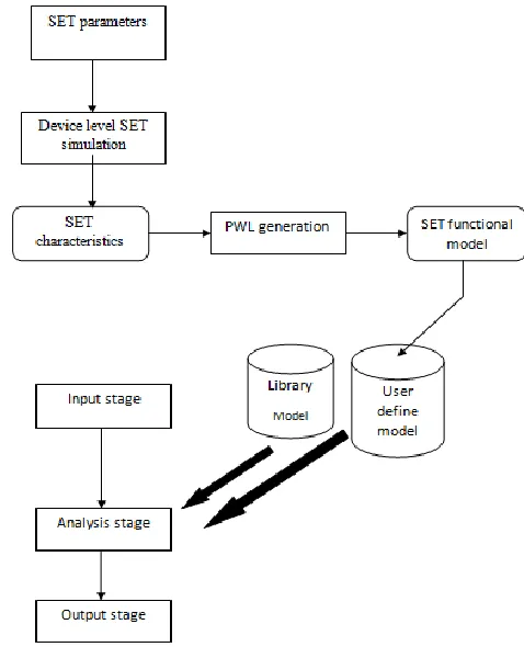
In the early days of microelectronic design, a top-to-down design flow was conceived to achieve the designs, while a bottom-up verification path was used in order to check them during every stage of design with the aim of generating a series of EDA tools. In a near future, hybrid systems composed of nanometric CMOS transistors and nano-devices, such as the SET will also need the development of a counterpart of their own design and verification paths. It is regarding the last one, that a simulation methodology is devised in order to determine their electric response. The main current obstacle when establishing a simulation strategy of hybrid systems consists in dealing with the big gap in development of both worlds, that is to say, the simulation methodology for CMOS circuits is mature even considering the new issues regarding the nanometric dimensions of the devices; while the simulation methodology for SET structures is still in its infancy. A simulation methodology for hybrid systems must cope with this circumstance while providing a reliable verification of the electric behaviour of the MOS/SET circuitry in a scheme that should be appealing for nowadays circuit designers. By considering this aspect, a particularly straightforward verification strategy for hybrid systems composed of SET devices and CMOS consists in establishing models for the SET that can be easily combined with the MOS models that are embedded in SPICE-like simulators. The methodology for simulating hybrid circuits is graphically described in the flow diagram of Figure 10. Hereafter, a step-by-step explanation of the blocks of the methodology is given.
Http://www.ijetmr.com©International Journal of Engineering Technologies and Management Research [299] Now we design the novel circuit with the help of Single Electron Transistor for microelectronics appliance and compare its characteristics with the conventional CMOS Technology.
5. Expected Outcome of the Study
A better device will be formed with the help of new technology, with high operating speed low and power consumption, which can be the future of electronics industry. A methodology for the electric simulation of SET circuits will be developed. As a result of this, a functional model for the single electron transistor will obtain and Implement Switched Capacitor Filter with the help of designed SET. The SET model can be easily coded in any hardware description language.
References
[1] Beaumont Arnaud, Dubue Christian, Beauvais Jacques, and Drouin Dominique (2009). “Room temperature Single-Electron Transistor Featuring Gate-Enhanced ON-state Current”, IEEE electron Device Letters, Vol.30, No.7.
[2] Besson, A. Perez Perez, Spiriti E, Baudot J, Claus G, Goffe M, Winter M, (2016).” From vertex detectors to inner trackers with CMOS pixel sensors” Nuclear Instruments and Methods in Physics Research Section A: Accelerators, Spectrometers, Detectors and Associated Equipment, In Press, Corrected Proof.
[3] Boubaker A. b, Troudi M. b, Sghaier Na, Souifi A, Baboux N, Kalboussi A, (2009). “Electrical characteristics and modeling of multi-island single-electron transistor using SIMON simulator”, Microelectronics Journal 40 pp.543–546.
[4] Dan Surya Shankar & Mahapatra Santanu (2010). “Analysis of Energy Quantization Effects on Single-electron Transistor Circuits”, IEEE transactions on Nanotechnology, Vol. 9, No. 1, pp 38 – 45.
[5] El-Sayed A.M., Mohamed A.A. Wahab, Mohamed G. Ahmed, (2011). Exact analytical model of single electron transistor for practical IC design Microelectronics Reliability 51 pp.733–745. [6] Goyal Shilpa, Tonk Anu, (2015). “A Review towards Single Electron Transistor (SET)”,
International Journal of Advanced Research in Computer and Communication Engineering Vol. 4, pp. 36-39 Issue 5.
[7] Jana Anindya, N Basanta Sing, Sing Jamuna K Sing and Sarkar Subir Kumar, (2013). “Design and simulation of hybrid CMOS SET circuits”, Microelectronics Reliability, Elseveier, Vol. 53, pp. 592-599, Issue 4.
[8] Krishnan Radha, (2014). “Single Electron Transistors”, International Journal of Scientific & Engineering Research, ISSN 2229-5518, Volume 5, Issue 9.
[9] Kumar Om, Kaur Manjit, (2010). “Single electron Transistor: Applications & Problems”, International Journal of VLSI Design and Communication Systems, (VLSICS), pp.24-29, Vol.1, No.4.
[10] Mittal Varun, (2013). “Basic introduction to Single Electron Transistor,” IJRASET, ISSN: 2321-9653 Vol. 1 Issue I, pp.9-13.
[11] Singh Vinay Pratap, Agrawal Arun, Singh Shyam Babu, (2012). “Analytical Discussion of Single Electron Transistor (SET),” International Journal of Soft Computing and Engineering (IJSCE), ISSN: 2231-2307, Volume-2, Issue-3, pp.502-507.
[12] Sui Bingcai, Liang Fang, Chi Yaqing, and Zhang Chao (2010). “ Nano-Reconfigurable Cells with Hybrid Circuits of single-Electron Transistors and MOSFETs”, IEEE Transactions on Electron Devices, Vol. 57 , No. 9, pp 2251 – 2257.
Http://www.ijetmr.com©International Journal of Engineering Technologies and Management Research [300] Advanced Engineering, (ISSN 2250- 2459, ISO 9001:2008 Certified Journal, Volume 3, Issue 12, pp.615-621.
[14] Parekh Rutu, Beauvais Jacques, Drouin Dominique (2014).” SET logic driving capability and its enhancement in 3-D integrated SET–CMOS circuit” Microelectronics Journal, Volume 45, Issue 8, pp. 1087-1092.
[15] Zhu Shiyang, Guo Qiang Lo (2016).” CMOS –integrated wave guide photodetectors for communications applications” Photodetectors, pp. 315-344.
*Corresponding author.