Copyright © 2014 IJECCE, All right reserved
Low Power Architecture Design of De-Blocking Filter
and Hardware Implementations in H.264/AVC
Mrs. T. Priyadarsini
Assistant Prof., ISTE Member, IAENGMember, IRED Associate Member, Dept. of Electronics & Communication Eng., V. R. S. College of Engineering & Technology, Arasur – 607107, Villupuram Dist., Tamilnadu
Mr. V. Thiyagarajan
Assistant Prof., ISTE Member, IAENGMember, Department of Electronics & Communication Engineering, V. R. S. College of Engineering & Technology, Arasur – 607107, Villupuram Dist., Tamilnadu
Ms. R. Bharadhi
Assistant Professor, ISTE Member, IAENGMember, Department of Electronics & Communication Engineering, V. R. S. College of Engineering & Technology,
Arasur – 607107, Villupuram Dist., Tamilnadu
Abstract – An adaptive in-loop de-blocking filter (DF) is standardized in H.264/AVC to reduce blocking artifacts and improve compression efficiency. This paper proposes a low power DF architecture with hybrid and intelligent edge skip filtering order. We further adopt a four-stage pipeline to boost the speed of DF process and the proposed Horizontal Edge Skip Processing Architecture (HESPA) offers an edge skip aware mechanism for filtering the horizontal edges that not only reduces power consumption but also reduces the filtering processes down to 100 clock cycles per macro block (MB). In addition, the architecture utilizes the buffers efficiently to store the temporary data without affecting the standard defined data dependency by a reasonable strategy of edge filtering order to enhance the reusability of the intermediate data. The system throughput can then be improved and the power consumption can also be reduced. Simulation results show that more than 34% of logic power measured in FPGA can be saved when the proposed HESPA is enabled. Furthermore, the proposed architecture is implemented on a 0.18μm standard cell library, which consumes 19.8K gates at a clock frequency of 200 MHz, which compares competitively with other state-of-the-art works in terms of hardware cost.
Keywords – De-Blocking Filter, H.264/AVC, Low Power Design, FPGA, Hardware Implementation.
I. INTRODUCTION
Digital video technology now plays an important role in multimedia communications. The transmission of video data requires low power, fast speed, high performance, and low cost, especially in networks with limited bandwidth. H.264/AVC is the advanced video coding standard jointly developed by the Video Coding Experts Group (VCEG) of ITU-T as Recommendation H.264 and by the Moving Picture Experts Group (MPEG) of ISO/IEC as International Standard 14496-10 (MPEG-4 part 10) Advanced Video Coding (AVC). Figure 1 shows the functional blocks of an H.264/AVC encoder. Among these outstanding coding tools, the de-blocking filter (DF) located inside the motion-compensated prediction path realized at both encoder and decoder sides of H.264/AVC, is one important tool to further increase coding efficiency and improve both objective and subjective video quality. The block-based coding structure of H.264/AVC produces artifacts known as blocking artifacts which are the unwanted discontinuities on each block boundary caused by both the quantization errors of the transform coefficients and compensation.
Copyright © 2014 IJECCE, All right reserved
II. DE-BLOCKING FILTER ALGORITHM
This section reviews the de-blocking filter algorithm employed in H.264/AVC.
A. De-blocking Filter Order
The DF uses one 4x4 block as a basic unit to process a macroblock (MB). The filtering order is to first filter along the four vertical edges from left to right and then to repeat along the horizontal edges from top to bottom while excluding the edges on the boundary of a frame. As shown in Fig. 2, the order of filtering is first from A, B, C, D, E, F, G, H first in Luma and then I, J, K, L in Cb, and finally M, N, O, P in Cr. After filtering is applied, pixels drawn in yellow may be modified on either side of a vertical or horizontal boundary in adjacent blocks, depending on the boundary strength (BS) and on the gradient of image samples across the adjacent edges. BS is an integer ranged form 0 to 4 that could be regarded as the filtering strength for updating samples. For Luma samples, if BS = 0, no filtering operation is required. If BS = 1-3, a normal filtering operation is applied to samples p0, p1, q0, and q1. If BS = 4, a stronger filtering is applied to samples p0, p1, p2, q0, q1, and q2. The BS is used to determine the appropriate strength of the filter applied to the edge.
Fig.2. Order of filtering for Luma and Chroma in one macroblock.
B. De-blocking Filter Algorithm
A group of samples from the set (p2, p1, p0, q0, q1, q2) in Fig. 2 may be filtered only if (1) is satisfied.
0 0 0 1 0 1 0 BS
p q p p q q
If any condition in (1) is false, the filtering will not be applied. The purpose of the filtering threshold criteria is to disable the filtering operations and preserve the true edge when there is a relatively large absolute difference between samples across the block boundary in the original image. The thresholds α and β increase with the average of the quantization parameters (QP) of two adjacent blocks. When QP is small, a small gradient across the boundary is likely to exist due to the features of the image (not blocking effects but real edges), and such edges should be preserved by setting α and β to be low. When QP is larger, blocking distortion is likely to be more significant, and α, β are set higher so that stronger filtering can be applied.
In H.264/AVC, the DF can be divided into two filtering process modes. One is the normal mode when BS = 1, 2, or 3, and the other is the stronger mode when BS = 4. Figure 3 summarizes and illustrates the DF algorithm for luminance samples. For chrominance edge filtering, only p0 and q0 are modified. They are filtered in the same manner as luminance.
Figure 3 classifies twelve different processing cases. In Case 0, no filtering operation is applied to the samples. Cases 1-4 (drawn in blue as a group) are conditions for normal filtering modes, and Cases 5-11 (drawn in red as a group) are conditions for stronger filtering modes. In brief, the DF adaptively filters the adjacent samples on a 4x4 block edge for both of luminance and chrominance based on the threshold conditions (α , β ), the threshold clipping variables (c0, c1), BS, QP, and the input pixel values. The implementation of DF hardware may include table look-up, pixel comparison, pixel filtering with addition, shift, pixel clipping in case of overflow and output to memories or display buffers.
Fig.3. H.264 de-blocking filter algorithm for Luma samples. Where P2, P1, P0, Q0, Q1, and Q2 are pixel
Copyright © 2014 IJECCE, All right reserved
III. PROPOSED ARCHITECTURE
A. Block Diagram of the Proposed DF Architecture
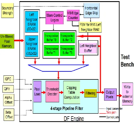
Figure 4 shows the block diagram of the proposed DF architecture where the solid line drawn in red is the sample data path, while the solid line in black indicates the control path and the dotted line is the input parameters feeding to DF Engine. A 4-stage pipeline filter inside the DF engine manages pipeline control, calculations of the threshold values, clipping functions, pixel filtering, and several conditions on each block edge based on DF algorithm. The required internal memory resources including left and upper neighbor SRAMs, transposition buffers, and left neighbor buffer are used to store pixels on the top and left boundary of MB or intermediate filtered pixels. The DF selects input data produced by these memory blocks obeying the pixel data dependency according to the MB and the order of edge filtering. The horizontal edge skip block, which is implemented by the proposed horizontal edge skip processing architecture (HESPA) mechanism intelligently skips the unnecessary filtering on the horizontal edges. The test bench including some required filtering parameters such as boundary strength, un-filtered pixels, QPC, QPY, alpha offset, beta offset, and external pseudo memory used for storing final data is designed for verifying the correctness of the proposed DF Engine across the simulator.Fig.4. Block diagram of the proposed DF architecture.
B. Proposed Pipeline Strategy and Order of Edge
Filtering
DF requires a very large memory capacity to store temporary data in the filtering process, so the order of edge filtering affects the throughput significantly [7]. The order of standardized filtering for DF is from left to right and then from top to bottom sequentially on an MB as in Fig. 5 (a). In [7], Ke Xu et al. evaluated the control hazards, structure hazards, and data hazards in their pipeline architecture. In this DF design, we proposed a 4-stage pipeline filtering architecture for 1-D edge filtering. For edge filtering, several steps need to be judged or
computed. These include the condition to be decided on each block, the calculations of the threshold values including alpha, beta, and the clipping functions, content activity check, and normal or stronger filtering.
The goal of a pipeline design is to balance the length of each pipeline stage. If the stages are perfectly balanced, the speedup from pipelining equals the number of pipeline stages. Therefore, the goal is to perform edge filtering on an MB with fluent pipeline stages and without stall cycles. Each filtered output needs 4 clock cycles to complete filtering. Thus, the total number of cycles for filtering an MB with 48 edges plus 4 cycles for initially loading the un-filtered pixels is 4 x 48 + 4 = 196 cycles. To boost the speed of the DF process, the order of filtering is rearranged in a hybrid pattern to facilitate the de-blocking of the pixels in a 4-stage pipeline fashion.
(a) Sequential filtering order.
(b) Adopted hybrid filtering order. Fig.5. Sequential and hybrid order of filtering. The numbers inside the circles and squares denote the filtering
order.
We tried many ordering schemes in the simulation to deal with the hazard issues and finally obtained the optimal hybrid order as shown in Fig. 5 (b). Although the hybrid edge order of filtering is not identical to the sequential order specified in the H.264/AVC standard, the adopted order still obeys the same rule of filtering the left edge first and the bottom edge last for each 4x4 block and hence does not affect the data dependency.
Copyright © 2014 IJECCE, All right reserved is to use as few as 4 transposition buffers to temporarily
store filtered pixels. The transposition buffer is a 4x4 array to store 16 pixels. It can be activated throughout both luma and chroma MBs by obeying the adopted filtering order meaning that the data reuse is at the unit of 4x4 basic blocks. For instance, filtering of edge6 may reuse filtered pixels of edge1.
Once filtering of edge8 is completed, the transposition buffer can be switched to the next 4x4 basic block for storing the filtered pixels of edge10. For the traditional filtering order standardized in H.264/AVC shown in Fig. 5 (a), it does not reuse data well and requires more memory or transposition buffers to store filtered pixels. For the order of edge filtering 1, 6, 10, 3, 7, 11, 17, 22, 26, 19, 23, 27, 33, 35, 41, and 43 of the different 4x4 blocks, we need transposition buffers to transpose data from the row to column to intermediately store pixels for the vertical filtering on horizontal edges. Because transposition buffers require at least 4 clock cycles to write the filtered pixels back to the current 4x4 block in our 4-stage pipeline, this filtering strategy does not proceed immediately with vertical filtering followed by horizontal filtering due to the delay of transposition buffer. By observing the filtering order carefully, we can observe that on some 4x4 blocks, the transposition buffers encounter long waiting times from edge order 5 to 20, 9 to 24, 14 to 28, and 15 to 29 to serve edge20, 24, 28, and 29, respectively. Therefore, we adopt upper neighbor SRAM to reuse the data in the design for storing the filtered results of B0, B1, B2, and B3 to be later used for edge order 20, 24, 28, and 29 as depicted in Fig. 6. Compared to Ke Xu et al. [7], we save transposition buffers for storing the upper MBs.
Fig.6. Blocks to be stored in the upper neighbor SRAM.
C. Proposed Horizontal Edge Skip Processing
Architecture
In H.264/AVC DF, filtering on some pixels can be skipped when pixel differences and threshold values satisfy some specific conditions. By exploiting this feature, we propose an intelligent filtering scheme, horizontal edge skip processing architecture (HESPA), to skip the unnecessary filtering on the horizontal edges. The proposed HESPA is applied to the horizontal edges with BS = 0 or the edges on the top boundary of a frame to
deactivate DF execution. In this way, the processing cycles of filtering can be saved and the power consumption can also be reduced.
HESPA applies to both luma and chroma MB edges. There are 48 edges to be filtered in an MB, and half of them, 24 edges, could possibly be skipped if the HESPA is enabled. To realize HESPA, functional blocks including left neighbour buffer, finite state machine (FSM) for left neighbour SRAM read/write (R/W), and some other control logic are implemented as shown in Fig. 7.
Fig.7. Proposed FSM for HESPA architecture Because the adaptive or skipped filtering steps make the left neighbor SRAM not accessed in sequential order, we need FSM and left RAM address and read/write generator to serve left neighbor SRAM adequately. Though HESPA increases some gate counts and has a small control complexity, it only consumes 10% of the total gate counts. Section IV.-B shows the results of the synthesis, which saves filtering cycles and power consumption with few cost penalties.
D. Memory Allocation and Transposition Buffer
Usage
In our DF architecture for storing temporary data during the filtering process, three types of internal memory resources are required. They are left neighbour SRAM, which stores the filtered pixels on the left boundary MB edge, upper neighbour SRAM, which provides the necessary pixels to the upper boundary of the current MB and transposition buffers, which each operates on the unit array of a 4x4 block of the current MB to store intermediate pixels. For a QCIF video with 4:2:0 format, the size of left neighbour SRAM is fixed at 32x32 bits (including 16x32 bits for luma and 16x32 bits for chroma), the size of upper neighbour SRAM is 352x32 bits (including 176x32 bits for luma and 176x32 bits for chroma), and the size of transposition buffers is 640 bits (here we count the left neighbour buffer used in HESPA as one transposition buffer).
Copyright © 2014 IJECCE, All right reserved data for our proposed HESPA mechanism. In HESPA,
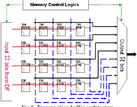
because filtering steps are skipped in the filtering process, the data flow should be managed carefully in terms of memory allocation. Otherwise, the samples are not stored for the correct space and time leading to incorrect filtering. Transposition buffers are implemented with flip flops in this design. Each transposition buffer consists of 16 samples (4x4) with a total of 128 bits or 16 bytes, which either transposes the pixels from the row to column or stores filtered data temporarily where the read/write process is accessed by memory control logic. The architecture is shown in Fig. 8.
Fig.8. Transposition buffer architecture.
The proposed order of edge filtering, together with the proposed memory organization and memory update mechanism are helpful in reducing the required memory bandwidth and maximizing the 4-stage pipeline throughput, making the filtering processes much more efficient.
IV. EXPERIMENTAL RESULTS AND
PERFORMANCE EVALUATION
A. Statistics of Boundary Strength
DF uses BS to determine the appropriate strength of the filter applied to the edge. We test three QCIF video sequences with 100 frames (Foreman, Mobile, and Stefan) for the encoding type IPPP…. The statistics of luma blocks for each BS and the percentage of BS = 0 on horizontal edges for different sequences are listed in TABLE I. We can see that BS = 0 occupies the highest proportion of distributions. Moreover, from TABLE I we can observe that BS = 0 distributes uniformly on both horizontal and vertical edges. Almost half of zero BS takes place on horizontal edges. Therefore, the percentages of filtering cycles saved for zero BS on the horizontal edges are 36.2%, 32.1%, and 30.6% for Forman, Mobile, and Stefan video sequences respectively.
Table I: BS = 0 on Horizontal Edge For Different Video Sequences
Foreman Mobile Stefan
Total BS Counts 316800 316800 316800
BS = 0 228373 202745 194781
BS = 0 on
Horizontal edge 114651 101657 96969 Cycles Saving 36.20% 32.10% 30.60% These observations support the proposal of the edge skip aware mechanism on horizontal edge filtering. The opportunities for skipping edge filtering are relatively frequent. The number of cycles for filtering an MB could be reduced from 196 down to 100 clock cycles per MB in the best case, considerably saving power consumption.
B. Synthesis Results
The proposed DF hardware architecture is implemented in Verilog RTL codes. They are verified with RTL simulations and the results are matched with the JM reference software, for the same rate-distortion performance. The proposed architecture is synthesized using a Design Compiler with a 0.18μm standard cell library. The results show that the hardware implementation consumes 19.8K gates when running at 200 MHz, where the memory elements (SRAM for neighbor and left MBs) are excluded. From the synthesis results in TABLE II, we can see that more than half of the resources (50.22%) are spent on transposition buffer, left neighbor buffer and display buffer. This is the reason we do not adopt the 2-D filtering architecture as proposed in [8]-[11].
Otherwise, a higher number of gates and larger layout areas are required in the DF hardware implementations. The 4-stage pipeline filter engine uses only approximately one-third (30.09%) of the total DF areas. To implement the HESPA intelligent mechanism, we require an additional 2.1K gates to realize the architecture. The additional resources for HESPA include the left neighbor buffer, the finite state machine for the left neighbor SRAM R/W access, and some other logic controls for edge counter awareness.
Table II: Synthesis Results for Proposed Modules
Module Gate
Counts Main Function
%
DBF_pipeline 5970.122 4-Stage pipeline
filtering function 30.09
DBF_reg_ctrl 9963.548
Transposition Buffer, Left Neighbor Buffer and Display Buffer
50.22
DBF_mem_ctrl 3907.743
Memory Control for pixel Read/ Write and order filtering Counters
19.69
Total 19841.413 100
C. Power Analysis
Copyright © 2014 IJECCE, All right reserved operation, a timing simulation of that DF hardware
implementation is first done in the test bench and the signal activities are stored in VCD files. Afterwards, these VCD files are used to estimate the power consumption of our design. Typically the power consumptions of the DF hardware implementation are divided into three main categories: signal power, logic power, and clock power. To evaluate the power consumption of the DF design, we compare with [14] because both have the same experimental conditions (Clock rate at 50 MHz and both use block SelectRAMs for internal memory). TABLE III compares the power estimation of our design with [14], which has two different hardware architectures (DBF_16x16 and DBF_4x4).
Table III: Power Consumption Estimation Comparisons With [14]
Category [14] DBF_4x4
[14] DBF_16x16
Proposed Reduction Clock 56.37Mw 50.36mW 46.63mW 3.73mW Logic 145.65mW 52.47mW 13.90mW 38.57mW Signal 83.56mW 79.39mW 42.04mW 37.35mW Total 285.58mW 182.22mW 102.57mW 79.65mW
As shown in TABLE III, we can observe that the proposed DF hardware consumes less power than [14] in all categories. Moreover, the proposed hardware has a 38.57mW power reduction in logic compared with the DBF_16x16 hardware [14], which is the greatest reduction among the three categories. This is because fewer computation cycles are used in the proposed hardware. The differences in internal memory resources and hardware performance comparisons between the proposed DF architecture and [14] are listed in TABLE IV and TABLE V respectively. From TABLE IV we see that [14] utilized left neighbor memory instead of buffers to store intermediate data. This causes more power consumption when utilizing on-chip SRAM instead of using the buffers [13]. Also, from TABLE V, 5248 or 5376 processing cycles is required to filter an MB in [14]. In this scheme, only 100-196 cycles/MB is required. A possible reason is that [14] adopted an 8-bit data bus to access each pixel while our design utilized a 32-bit wide data bus to access 4 pixels each time.
Table IV:Internal Memory Comparisons with [14] Memory Required [14](bits) Proposed (bits) Left Neighboring
Memory
384x8=3072 32x32=1024 Upper Neighboring
Memory (for QCIF)
1408x8=11264 352x32=11264 Transposition Buffers
and Left Neighbor buffer
0 5x128=640
Table V: Hardware Performance Comparisons with [14]
HW Comparison [14] Proposed
Gate Counts (without internal buffers)
5.3K 9.9K
Technology 0.18μ 0.18μ
Processing cycles/MB 5248/5376 100-196
D. Power Analysis of HESPA
We now evaluate the power saving for the proposed HESPA approach. Table VI lists three categories of power estimation and compares the power reduction between HESPA in the on state and HESPA in the off state. The proposed HESPA can save up to one-third (34%) of total power consumption in logic and signal processing and thus can speed up DF processing significantly. This result matches with Section IV.-A, which describes that BS = 0 on horizontal edges is about one-third of total BS counts. Therefore, roughly one-third of the total number of processing cycles can be saved when the BS is zero on horizontal edges or the edges are on the top boundary. The number of cycles saved corresponds to power saving in the simulation because we use enable bit to stop DF clock or to halt DF processing when filtering is completed. However, no reduction in clock power
Table VI: Power Comparisons between HESPA On/Off Sequence 100 frames of Forman QCIF Category HESPA OFF HESPA ON Reduction
Clock 46.63mW 46.63mW 0
Logic 21.10mW 13.90mW 34.12%
Signal 63.80mW 42.04mW 34.11%
Whole FPGA 624.36mW 579.08mW 7.25%
E. Performance Comparisons
This section compares our DF hardware performance with various state-of-the-art designs. The design requires fewer transposition buffers and fewer gate counts than [7], which used a similar design approach to this one (pipeline stage and 1-D filtering architecture). Although this design requires more processing cycles than in Tobajas et al. [8], we can lower the gate count and achieve lower transposition buffer usage. That is because in [8], a double filter with two identical filtering units was proposed as opposed to our 1-D filtering strategy. Moreover, the proposed HESPA, an intelligent edge skip processing approach, can achieve as few as 100 cycles per MB in the best case, which even outperforms the 2-D architecture in [8] (110 cycles). The design consumes 19.8K gates at a clock frequency of 200 MHz in a 0.18μm standard cell library. The hardware cost of the proposed scheme is very competitive compared with other state-of-the-art literatures using 1-D filtering architecture.
V. CONCLUSION
Copyright © 2014 IJECCE, All right reserved realize the proposed HESPA method. The hardware of our
de-blocking filter architecture can adaptively achieve 100~196 cycles per MB throughput for H.264/AVC real time decoding. The architecture is designed in Verilog and implemented by 0.18μm CMOS technology. The gate count is only 19.8K when synthesized at 200 MHz, excluding the memory cost. The system throughput can easily support 1080HD video format at 30 fps with 70MHz clock frequency for low power and high definition video applications.
REFERENCES
[1] ISO/IEC ITU-T Rec. H264: Advanced Video Coding for GenericAudiovisual Services, Joint Video Team (JVT) of ISO-IEC MPEG & ITU-T VCEG, Int. Standard, May 2003. [2] P. List, A. Joch, J. Lainema, G. Bjontegaard, and M.
Karczewicz“Adaptive deblcoking filter,” IEEE Trans. Circuits Syst. Video Technol.,vol. 13, no.7, pp. 614-619, July 2003. [3] J. Rabaey, “Low-Power Silicon Architectures for Wireless
Communication,” Asia and South Pacific Design Automation Conference, 2000, pp.379-380.
[4] Y. W. Huang, T. W. Chen, B. Y. Hsieh, T. C. Wang, T. H. Chang, and L.G. Chen, “Architecture design for de-blocking filter in H.264/JVT/AVC,” in Proc. IEEE Int. Conf. Multimedia Expo., July2003, vol. 1, pp.693-696.
[5] G. Khurana, A. A. Kassim, T. P. Chua, and M. B. Mi, “A pipelined hardware implementation of in-loop de-blocking filter in H.264/AVC,”IEEE Trans. Consum. Electron., vol. 52, no. 2, pp. 536-540, May 2006.
[6] Q. Chen, W. Zheng, J. Fang, K. Luo, B. Shi, M. Zhang, and X. Zhang,“A pipelined hardware architecture of de-blocking filter in H.264/AVC,”Third International Conference on Communications and Networking inChina, China Com 2008, pp. 815 -819.
[7] K. Xu and C. S. Choy, “A Five-Stage Pipeline, 204 Cycles/MB, Single-Port SRAM Based De-blocking Filter for H.264/AVC,” IEEE Trans.Circuits Syst. Video Tech., vol. 18, no. 3, pp.363-374, Mar. 2008.
[8] F. Tobajas, G. M. Callico, P.A. Perez, V. de Armas, and R. Sarmiento,“An Efficient Double-Filter Hardware Architecture for H.264/AVC De-blocking Filtering,” IEEE Trans. Consum. Electron., vol. 54, no. 1,Feb. 2008.
[9] Y. C. Lin and Y. L. Lin, “A Two-Result-per-Cycle De-blocking Filter Architecture for QFHD H.264/AVC Decoder,” IEEE Trans. VLSI Syst.,vol. 17, no. 6, June 2009.
[10] H. Loukil, A. B. Atitallah, and N. Masmoudi, “Hardware architecture forH.264/AVC de-blocking filter algorithm,” 6th International Multi-Conference on Systems, Signals and Devices, 2009, pp. 1-6.
[11] T. H. Tsai and Y. N. Pan, “High efficient H.264/AVC de-blocking filter architecture for real-time QFHD,” IEEE Trans. Consum. Electron., vol.55, no. 4, pp. 2248-2256, Nov. 2009. [12] S. Y. Shih, C. R. Chang, and Y. L. Lin, “An AMBA-compliant
de-blocking filter IP for H.264/AVC,” in Proc. IEEE International Symposium on Circuits and Systems, May 2005, vol. 5, pp. 4529-4532.
[13] N. T. Ta, J. Youn, H. Kim, J. Choi, and S. Han, “Low-power high throughput de-blocking filter architecture for H.264/AVC,” International Conference on Electronic Computer Technology, 2009.
[14] M. Parlak and I. Hamzaoglu, “Low power H.264 de-blocking filter hardware implementations,” IEEE Trans. Consum. Electron., vol. 54, no. 2, pp. 808-816, May 2008.
[15] Xilinx Inc., “XPower Tutorial: FPGA Design,” XPower (v1.3), July 15,2002, 1-800-255-7778.
[16] B. Sheng, W. Gao, and D. Yu, “An implemented architecture of de-blocking filter for H.264/AVC,” in Proc. Int. Conf. Image Process.,Oct. 2004, vol. 1, pp. 24-27.
[17] C. C. Cheng, T. S. Chang, and K. B. Lee, “An in-place architecture for the de-blocking filter in H.264/AVC,” IEEE Trans. Circuits Syst. II, vol.53, no. 7, pp. 530-534, Jul. 2006.
[18] T. M. Liu, W. P. Lee, T. A. Lin, and C. Y. Lee, “A memory-efficient de-blocking filter for H.264/AVC video coding,” in Proc. IEEE International Symposium on Circuits and Systems, May 2005, vol. 3, pp.2140-2143.
[19] K. Y. Min and J. W. Chong, “A memory and performance optimize architecture of de-blocking filter in H.264/AVC,” in Proc. Int. Conf.Multimedia Ubiquitous Eng., Apr. 2007, pp. 220-225.
AUTHOR’S PROFILE
Priyadarsini.T
is currently working as a Assistant Professor in Department of Electronics and Communication Engineering, V.R.S. College of Engineering & Technology, Arasur-607107, Villupuram District, Tamilnadu, INDIA. She is an ISTE Member, IAENG Member, the IRED Associate Member. She received M.E. degree in 2011, B.E. degree in 2007 from Anna University, Chennai. She has published widely several topics in National & International Conferences and also in International Journals.
Thiyagarajan.V
is currently working as a Assistant Professor in Department of Electronics and Communication Engineering, V.R.S. College of Engineering & Technology, Arasur-607107, Villupuram District, Tamilnadu, INDIA. He is an ISTE Member, IAENG Member. He received M.E. degree in 2011 from Sathyabama University, B.E. degree in 2007 from Madras University, Chennai. He has published widely several topics in National & International Conferences and also in International Journals.
![Table III: Power Consumption Estimation Comparisons With [14] [14]](https://thumb-us.123doks.com/thumbv2/123dok_us/8787330.1764664/6.595.50.297.262.339/table-iii-power-consumption-estimation-comparisons.webp)
