An FSK Demodulator Design for RF Wireless
Sensor Applications Using Zigbee Protocol
Abstract—In this paper, transistor-level simulations of a detector called “cross-differentiate-multiplier demodulator (CDM)” are presented. This detector, which uses three blocks (a differentiator, a multiplier and a subtractor), is able to demodulate a received bit sequence, that was transmitted using a frequency-shift keying modulation scheme, with a bit rate equal to 20kbps. The application of this detector will be in a wireless sensor receiver operating in the 863-870MHz ISM band. In this sensor, a frequency hopping spread spectrum is used as modulation technology and Zigbee (IEEE 802.15.4) as the communication protocol. Design is performed using 0.35µm CMOS technology and a 3V supply. A comparison between the performances of different architectures studied, mainly in terms of BER, is presented at the end of this document.
Index Terms—cross-differentiate-multiplier demodulator, direct conversion receiver, zigbee protocol, wireless communication, BER simulations, 0.35µm CMOS technology
I. INTRODUCTION
The market for wireless connectivity has been growing rapidly in the past few years. A number of standards have been developed to satisfy the requirements of various parts of this market. These systems have unique characteristics and engineers will face new implementation challenges. The most severe design constraint is the limited amount of energy available for a wireless node. Beside this challenge, low cost and small size are two important features for a product that wants to reach the largest part of the consumer market.
The FSK demodulators are simple to implement and they provide a major advantage in terms of energy consumption on the transmitter’s side, due to the possibility of using a non linear amplification of the intrinsic constant envelope modulation format.
Bluetooth and Zigbee are the standards most likely to be used in wireless sensor networks. A performance comparison of these two standards has to adopt the Zigbee for our application. Its very low power consumption and low production costs make it an ideal candidate for connecting devices like sensors. Made in 2003, Zigbee is a protocol that provides simple and powerful error correction and the ability to change the frequency to avoid interference [1]. For the applications
Manuscript received January 21, 2014; revised June 10, 2014.
of wireless sensor network at low power and batteries, the maximum range was set at 50m and the maximum power transmitted was set at 0dBm.
In this paper, we present the receiver architecture adopted for our application. Then, Binary FSK Cross-differentiate-multiplier (CDM) demodulator blocks are explained and a transistor-level simulation is detailed. Finally, simulation results and performances comparison are presented to conclude this paper.
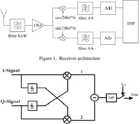
II. RECEIVER ARCHITECTURE
There are various architectures for RF receiving systems. They are characterized by the arrangement and the number of blocks they use, but they must meet the technical parameters set by the standard. A high level of integration, flexibility and low power consumption are the main criteria for selecting architecture. Zigbee specifications structures promote zero IF or low IF (IF<10MHz) due to the extremely short preamble access code. Also the hardware minimization can be achieved by using a direct conversion (zero-IF) architecture, which eliminates the image-reject filter and other IF components, enabling a monolithic transceiver [2].
A Binary Frequency-Shift Keying (BFSK) modulation was selected because it is well suited for direct conversion architecture [3]. The block diagram of the receiver for a wireless sensor node is shown in Fig. 1.
Figure 1. Receiver architecture
Figure 2. Cross-Differentiate-Multiplier demodulator
Amel Neifar, Hatem Trabelsi, and Mohamed Masmoudi
III. DESIGN OF THE BINARY FSKCROSS -DIFFERENTIATE MULTIPLIER DEMODULATOR
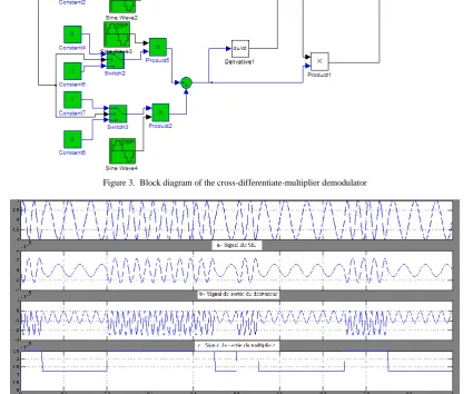
The principle of the demodulator is to extract a cosine frequency from (I channel) and a sine wave from (Q channel) using the property (sin2α+cos2α) = 1. The block diagram is described in Fig. 2.
Indeed, after derivation and a cross multiplication of the two channels I and Q, the following (1) and (2) are obtained:
( ) ( ) ( ) ( ) (1)
( ) ( ) ( ) ( ) (2)
Then;
( ) ( ) ( )
( ) ( ) ( ) (3)
This gives the frequency of the transmitted signal to nearly a constant as in (3) and thus, the frequencies allocated to the digital 0 and 1 may be distinguished [4]. Fig. 3 shows the block diagram of the demodulator simulated in Simulink-Matlab.
Figure 3. Block diagram of the cross-differentiate-multiplier demodulator
Figure 4. Output signals of each block of BFSK demodulator
The BFSK signal shown below in Fig. 4a attacks the demodulator which will first make a derivation of both I and Q channels (I and Q are two sinusoidal signals same
differentiation and they give the signal of Fig. 4c. Finally, after subtracting the output signals of the multipliers there should be a signal identical to the transmitted one but shifted up as shown in Fig. 4d. Indeed, the level 1 will be represented by 2πf1 and level 0 by 2πf2. For example: if we take f1=40KHz and f2=20KHz then the demodulator output gives a value of 251×103 for the bit “1” transmitted and 125×103 for the bit “0” transmitted.
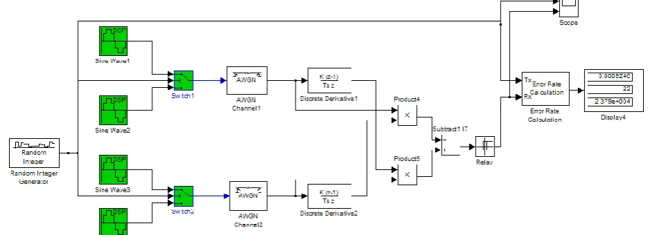
To determine the performance of the detector, a White Gaussian Channel Noise was added to the circuit, as shown in Fig. 5, the parameters of the input power has been set at 0dBm, and the number of bits per symbol at 2000 bits/symbol to meet the needs of the application. The received sequence is compared to the transmitted one in Fig. 6 and the bit error rate was calculated by varying the Eb/N0.
Figure 5. Simulating circuit for calculating the bit error rate
Figure. 6. Transmitted and received signals
By plotting the values obtained of the bit error rate as a function of Eb/N0 in dB; the curve of Fig. 7 is obtained.
We note that for an error rate of 103, only 11dB of signal_to_noise ratio is needed which satisfies the requirements of the application.
Figure 7. BER plot versus EbtoNo (dB), using CDM demodulator
Figure 8. BFSK demodulator diagram designed with ADS
IV. TRANSISTOR-LEVEL SIMULATIONS
0 2 4 6 8 10 12 14
10-5 10-4 10-3 10-2 10-1 100
Eb/N0
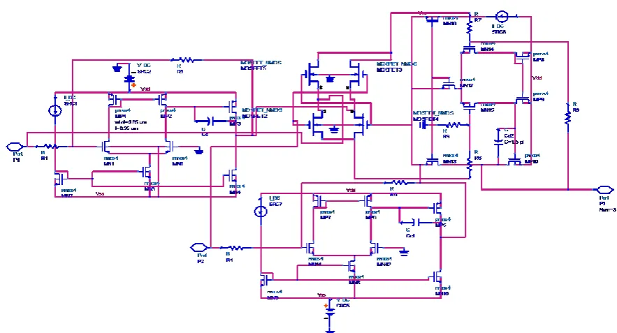
The performances of the CDM detector have been simulated using ADS; Fig. 8 shows the block diagram of the proposed detector. It is composed of differentiators, multipliers and subtractors. The architecture of each component is detailed below.
A. The Differentiator
The first block of the demodulator is the differentiator [5]. Fig. 9 shows its internal circuit.
Figure 9. Internal architecture of the differentiator
Calculation is performed for the Q channel:
( ) ( )
The differentiator is based on operational amplifier; the output signal is given by the following (4):
F =
= ( ) (4)
So for R = 100ohm and C = 100pF we obtain: For f1 = 40KHz: F = -2.51×10⁻³ sin(2πf1t) For f2 = 20KHz: F = -1.25×10⁻³ sin(2πf2t)
The following Fig.10 shows the simulation results of the differentiator.
Figure 10. Input and output signals of the differentiator
B. The Multiplier
The second block is the multiplier. This is a circuit to which two input voltages V1 and V2 are applied, thus will be recovered an output voltage equal to the product of the two input voltages. If V1 and V2 are two sinusoidal signals of frequency f1 and f2, in the output signal we don’t only find the components of input frequencies but also the frequencies f1+f2 and |f1-f2| whose amplitudes are proportional to the product of the amplitudes of the input signals.
There are various architectures of multipliers. They can be designed on the basis of transistors or diodes. In all cases, it is the non-linearity of the voltage control current output which is used to obtain the desired effect. Among these architectures, we chose “the multiplier FET rings” [6]. The principle of multiplication is ensured by the mixture that has a frequency mixer. Its diagram is given in Fig. 11.
Figure 11. Diagram of a multiplier ring FET
This mixer is double balanced, consisting of 4 FET transistors, whose characteristics must be as close as possible, and 3 Baluns (RF, IF and LO). During the positive half cycle of the LO signal, both transistors are conducting and the two others are blocked which means that the RF signal reaches the IF Balun through the conducting transistors. During the negative half period of the LO signal, the conducting transistors become blocked and vice versa. The result is reversing the polarity of the RF signal which will reach the IF balun. The frequency at which the FETs are closed or blocked is determined by the frequency of the LO signal. This is mathematically equivalent to a multiplication of the RF and LO signals
which causes the generation of the sum and difference frequency IF port. We used this topology in the design of our demodulator to calculate the square of the output signals of the differentiators.
As for the I and Q channels:
Y(t) = ×I(t) =-2πf sin(2πft)×sin(2πft) = -2πf sin2(2πft)
X(t) = ×Q(t)=2πf cos(2πft)×cos(2πft) = 2πf cos2(2πft)
Fig. 12 shows the architecture of the achieved multiplier.
The simulation result of the multiplier provides the signals X and Y in mV shown in Fig. 13.
Figure 13. Output signals of the multipliers
C. The Subtractor
The last block in our demodulator is the subtractor. There are several architectures that can play this role in our design. A comparison of simulations [5] and [7] allowed us to choose the topology of Fig. 14.
Figure 14. Internal architecture of the subtractor
For the calculation of the subtraction; we know that for an architecture based on operational amplifier [8], the equation of the output signal of the subtractor is (5):
( ) ( + ) (5)
Choosing R1=R3 and R2=R4, (5) becomes (6):
( ) (6)
For f1 = 40 KHz:
In1= -2.51×10⁻³ sin2(2πf1t) In2= 2.51×10⁻³ cos2(2πf1t)
For f2 =20KHz:
In1 = -1.25×10⁻³ sin2(2πf2t) In2 = 1.25×10⁻³ cos2(2πf2t)
In our case: R1= 10Kohm and R2 = 1Kohm;
For f1:
Vout=0.1×2.51×10-3[cos2(2πf2t)+sin2(2πf2t)]=2.51×10⁻⁶
For f2:
Vout=0.1×1.25×10-3[cos2(2πf2t)+sin2(2πf2t)]=1.25×10⁻⁶
In Fig. 15, the output signal of the subtractor, which is the last block of our demodulator, is compared to the signal above, which is the transmitted sequence before modulation. We note that the signals are identical but the received one is shifted up due to changes in the amplitude and it also presents corrugations caused by noise from all blocks of the receiver. Adding a block “Integrate and Dump” will eliminate these imperfections.
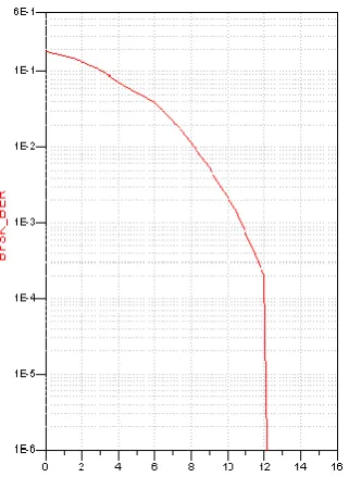
V. SIMULATION RESULTS AND PERFORMANCES COMPARISON
Fig. 16 shows the bit error rate as a function of signal to noise ratio for our simulated system. We note that to achieve 10-3 of BER we need only 10.4dB of Eb/N0. This shows that this demodulator is more efficient for our receiver than other demodulators which are already studied like the zero crossing BFSK demodulator (the BER curve function of (Eb/N0) is presented in Fig. 17) [9], correlating BFSK detector and Arctangent differentiated demodulator [2].
Figure 16. BER versus EbtoNo of our system
Figure 17. BER plot versus EbtoNo (dB) using the zero crossing demodulator
VI. CONCLUSION
In this study, we focused mainly on designing the different blocks of a Cross-differentiate-multiplier (CDM) BFSK demodulator. The designed architecture was first simulated under Matlab using Simulink blocks, then under ADS environment using 0. 5μm technology. Comparing with other demodulators at a BER of 10-3, the detector has shown very interesting results in terms of Signal_to_noise ratio performance (EbtoNo=10.4dB) and sensitivity which reached -116dBm.
As a work perspective, we aim to make co-simulations with the analog receiver to assess the noise and consider achieving an integrated circuit of the entire transceiver.
REFERENCES
[1] ECC REP037, “Compatibility of planned SRD (short range devices) applications with currently existing radio communication in the frequency band 863-870MHz applications,” Technical Report: Electronic Communications Committee (ECC) within the European Conference of Postal and Telecommunications Administrations (CEPT), Granada, Feb. 2004.
[2] H. Trabelsi, G. Bouzid, F. Derbel, and M. Masmoudi, “A 86 -870MHz spread-spectrum FSK transceiver design for wireless sensor,” Microelectronics Journal, vol. 41, no. 8, pp. 465-473, Aug. 2010.
[5] F. P. Cortes and S. Bampi, “Miller OTA design using a design methodology based on the gm/id and early-voltage characteristics: Design considerations and experimental results,” Federal University of Rio Grande do Sul (UFRGS), Informatics Institute, 2006.
[6] M. T. Terrovitis and R. G. Meyer, “Noise in current-commutating CMOS mixers,” IEEE Journal of Solid-State Circuits, vol. 34, no. 6, Jun. 1999.
[7] E. M. Spinelli and M. A. Mayosky, “Un amplificador operacional equilibrado,” IEEE Latin America Transactions, vol. 5, no. 8, Dec. 2007.
[8] (2013). Electronique radioamateur. [Online]. Available: www.electronique-radioamateur.fr
[9] A. Neifar, H. Trabelsi, G. Bouzid, M. Masmoudi, “Design of a zero crossing BFSK demodulator for a wireless sensor,” in Proc. 7th International Conference on Desig and Technology of
Integrated Systems in Nanoscale Era (DTIS), May 2012, pp.1-5.
Amel Neifar is a Ph.D student in the
Micro-Electro Thermals Systems Laboratory in the National School of engineers of Sfax. She was born in Sfax, Tunisia, in 1986 where she studied electrical engineering and received the engineer degree in 2010 and the Master degree in Electronics in 2011 both from the National School of engineers of Sfax. Tunisia.
Hatem Trabelsi was born in Sfax, Tunisia in
1969. He received the engineering degree in electrical engineering from the National School of Engineers of Tunis in 1993, the aggregation degree in 2001 and Ph.D. in electrical engineering from the National School of Engineers of Sfax in 2009. His doctoral research was mainly focused on design and implementation of ultra low power transceivers for Wireless Sensor Network. He is currently an Assistant Professor at the Electrical Engineering Department of the National School of Engineers of Sfax. He is a member of the research laboratory METS LAB ENIS, where he is working in the field of analog and RF circuit design for ultra-wideband systems. His research interests are single-chip CMOS transceivers, RF front-ends, Ultra wideband analog circuit design.
Mohamed Masmoudi was born in Sfax,
Tunisia, in 1961. He received the Engineer degree in electrical Engineering from the National Engineers School of Sfax, Sfax, Tunisia in 1985 and the PhD degree in Microelectronics from the Laboratory of Computer Sciences, Robotics and Microelectronics of Montpellier, Montpellier, France in 1989. From 1989 to 1994, he was an Associate Professor with the National [3] Specification of the Zigbee System, version 1.1, Feb. 2001. [4] E. Lopelli, J. D. Van Der Tang, and A. H. M. Van Roermund,FSK
Demodulator Topologies for Ultra-low Power Wireless
Engineers School of Monastir, Monastir, Tunisia. Since 1995, he has been with the National Engineers School of Sfax, Sfax, Tunisia, where, since 1999, he has been a Professor engaged in developing Microelectronics in the engineering program of the university, and where he is also the Head of the Laboratory Micro-Electro Thermals