Soft Lithographic Patterned Architectures in Dye Sensitized Solar Cells
Myoung-Ryul Ok
“A dissertation submitted to the faculty of the University of North Carolina at Chapel Hill in partial fulfillment of the requirements for the degree of Doctorate of Philosophy
in the Curriculum in Applied Sciences and Engineering.”
Chapel Hill 2013
Approved by
Edward T. Samulski Alfred Kleinhammes John M. Papanikolas Rene Lopez
ABSTRACT
MYOUNG-RYUL OK: Soft Lithographic Patterned Architectures in Dye Sensitized Solar Cells
(Under the direction of Edward Samulski)
Arrays of periodic surface features were patterned on mesoporous Nb2O5 and TiO2
films by soft-lithographic techniques to construct photonic crystal (PC) structures on the back
side of the oxide. The patterned oxide films were integrated into dye-sensitized solar cells
(DSSCs) and their performance was evaluated relative to flat (unpatterned) counterparts. The
PC structure on niobium oxide surfaces caused large changes in optical characteristics,
particularly in the blue wavelength regime. The incident photon-to-current conversion
efficiency (IPCE) of patterned niobium oxide anodes exhibited a relative enhancement over
the entire wavelength range corresponding to the higher absorption in optical measurements.
However, the effect of surface PC structures on the optical response of the TiO2 is different
from that of the Nb2O5 photoanode. The enhancement of light harvesting efficiency (LHE) is
not obviously due to the higher thickness and larger dye loading than Nb2O5 films. However,
patterned TiO2 samples exhibited higher global efficiency than the flat reference, although
there was no notable change in LHE. It was hypothesized that surface PC structures changed
the de-trapping rate from trap states based on the simulated reflection behavior near the
surface of the PC structure, and that in turn, enhances charge collection efficiency.
A cubic array of rectangular ITO posts (556.5µm, 10µm period) were fabricated on
mesoporous TiO2 film and the transparent conductive oxide (TCO) layer in an effort to
enhance charge collection in the DSSCs. In spite of the decrease in optical transmission due
to the tall ITO structures, DSSCs with patterned ITO exhibited increased photocurrent by
12~18% to the reference DSSCs with identical volume of sensitized TiO2. However, DSSCs
with patterned ITO substructures showed deterioration in the open circuit voltage (Voc), fill factor, and global efficiency. Electrochemical impedance spectroscopy (EIS) showed that
DSSCs with patterned ITO exhibited faster recombination rates leading to the decline in Voc,, fill factor, and global efficiency. We conclude that a barrier coating to suppress back electron
transfer to the electrolyte should be conformally applied in order to take full advantage of the
ACKNOWLEDGEMENTS
I would like to express my appreciation to those numerous people who helped me to
complete this work in many aspects.
Most of all, I owe the greatest thanks and praise to my advisor, Dr. Edward T.
Samulski. He’s been not only the perfect teacher in science with his ingenious ideas and
stimuli, but a real mentor who always cares for my whole life in Chapel Hill. His intelligence
guided me to the right direction and his tolerance and warmth waited till I could find a
breakthrough myself whenever I encountered a wall in science. Also, my whole family
deeply thanks him and Mrs. Samulski for their encouragement and consideration.
I also want to express my special thanks to Prof. Rene Lopez for his support and
discussion. My research got nurtured by his stimulating discussions and encouragement.
Without his support, I would have lost my way in optics and could not have overcome many
challenges in this work. I would like thank to Prof. Sheiko for his discussions and care in my
beginning days and help as a committee member. I also express my thanks to Prof.
Papanikolas for his help as a committee member and his inspiration to the ITO works. And I
want to thank Prof. Kleinhammes and Prof. Wu for their help as the committee member for
my defense and prelim.
There are many I would like to express my gratitude for their support and discussion.
this group. His help is not limited only to the science, but includes timely lessons and advice
to the life in Chapel Hill. Also, for my research, I cannot express my thanks too much to the
help of Kyle, Rudy, and Leila. They taught me how to use lots of instruments and shared
their ideas and time for discussion. Also, as my topics cover optics and PFPE, I owe much to
Lopez group (Eugene, Emily, Cary, Yuki, Yingchi, Tim, and John) and Prof. DeSimone and
his group (especially Chris and Charlie). I also want to express my thanks to Hanlin for her
help and discussion. The CHANL also supported me much, and I want to thank Carrie, Amar,
Bob, and Wallace. I also want to express my appreciation to the UNC EFRC for the research
funding and many chances of seminar and useful discussions: I appreciate Prof. Meyer, Dr.
Hoertz, Catherine, Ralph, and many other people in the center.
I also express my gratitude to the CASE and the administrative people to help me to
work in the UNC Chapel Hill. I want to thank Carolyn Newman for her help on my first day
in the office, Prof. Qin for his concern for the students during the first two semesters, and
Prof. Washburn for his support as an associate chair of Applied Science. Also, I want to
thank Duane for his help and warm advice as the physics lab director.
There are many friends who lubricated my life in Chapel Hill. I want to thank Tony
for his warm heart and encouragement. I really enjoyed my years in the Samulski lab and
want to express my thanks to the members, Yongchao, Walter, Agata, Craig, Mukti, Abay,
and the last student of this group, Leah. Also, there are many Korean friends who shared
their ideas, heart, and energy when I need help, advice, and/or relief. Most of all, I want to
express my special appreciation to Dr. Sangwook Wu for his mentoring whenever I got
depressed by the hardship as a student or a father. Also, I would like to thank Dr. Jinwoo
Changjun Lee, and Prof. Soo-Hyoung Lee. I also want to express my gratitude to Seung Hun
for his friendship, and finally, Dr. Ahyeon Koh, and Soo Yeon Sim for their help, discussion,
and shared memories in Chapel Hill. Also, I want to encourage Yejee Han who is about to
start her life in the UNC Chapel Hill.
There are also many people I want to express my gratitude in Korea. I would like to
express my special thanks to Dr. Kyung Tae Hong, who helped me to start my professional
career as a scientist and taught me a lot of virtues a scientist should have. I also want to thank
Prof. Dongil Kwon for his instruction that helped me to build a strong foundation as a
professional. I also want to express my gratitude to Dr. Seunghee Han and Dr. Eric Fluery for
their help in research and the application process. And I would like to thank Dr. Jin-Yoo Suh
for his overall contribution to my career and life. I want to express my thanks to Dr.
HyunKwang Seok for his support and concern to my future direction. And I feel really sorry
there are too many scientists and staffs to acknowledge here, especially in KIST, but the
pages are limited: I want to express my thanks to all of them and apologize not to be able to
write down all of their names.
However, I could not complete my requirements without the encouragement and
support from my family. First of all, my mother is the most influential person of all. From my
childhood, she always raised me in a more difficult but powerful way, by showing me
commitment, tolerance, and honor, rather than referring those virtues. I want to express my
gratitude and love to her. I feel sorry my father cannot see me become a Ph.D, but his love
remained in me, and I feel his love to me was actually much bigger than I felt in the past, as I
become a father myself. Also, I want to express my special thanks to my sisters for their
brothers-in-law for their support and concerns like the real ‘brothers’, and nephews and
nieces, Sehoon, Sanghyun, Se-in, and Soyeon.
And I cannot express my thanks too much to my father-in-law and mother-in-law:
they have always regarded me and my wife’s decisions, encouraged us, and never saved their
support and blessing. Moreover, especially when my two kids were born, without their
special care, I could not have reconciled myself to a father. I also thank my sister-in-law and
her family for their encouragement and concern.
But, the greatest contribution to my Ph.D was from my wife, Eun Young. Although
she encountered the first hardship in her life as a wife of a foreign student and had to struggle
to overcome loneliness, she always encouraged and supported me by her brightness and
sacrifice, as a good wife and mother. I would express my special appreciation and love to her,
beyond the limits of language. Also, I want to express my love to my sons, Jino and Sean,
TABLE OF CONTENTS
LIST OF TABLES……….…xiii
LIST OF FIGURES………..…..xiv
LIST OF ABBREVIATIONS AND SYMBOLS……….xviii
1. Literature Review of and Introduction to Soft-lithography and Dye-Sensitized Solar Cells...1
1.1 Introduction to soft-lithography………..….1
1.1.1 Photolithography………..…….2
1.1.2 Soft-lithography……….4
1.2 Dye-sensitized solar cells (DSSCs)……….6
1.2.1 Basic principles and terms of DSSCs………....7
1.2.2 Issues for the enhancement of the power conversion efficiency………..11
1.2.3 Photonic crystal (PC) structures………...…14
1.3 Scope of thesis………18
1.4 References………21
2. Surface Patterning of Mesoporous Niobium Oxide Films for Solar Energy Conversion…27 2.1 Introduction………27
2.2 Experimental………...…29
2.2.1 Preparation of the niobium oxide paste via sol-gel synthesis………...29
2.2.2 Preparation of the patterned PFPE mold………..29
2.2.4 Characterization of the nanostructure of the patterned niobium oxide………31
2.2.5 Evaluation of the solar energy conversion performances……….31
2.3 Results and Discussion………...34
2.3.1 Morphological analysis of the patterned niobium oxide films……….…34
2.3.2 Crystallographic characterization of the patterned niobium oxide films….…36 2.3.3 Optical properties of the patterned niobium oxide films………..38
2.3.4 Photoelectrochemical solar energy conversion by IPCE measurement……...42
2.4 Conclusions……….45
2.5 References………...46
3. Surface Patterning on Mesoporous Titania for Dye-Sensitized Solar Cells………49
3.1 Introduction………49
3.2 Experimental Section………..51
3.2.1 Materials………...51
3.2.2 Preparation of patterned PFPE molds………...51
3.2.3 Preparation of patterned electrodes………..52
3.2.4 Analytical instrumentation………...53
3.2.5 Sensitization of electrodes………54
3.2.6 DSSC preparation and photochemical measurements………..…54
3.3 Results and Discussion………...55
3.3.1 Analysis of the surface morphology and patterns………55
3.3.2 Optical characterization of the sensitized TiO2 films……….…..56
3.3.3 Characterization of photoelectrochemical solar energy conversion………….63
3.3.5 Alternative approaches to resolve discrepancies………..74
3.4 Conclusions………...….79
3.5 References………..………...….81
4. Patterned ITO Substrate for Enhanced Electron Collection in the Dye-Sensitized Solar Cells………84
4.1 Introduction………....84
4.2 Experimental………..87
4.2.1 Fabrication of the ITO paste………...….87
4.2.2 Fabrication of patterned PFPE mold for soft-lithography………87
4.2.3 Preparation of the anodes on top of the patterned TCO substructures……....88
4.2.4 Assembly of the DSSCs………..89
4.2.5 Characterization of the DSSC structure and photoelectrochemical Performances………....90
4.3 Results and Discussion………..90
4.3.1 Structural analysis of the DSSC with patterned ITO sublayer…………..…..91
4.3.2 Optical Characterization……….92
4.3.3 Resistivity of the ITO……….………94
4.3.4 Photoelectrochemical characterization of the DSSCs………97
4.4 Conclusions……….……..105
4.5 References……….107
5. General Conclusions and Future Research Directions………...112
5.1 General conclusions………..112
5.2 Future research direction………..114
5.2.2 Bicontinuous mesoporous structures………..117
5.2.3 Application of patterned geometry to other solar energy systems………….119
LIST OF TABLES
Table
4.1: Summary of photoelectrochemical solar energy conversion data from DSSCs
LIST OF FIGURES
Figure
1.1 Schematic representation of the typical photolithography steps
for nanopatterning.……….3
1.2 Schematic representation of soft-lithographic techniques following
the classification of reference 29………...5
1.3 Best research cell records of various types of PV cells by timeline………..7
1.4 Schematic representation of the operation principle of DSSC……….8
1.5 Schematic representation of the typical J-V curve under illumination. The ratio JmVm/JscVoc is the fill factor which is graphically indicated
by two rectangles in blue and orange colors...……….11
1.6 Electronic bandstructure of Si atoms in diamond structure (left) and photonic bandstructure of dielectric spheres in diamond structure showing the analogy of control of electron motion in the periodic
electrostatic potential and photons in the periodic refractive index contrast………...15
1.7 Exemplary representation of the 1D, 2D, and 3D photonic crystal structures showing the two repeating unit of different refractive
indices conceptually……….15
1.8 (a-b) SEM images of Si 3D inverse opal structures. (c) Calculated photonic bandstructure of Si inverse opal showing photonic band gaps in 1.5 and 2.5µm. (d) Optical measurement exhibiting photonic band
gaps at predicted wavelength region……….……...17
1.9 Complex multistep processes for building inverse opal/mesoporous
TiO2 bilayer structure………...………...….18
2.1 Procedure for forming mesoporous patterned niobium oxide film using
a photo-cured PFPE mold……….………...33
2.2 SEM images of the patterned niobium oxide films in different mag- nifications ((a)-(c)) exhibiting mesoporous surface morphology. The bilayer structure of the thin top layer on a coarser base layer is evident through a surface defect in the top layer in (c), and the morphology
2.3 Crystallographic analysis of the prepared niobium oxide by using (a) XRD and (b), (c) TEM. SAED patterns in (b) and (c) revealed
an orthorhombic crystal structure with a zone axis [018]………..………37
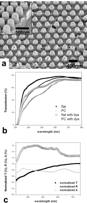
2.4 (a) SEM image of the dense patterns made of an oxide paste without polymeric additives. (b) Transmission spectra of flat and patterned niobium oxide films with and without dye loading. (c) Normalized transmission, reflection, and absorption spectra from a patterned film
relative to a flat film as a function of wavelength………...…40
2.5 (a) Transmission spectra of flat and patterned films with mesoporous top layers. (b) Normalized transmission of the PC sample relative
to the flat film………...….41
2.6 IPCE of flat and PC samples. (a) IPCE of flat and patterned (PC) niobium oxide anode; (b) the normalized IPCE of flat and PC samples at 530nm and (c) the normalized IPCE of PC relative to IPCE of flat
film, revealing an enhancement of IPCE in the blue range……….44
3.1 Procedures for forming mesoporous patterned titania electrodes for the DSSC…….52
3.2 SEM images of the patterned surfaces: rectangular line patterns with different spacing ((a) 250nm, (b) 500nm, (c) 750nm) and cylindrical post in hexagonal array (d) and (e). The crosssection view in (e) reveals that the base layer and PRINT layer formed a monolayer without an interface. Scales were 10µm in large images and 1µm in small images.
(Scales are 1µm in the insets and 10µm in the larger figures.)………....57
3.3 Comparison of two types of integration spheres for evaluating absorption of sensitized TiO2 samples. (a) The samples is placed at the entrance window of the IS and some portion of light can be neglected, leading to overestimation of absorption. (b) As the sample lies inside the IS, all of the light except that which is absorbed is
measured by the detector……….58
3.4 Absorption spectra of samples measured in the integration sphere. The spectra shown in (a) were smoothed to remove noises for easier comparison. Spectra shown in (b) were obtained by normalizing
spectra in (a) at 530nm……….………59
3.5 Absorption spectra of sensitized TiO2 with or without surface PC structure embedded in the electrolyte: T and R were measured by the IS shown in Figure 3.3 (a) and absorption was calculated by the
relationship A=1-T-R………...61
(1~6) TiO2 films before dye loading.………..….62
3.7 (a) Incident photon-to-current conversion efficiency (IPCE) of selected samples and (b) after normalization to the IPCE of flat sample. The IPCE curves of patterned samples all exhibit enhancement at the whole
wavelength range……….65
3.8 (a) Photocurrent density vs. photovoltage (J-V), (b) Open circuit
voltage (Voc), (c) short circuit current (Jsc), (d) global efficiency, (e) fill factor (FF), (f) thickness, (g) Jsc per unit thickness, and
(h) maximum power per unit thickness of flat and Patterned samples…...………….68
3.9 Thickness variation in a sample by position: (a) 12.13µm near the
left edge and (b) 14.11µm at the center region……….……...71
3.10 Simulated absorption spectra of flat (G0) and line-patterned groups (G1~G3)……..73
3.11 Normalized reflection of line-patterned groups to the flat (G0). The simulation was performed at the domain near the surface
as shown in the figure………...73
3.12 Schematic representation of reflection measurement (up) and normalized
reflection of G3 (250/750) to the G0 (flat)………...…...74
3.13 Simulated field strength of (a) 360nm and (b) 700nm light waves in the flat and 250/750 line-patterned sensitized layers of 12µm thick. (c) and (d) are showing the region close to the sensitized layer/electro-
lyte boundary………...77
3.14 Forbidden emissions by the photonic crystal structure………78
3.15 Calculation of reflection extended to 1.5µm wavelength IR by 2µm thick flat and patterned slabs by tilting angles. As the sensitized media is highly absorbing, 0 to 30 was considered to simulate the
radial radiation………...79
4.1 Comparison of the flat and patterned architecture of ITO layer
depicting reduced electron diffusion length to the TCO in the DSSC………...…….87
4.2 Procedures for the fabrication of the anode of the DSSC with
patterned ITO geometry……….………..88
4.3 SEM images of the patterned ITO and cross-sections of TiO2/patterned
TCO architecture for anode of the DSSC………...……….……92
coated glass substrate: (a) transmission by the flat ITO layer is larger than those of patterned ITOs in the whole wavelength range measured and (b) normalized transmission spectra of patterned samples to the flat ITO layer reveal fluctuation between patterned samples. The discrepancy between
flat and patterned geometry is distinct especially in the blue region.………..….…...94
4.5 Resistivity of ITO films at various calcination conditions: 2K/min to final temperature without holding under mild air stream (◊), 2K/min to final temperature with 1hour holding time in the closed quartz tube (○), and
additional H2/N2 treatment at 300C (□)……….………….96
4.6 Summary of photoelectrochemical performance data of DSSCs
with/without ITO structures of various thermal history. Selected incident photon-to-current conversion efficiency (IPCE) and photocurrent
density (J)-photovoltage (V) curves are also shown……….…………...98
4.7 Electrochemical impedance spectroscopy (EIS) results: Nyquist plot (left)
and Bode plot (right), respectively………..………..………….104
5.1 Mesoporous aligned structure fabricated by PLD method………116
5.2 (a) TiO2 nanowires grown all over the substrate and (b) side view re-
vealing that the nanowires were grown on the Au-doped TiO2/Si substrate……...117
5.3 TEM image of 2-dimensional hexagonal mesoporous SnO2 along
[001] zone axis...118
5.4 Double gyroid structure as an example of bicontinuous mesoporous structure……119
5.5 Schematic representation of the photoelctrochemical water splitting by using a hematite electrode in (a), and tandem cell architecture to provide appropriate bias to the hematite electrode in (b). The tandem cell structure takes advantage of the mismatch in band gap energy of hematite and dye
LIST OF ABBREVIATIONS AND SYMBOLS
A(λ) Absorption
AAO Anodic aluminum oxide
AFM Atomic force microscopy
ALD Atomic layer deposition
AM Air mass
AMOL Absorbance modulation optical lithography
CCE Charge collection efficiency
CIE Charge injection efficiency
CVD Chemical vapor deposition
DSPEC Dye-sensitized photo-electrochemical cells
DSSC Dye-sensitized solar cell
EIS Electrochemical impedance spectroscopy
EQE External quantum efficiency
FF Fill factor
FTO Fluorine-doped tin oxide
I Current
IPCE Incident-photon-to-current conversion efficiency
IS Integration sphere
ITO Tin-doped indium oxide
J Current density
Jm Photocurrent at the maximum power point
LHE Light harvesting efficiency
Mw Molecular weight
MIMIC Micromolding in capillaries
NP Nanoparticle
Pinj Incident power to the DSSC
PBG Photonic band gap
PC Photonic crystal
PDMS Polydimethylsiloxane
PFPE Perfluoropolyether
PLD Pulsed laser deposition
PS Polystyrene
PU Polyurethane
PV Photovoltaic
R(λ) Reflection
REM Replica molding
RIE Reactive ion etching
SAED Selected area electron diffraction
SAMIM Solvent-assisted micromolding
SEM Scanning electron microscopy
T(λ) Transmission
TCO Transparent conductive oxide
TEM Transmission electron microscopy
Vm Photovoltage at the maximum power point
Voc Open circuit voltage
XRD X-ray diffraction
Global efficiency
µCP Microcontact printing
µTM Microtransfer molding
CHAPTER 1
LITERATURE REVIEW OF AND INTRODUCTION TO SOFT-LITHOGRAPHY AND DYE-SENSITIZED SOLAR CELLS
1.1 Introduction to soft-lithography
In this section, I provide a brief review of nanopatterning methods focusing on the
conventional photolithographic technologies and the newly developed soft-lithographic
methods.
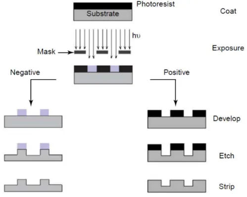
1.1.1 Photolithography
Photolithography is a technique to utilize UV lights, photomasks, and photoresists to
fabricate patterns.1 Figure 1.110 shows a typical nanopatterning processes using conventional photolithograpy. A thin photoresist layer was spin-coated onto the substrate (first step of the
Figure 1.1) and exposed to UV radiation to develop a nanopattern in the photoresist on the
substrate. In this step, usually a projection-printing system is utilized for projecting the
image/pattern on the photomask in reduced size onto the photoresist thin film.13,14 By proper etching and removal of the residual photoresist, nanopatterns are subsequently formed on the
substrate. Since photolithography utilizes projections of images at the photomasks onto the
photoresist to transfer the nanopatterns, the resolution of the nanopatterns are determined by
the precision of the optical system. It is widely known that shorter wavelengths are critical to
getting smaller resolution in optical microscopy.1 So, UV wavelengths used for photolithography have moved to shorter wavelengths, e.g. 436nm (g line of Hg lamp,
resolution of the nanostructure: 500nm), 365nm (i line of Hg lamp, 350nm resolution),
248nm and 193nm (KrF and ArF excimer laser respectively).1,14 However, higher resolution could be achieved even with the same wavelength of UV in combination with delicate optical
technologies like phase shifting masks,15 immersion optics,16,17 or the absorbance modulation optical lithography (AMOL)18 to overcome the wavelength limitation. For further reduction of feature sizes below 100nm, advanced lithographic techniques such as electron-beam
lithography22 are required. On the other hand, there are several problems with the fabrication of nanopatterns that depend on the photolithographic methodology: adaption of these new
technologies inherently results in a spike in the manufacturing costs;14 moreover, photolithography can basically be applied only to flat surfaces due to its optical nature.1,14 Moreover, with the spreading of nanopatterning technologies beyond microelectronics, there
arose strong needs for nanopatterning techniques which can form nanostructures not only
simply with photosensitive materials, but with various functional materials to pattern
functionalities on the surface,23 e.g., proteins on the surface,24 or organic photovoltaic materials.25 So, new methods for nanopatterning which are easily accessible to scientist in various fields and are low cost became necessary. The new technology should also be able to
pattern various functional materials below the micrometer scale, even onto non-flat surfaces.
1.1.2 Soft-lithography
As nanotechnologies become mature and widespread in various fields of sciences and
engineering over the last couple of decades,26-29 the manufacturing cost of the nanopatterning techniques has become a more important factor to researchers in various fields. To the
biological scientists and materials scientists who require a number of experiments,
nanopatterning techniques have still been difficult to access and expensive14 to manage for the bulk of experiments, in part because nanopatterns fabricated by state-of-the-art
techniques are expensive and are usually just for one-time use. So, there has been a strong
demand for new techniques which enable the construction of nanopatterns at a resolution on
the ~100nm level with reduced expense.10,14
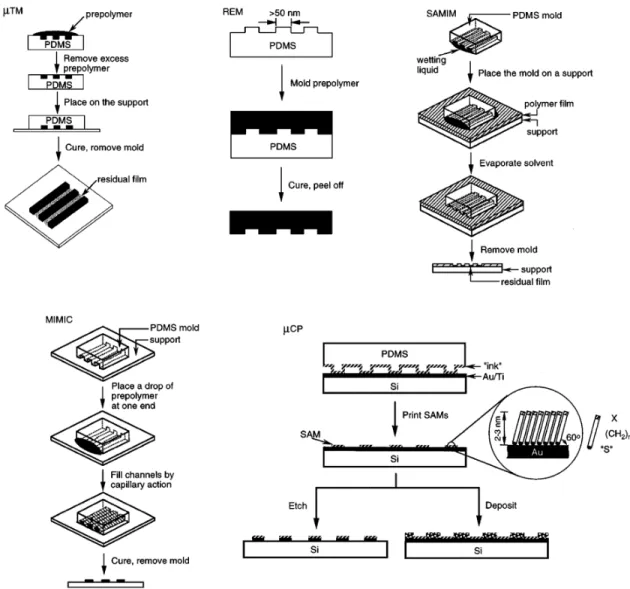
Whitesides and coworkers have opened a new field called ‘soft-lithography’ which
enabled low cost fabrication of nanopatterns on the lab-scale in the 1990s:14,23,29 instead of building new nanopatterns with photolithography every time, they reproduced nanopatterns
by adapting soft elastomers which are the ‘replicas’ of the expensive master nanopatterns
made by conventional photolithography. Polydimethylsiloxane (PDMS) has been the main
elastomer since the invention of the soft-lithography,14 and other polymeric materials such as polyacrylates,30 polyurethane (PU),31 fluoropolymers,32,33 polyolefins,34 polycarbonates.35 Recently, a new fluoropolymer, perfluoropolyether (PFPE) was developed and intensively
used for nanopatterning by DeSimone and coworkers.36-38 PFPE has advantages such as high permeability of vapors, higher strength, and low surface energy compared to the prevailing
PDMS.37
capillaries (MIMIC),42 and microcontact printing (µCP),43 depending on the physical and chemical characteristics of the methods. Figure 1.229 is a schematic representation of the specific soft-lithography techniques listed above.
1.2 Dye-sensitized solar cells (DSSCs)
With the predicted exhaustion of current fossil energy resources, extensive and
intensive research is ongoing for the realization of solar energy, one of the attractive
sustainable energy technologies.44 According to Grätzel,45 as the solar energy supplied in a year is estimated to be 3μ1024J, more than 104 times of the annual energy consumption by human civilization. Energy produced by photovoltaic (PV) cells with just 10% conversion
efficiency covering 0.1% of the earth’s surface could supply sufficient energy to mankind. In
the history of PV technology, initial PV cells have been dominated by solid-state junction
devices based on crystalline or amorphous silicon which could be readily adapted to the
built-in technologies of the silicon semiconductor industries,45 as is evident in Figure 1.3.46 The dye-sensitized solar cell (DSSC) has been one of the emerging photovoltaic cells
with very low production costs since the first report of 7.1% efficiency by O’Regan and
Grätzel in 1991.47 By the combination of better dye molecules absorbing a wider spectrum of sunlight,48-52 and/or new electrolytes with enhanced transport,53-55 their efficiency exceeded 12% in 2011,55 and current world record is 15%.56
In this section, I present brief explanations of the basic operating principles of the
DSSC. Also, I introduce the research trends and issues associated with the improvement of
Figure 1.3 Best research cell records of various types of PV cells by timeline. (This figure is reprinted with permission by the National Renewable Energy Laboratory, http://www.nrel.gov/ncpv/images/efficiency_chart.jpg.46 Accessed July 24, 2013.)
1.2.1 Basic principles and terms of DSSCs
As anatase nanoparticle TiO2 has a band gap energy of 3.2eV,57 which corresponds to the photon energy of the UV light, it is not a proper material for photovoltaic cells as it is,
because it cannot absorb and utilize a large portion of sunlight, i.e., the visible and the IR. So,
in DSSCs, TiO2 nanoparticles are sensitized with a mono layer of dye molecules which
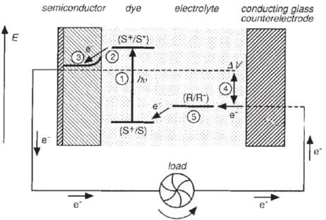
absorb a wide spectrum of sunlight and inject excited electrons to the underlying supporting
TiO2, and the electrolyte transferring electrons to the holes in the dye molecules.45 As DSSCs solely depend on the monolayer of dye molecules to harvest photons and produce electrons,
mesoporous morphology consisting of nanoparticles around 20nm; this provides sufficient
internal surface area—a factor of 1000 greater than the arial area.48 The injected electrons diffuse through the nanoparticle network to be finally collected by an FTO film before
flowing to the counter platinized electrode through an external circuit. The typical electrolyte
contains iodide/triiodide (I-/I3-) ions:45 when a dye molecule (denoted by S in its stable state) absorbs a photon to give an excited electron in its LUMO level (S*), it can inject the electron
to the TiO2, and thereby leave a hole in the HOMO of the dye (S+). Finally, the I- ions in the
electrolyte regenerate the dye (S+S) and transform to I3, which can be oxidized again to the I- ion at the platinized counter electrode. The schematic representation of the operation principle of the DSSC is summarized in Figure 1.4.47
Figure 1.4 Schematic representation of the operation principle of DSSC. (Reprinted with permission from reference 47. Copyright © 1991 Nature Publishing Group)
Generally, DSSCs are composed of a photoanode which is a sensitized TiO2 film on
the transparent conductive oxide (TCO) electrode (typically the fluorine-doped tin oxide
for regeneration of dye molecules. For enhanced stability, solid state DSSCs with the solid
hole-conducting organic layer were reported58 to avoid liquid electrolytes which are less stable and difficult to seal.
Characterization of the solar energy conversion performance of DSSCs is basically
evaluated by the incident-photon-to-current conversion efficiency (IPCE) measurement as a
function of photon wavelength, and the J-V (or I-V) measurement under simulated sunlight,
typically called AM1.5 (100mW/cm2, full sunlight).58 IPCE is the ratio of the number of electrons collected at the external circuit to the incident flux of (monochromatic) photons on
the sensitized TiO2 films, generally expressed as equation 1.47
IPCE λ LHE λ φ (1.1)
Here, LHE λ is the light harvesting efficiency, φ and are charge injection efficiency
(CIE) and charge collection efficiency (CCE), respectively. The details of the LHE, CIE, and
CCE will be discussed in the next section. IPCE is also called the external quantum
efficiency (EQE).59 As IPCE indicates the conversion efficiency as a function of wavelength, it is especially useful when combining a photonic crystal geometries with DSSCs.59-61
The J-V (or I-V) measurement shows the maximum photovoltage (called as the open
circuit voltage), photocurrent (short circuit current), and power output of the DSSCs. By
linearly sweeping potentials (typically from -1V to 1V interval), resultant current is
monitored with and without illumination. The J-V curve in the dark reveals the electrical
maximum power output and/or global efficiency () of the cell, and the fill factor (FF). The
open circuit voltage, Voc, is the maximum voltage in the J-V curve when the DSSC is in an open circuit condition, i.e. the net external current is equal to 0. So, under open circuit
conditions, as the external current is equal to zero, electrons injected to the TiO2 network
from the dye molecules should be balanced by the electron back transfer from the conduction
band of TiO2 to the I3- ions in the surrounding electrolyte.63 The measured open circuit voltage is the difference between the quasi Fermi level of the TiO2 and the redox potential of
the triiodide/iodide ions in the electrolyte,45 as shown in Figure 1.4 (noted as V in the
figure). The short circuit current density, Jsc, is the maximum photocurrent density flowing out to the external short circuit. So, the measured short circuit current is the flow of
photoelectrons injected by the dye molecules into the TiO2 nanoparticle network, and
diffused through it to the FTO layer, and flew out to the external short circuit.63
In real conditions, utilization of both maximum photocurrent and photovoltage is
impractical, due to the series resistance and finite shunt resistance not perfectly suppressing
alternative pathways for electron transfer.64 So, by multiplying the photocurrent density (in mA/cm2) and the photovoltage (V) of every point in the J-V curve, one can get the maximum
power output. Using the maximum power output conditions (Jm and Vm in the Figure 1.5), the fill factor (FF) of the cell can be obtained as the ratio of the value JmμVm (area of the rectangle in orange color in the figure) to JscμVoc (denoted as the rectangle in blue color in the figure). Equation 1.2 is the global efficiency () of the DSSCs using the fill factor.47
Here, Pinc is the incident power to the DSSC in measurement, usually 100mW/cm2 corresponding to the solar energy density of AM1.5.58 Very recently, the Grätzel group reported an efficiency of 15%, the world record of the (solid state) DSSC so far.56
Figure 1.5 Schematic representation of the typical J-V curve under illumination. The ratio
JmVm/JscVoc is the fill factor which is graphically indicated by two rectangles in blue and orange colors.
1.2.2 Issues for the enhancement of the power conversion efficiency
Photoelectrochemical solar energy conversion processes occurring in DSSCs are
thoroughly summarized in numerous references.45,47,62 The widely accepted steps are ‘light harvesting’ of incident photons followed by the ‘charge injection’ from the dye molecules to
the TiO2 nanoparticle network, and charge collection processes. 45, 47, 48, 65,66
The light harvesting efficiency (LHE) is related to the photon absorption process by
oxide semiconductor (typically TiO2) should load a sufficient amount of dyes for maximized
absorption. Currently, the light absorption of sensitized TiO2 film of typical thickness
(10µm~) at the absorption peak of dye molecules (N3 or N719) reaches close to unity.45,66 It also depends on the characteristics of the dye species: there are several brilliant advances in
developing new dye molecules absorbing more photons over a wider sunlight spectrum, e.g.
N3,48 N719,50 Black dye,49 and C101.52 In summary, high LHE is achieved by the combination of the optimized nanostructure accommodating as much dyes as possible and
good dye molecules which can absorb more photons over wide wavelength range. There have
been efforts to enhance LHE through the application of photonic crystal structures which can
reflect unabsorbed photons back to the sensitized TiO2 layer and increase the chance of
additional absorbtion.59,61,67 The DSSCs combined with the photonic crystal structure will be discussed in the separate section later.
The charge injection efficiency (CIE) is the quantum yield for charge injection,47 i.e. the efficiency of the photoelectron injection from the dye molecule into the nanoparticle
network of the metal oxide semiconductors. According to Grätzel,45 the electronically excited dye state is deactivated so quickly (with a rate of 103~1010 s-1), that charge injection should occur about 100 times faster than the deactivation process. Indeed, the well-developed dye
molecules like commercially available N3 and/or N719 also have CIEs close to unity,48,51,66 which means that charge injection occurs in picoseconds, i.e. with a rate of 1012 s-1.45
The charge collection efficiency (CCE) is the efficiency of collecting injected
electrons.47 Injected electrons travel along the complex network of TiO2 nanoparticles which is surrounded by the electrolyte containing iodide/triiodide redox couples and cations. Many
drift, but the diffusional process due to the shielding of Coulomb potential of electrons by the
cations in the electrolyte which in turn, prevents the formation of the electric field in the
mesoporous TiO2 film that enables charge drift.68 Some researchers showed that diffusing electrons spend 10-3 to 100 seconds in the nanoparticle network experiencing trap/detrap processes of ~106 times before harvested by the FTO layer.69 Most of the trap states are provided by the interfacial defects between nanoparticles, and electron back transfer occurs
mainly from the trap states of the nanoparticle network to the I3- ions in the electrolyte.44 Moreover, even after collected by the FTO layer, electron back transfer can occur from the
FTO layer to the electrolyte.63 These electron back transfer pathways give basic ideas on how to improve the CCE: cover the FTO layer with a dense barrier coating,54,66,70,71 and/or form TiO2 structures with less interfacial defects, and/or reduce the diffusion length of electrons
to the TCO.44,66 TiCl4 treatment has been reported as an effective method for forming a dense TiO2 barrier coating on the FTO layer in order to suppress electron back transfer.48,70,72-74 In an effort to reduce the diffusion length from the charge generation point to the FTO as well
as the number of interfacial defects, TiO2 layers comprised of 1-dimensional (1D) geometry
were reported in the form of nanowires73,74 and nanotubes.75,76 Nevertheless, as these 1D geometries inevitably have reduced surface area for the dye monolayer, their overall power
conversion efficiencies were not comparable to that of conventional random nanoparticle
1.2.3 Photonic crystal (PC) structures
A photonic crystal is a periodic optical structure on the wavelength scale (several
hundred nanometers) which can control the propagation of photons.82 Joannopoulos et al.83 used an analogy to explain the nature of photonic crystals: just as periodic electrostatic
potentials of atoms can control the propagation of electrons in the crystals, periodic array of
refractive index contrast on the wavelength-scale can alter the propagation of photons. Figure
1.6 shows the analogy between electronic bandstructure of Si atoms in diamond structure and
photonic bandstructure of dielectric particles (=12) in a diamond structure.83
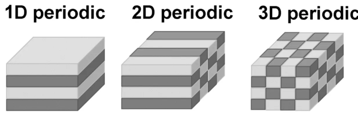
Photonic crystals originate from the work of Yablonovitch84 and John85 in 1987. Historically, Lord Rayleigh observed a photonic band gap from a 1-dimensional stacking of
aternative refractive index materials,82,83 as shown in Figure 1.7 (left).82 This phenomenon is actually very frequently found in nature, e.g. iridescence of butterfly wings.83 However, Yablonovitch and John’s work showed the extension of the photonic band gap concept to
more than 1-dimension, and successfully drew strong attention from researchers. Since then,
researcher have focused on finding new 2- or 3-dimensional (3D) photonic crystal structures
Figure 1.6 Electronic bandstructure of Si atoms in diamond structure (left) and photonic bandstructure of dielectric spheres in diamond structure showing the analogy of control of electron motion in the periodic electrostatic potential and photons in the periodic refractive index contrast. (Reprinted with permission from reference 83. Copyright © 2003 Elsevier Ltd.)
Historically, the realization of a complete photonic band gap with 3D structures of
high refractive index materials like Si has been challenging requiring expensive, multistep
photolithographic techniques that depend on ‘top-down’ approaches.82 The self-assembly of colloidal building blocks provided a much easier way to fabricate 3D photonic crystal
structures.87 One of the most popular 3D photonic crystal structures of this type is the inverse opal structure,88 which is the inverse structure of a FCC array of monodisperse particles. Figure 1.888 shows an inverse opal 3D photonic crystal and the resultant optical characteristics. As shown in the figure, at the wavelength corresponding to the photonic band
gap, an abrupt drop of transmission and an increase in reflection can be seen. So, if the
inverse opal photonic crystal layer is combined with a sensitized mesoporous TiO2 layer in
the DSSC, photons that are not absorbed (or harvested) by the sensitized TiO2 layer cannot
propagate through the photonic crystal layer but are reflected back to the sensitized layer and
can be “reused.”59-61
In DSSCs, polystyrene (PS) is the popular material for the FCC array, because once
the FCC array is formed, it is easy to make the inverse structure by filling the interstitial
spaces between PS spheres with oxide precursors and then removing the PS by
calcination.59,61 Bilayer structures of inverse opal photonic crystal in conjuction with a sensitized TiO2 mesoporous layer59-61 is the typical architecture in the photonic crystal DSSCs. Figure 1.961 shows the complex multistep processing required to build such an architecture. By changing the diameter of the PS spheres, one can easily tune the photonic
photonic crystal structures easily to the DSSCs, and has been the source of interfacial defects
at the sensitized TiO2/inverse opal layer interface. So, the usefulness of light scattering
inverse opal layer has been controversial59-61 and reports dealing with a sufficient number of samples—enough for statistics need to confirm the enhancement of the power conversion
efficiency by photonic crystals—are rare in the literature.61 So, there is a strong demand for new photonic crystal structures with simpler fabrication processes.
Figure 1.9 Complex multistep processes for building inverse opal/mesoporous TiO2 bilayer structure. (Reprinted by permission from reference 61. Copyright 2008 © American Chemical Society)
1.3 Scope of thesis
In section 1.1, I reviewed the history and challenges of conventional photolithography
and their limitations when applied to the research outside of microelectronics, ie. in terms of
cost and versatility of applicable materials. Soft-lithographic techniques which can be used to
fabricate nanostructures and patterns with relative ease and at much lower cost by using
reproduced elastomers were also introduced. As the soft-lithographic techniques are
appropriate to deal with liquids and viscous pastes to fill the replica patterns in the elastomer,
they can be adapted to build special nano/micro structures in the DSSCs by just slightly
modifying the conventional doctor blading process.
In section 1.2, the operation principles of DSSCs and related issues were introduced
in terms of light harvesting, charge injection, and charge collection issues. Basic principles
needed to enhance the CCE were discussed based on those working mechanisms, and then
photonic crystals were also reviewed as candidate structures to enhance the LHE of DSSCs.
complex, multi-step processes, a new photonic crystal structure which can be built by simpler
methods with good structural integrity is worth pursuing.
Consequently, in this thesis, I suggest new architectures for DSSCs that aim to
increase the solar energy conversion efficiency. The modified DSSC structures focus on the
improvement of the LHE and CCE, and most importantly easier fabrication of those
structures. For modification of the conventional DSSC structures, I apply soft-lithographic
techniques based on the PFPE elastomers.
In chapter 2 and 3, I suggest surface patterns for simpler photonic crystal geometries.
As surface patterns can simply be built on the conventional mesoporous TiO2 or other metal
oxide semiconductor layer by adding just one more step using the identical oxide paste, a
seamless photonic crystal structure with the conventional DSSCs can be fabricated without
major structural alterations. In chapter 2, Nb2O5 was used for the supporting mesoporous
nanoparticle network, with a thickness around 3µm, which is about 30% of the conventional
sensitized layer thickness of DSSCs. Fabricated nanostructures were discussed focusing on
their nanostructures and optical behavior in terms of LHE enhancement. IPCE was used as a
measure of solar energy conversion efficiency. In chapter 3, TiO2 nanoparticle networks were
used for light harvesting media. Surface patterns were fabricated to form photonic crystal
geometries by adapting soft-lithography methods. Characterization of the surface patterned
photoanodes focus on the optical behavior of surface patterned structures and their solar
energy conversion by IPCE and J-V measurements.
In chapter 4, structural modification of the TCO was introduced in patterned ITO
substructures for enhancing CCE. The ITO substructures were formed on a micrometer scale
electron diffusion pathways to the TCO electrode. The effects of ITO substructures on the
DSSC performances were analyzed in terms of their morphology, optical change of the
photoanode, and solar energy conversion efficiency in IPCE and J-V measurements.
Electrochemical impedance spectroscopy (EIS) was used to elucidate the characteristics of
the DSSC structure with embedded ITO patterns and suggestions were made based on the
1.4 References
(1) Pease, R. F.; Chou, S. Y. Proc. IEEE 2008, 96, 248–270.
(2) Moore, G. E. Electronics 1965, 38, 114ff.
(3) Vijayakrishnan, V.; Chainani, A.; Sarma, D. D.; Rao, C. N. R. J. Phys. Chem.
1992, 96, 8679–8682.
(4) Likharev, K. K.; Claeson, T. Sci. Am. 1992, 269, 80–85.
(5) Ekimov, A. I.; Onushchenko, A. A. JETP Lett. 1982, 34, 345–349.
(6) Chestnoy, N.; Harris, T. D.; Hull, R.; Brus, L. E. J. Phys. Chem. 1986, 90, 3393– 3399.
(7) Reed, M. A. Sci. Am. 1993, 268, 118–123.
(8) Alivisatos, A. P. Science 1996, 271, 933–937.
(9) Ko, D.-H.; Tumbleston, J. R.; Henderson, K. J.; Euliss, L. E.; DeSimone, J. M.; Lopez, R.; Samulski, E. T. Soft Matter 2011, 7, 6404–6407.
(10) Truskett, V. N.; Watts, M. P. C. TRENDS in Biotech. 2006, 24, 312–317.
(11) Plass, R.; Pelet, S.; Krüger, J.; Grätzel, M.; Bach, U. J. Phys. Chem. B 2002, 106, 7578–7580.
(12) Nozik, A. J. Next Gener. PhotoVoltaics 2004, 196–222.
(13) Okazaki, S. J. Vac. Sci. Technol. B 1991, 9, 2829–2833.
(14) Xia, Y.; Whitesides, G. M. Angew. Chem. Int. Ed. 1998, 37, 550–575.
(15) Levenson, M. D.; Viswanathan, N. S.; Simpson, R. A. IEEE Trans. Electron Devices 1982, ED-29, 1828–1836.
(16) Owa, S.; Nagasaka, H.; Nakano, K.; Ohmura, Y. Proc. SPIE 2006, 6154, 615408.
(17) Sewell, H.; Mulkens, J.; McCafferty, D.; Markoya, L.; Streefkerk, B.; Graeupner, P. Proc. SPIE 2006, 6154, 615406.
(18) Menon, R.; Smith, H. I. J. Opt. Soc. Amer. 2006, A23, 2290–2294.
(20) Warlaumont, J. J. Vac. Sci. Technol.1989, B7, 2934–2938.
(21) Kaesmaier, R.; Löschner, H.; Stengl, G.; Wolfe, J. C.; Ruchhoeft, P. J. Vac. Sci. Technol. 1999, B17, 3091–3097.
(22) Martian, C.R.K.; Snow, E.S. Microelectron. Eng.1996, 32, 173–189.
(23) Wilbur, J. L.; Kumar, A.; Kim, E.; Whitesides, G. M. Adv. Mater.1994, 6, 600–604.
(24) Li, H.-W.; Muir, B. V. O.; Fichet, G.; Huck, W. T. S. Langmuir 2003, 19, 1963– 1965.
(25) Ko, D.-H.; Tumbleston, J. R.; Zhang, L.; Williams, S.; DeSimone, J. M.; Lopez, R.; Samulski, E. T. Nano Lett.2009, 9, 2742–2746.
(26) Wise, K. D.; Najafi, K. Science1991, 254, 1335–1342.
(27) Service, R. E. Science1995, 268, 26–27.
(28) Lee, S. S.; Lin, L. Y.; Wu, M. C. Appl. Phys. Lett.1995, 67, 2135–2137.
(29) Xia, Y.; Whitesides, G. M. Annu. Rev. Mater. Sci. 1998, 28,153–184.
(30) Choi, S. J.; Yoo, P. J.; Baek, S. J.; Kim, T. W.; Lee, H. H. J. Am. Chem. Soc.
2004, 126, 7744–7745.
(31) Kim, Y. S.; Lee, H. H.; Hammond, P. T. Nanotechnology 2003, 14, 1140–1144.
(32) Khang, D.-Y.; Lee, H. H. Langmuir 2004, 20, 2445–2448.
(33) Resnick, P. R.; Buck, W. H. In Fluoropolymers vol. 2: Properties; Hougham, G., Cassidy, P. E., Johns, K., Davidson, T., Eds.; Kluwer Academic Publisher: New York, 1999.
(34) Csucs, G.; Kunzler, T.; Feldman, K.; Robin, F.; Spencer, N. Langmuir 2003, 19, 6104– 6109.
(35) Pisignano, D.; D’Amone, S.; Gigli, G.; Cingolani, R. J. Vac. Sci. Technol. B
2004, 22, 1759–1763.
(36) Rolland, J. P.; Van Dam, R. M.; Schorzman, D. A.; Quake, S. R.; DeSimone, J. M. J. Am. Chem. Soc. 2004, 126, 2322–2323.
(38) Williams, S. S.; Retterer, S.; Lopez, R.; Ruiz, R.; Samulski, E. T.; DeSimone, J. M. Nano Lett. 2010, 10, 1421–1428.
(39) Zhao, X.-M.; Xia, Y.; Whitesides, G. M. Adv. Mater. 1996, 8, 837–840.
(40) Xia, Y.; Kim, E.; Zhao, X.-M.; Rogers, J. A.; Prentiss, M.; Whitesides, G. M. Science 1996, 273, 347–349.
(41) Kim, E.; Xia, Y.; Zhao, X.-M.; Whitesides, G. M. Adv. Mater. 1997, 9, 651–654.
(42) Kim, E.; Xia, Y.; Whitesides, G. M. Nature 1995, 376, 581–584.
(43) Kumar, A.; Whitesides, G. M. Appl. Phys. Lett. 1993, 63, 2002–2004.
(44) Zhang, Q.; Cao, G. Nano Today 2011, 6, 91–109.
(45) Grätzel, M. Inorg. Chem. 2005, 44, 6841–6851.
(46) National Renewable Energy Laboratory (NREL) home page (http://www.nrel.gov/ncpv/images/efficiency_chart.jpg)
(47) O’Regan, B.; Grätzel, M. Nature 1991, 335, 737–740.
(48) Nazeeruddin, M. K.; Kay, I.; Rodicio, A.; Humphry-Baker, R.; Müller, E.; Liska, P.; Vlachopouloss, N.; Grätzel, M. J. Am. Chem. Soc. 1993, 115, 6382–6390.
(49) Nazeeruddin, M. K.; Pechy, P.; Grätzel, M. Chem. Commun.1997, 1705–1706.
(50) Nazeeruddin, M.K.; Zakeeruddin, S.M.; Humphry-Baker, R.; Jirousek, M.; Liska, P.; Vlachopoulos, N.; Shklover, V.; Fischer, C.H.; Grätzel, M. Inorg. Chem. 1999, 38, 6298– 6305.
(51) Wang, P.; Klein, C.; Humphry-Baker, R.; Zakeeruddin, S.; Grätzel, M. J. Am. Chem. Soc. 2005, 127, 808–809.
(52) Gao, F.; Wang, Y.; Shi, D.; Zhang, J.; Wang, M. K.; Jing, X. Y.; Humphry-Baker, R.; Wang, P.; Zakeeruddin, S. M.; Grätzel, M. J. Am. Chem. Soc. 2008, 130, 10720– 10728.
(53) Huang, S. Y.; Schlichthörl, G.; Nozik, A. J.; Grätzel, M.; Frank, A. J. J. Phys. Chem. B 1997, 101, 2576–2582.
(55) Yella, A.; Lee, H.-W.; Tsao, H. N.; Yi, C.; Chandrian, A. K.; Nazeeruddin, M. K.; Diau, E. W.-G.; Yeh, C.-Y.; Zakeeruddin, S. M.; Grätzel, M. Science 2011, 334, 629–634.
(56) Burschka, J.; Pellet, N.; Moon, S.-J.; Humphry-Baker, R.; Gao, P.; Nazeeruddin, M. K.; Grätzel, M. Nature 2013, 499, 316–320.
(57) Tseng, Y.-H.; Kuo, C.-S.; Huang, C.-H.; Li, Y.-Y.; Chou, P.-W.; Cheng, C.-L.; Wong, M.-S. Nanotechnology 2006, 17, 2490–2497.
(58) Bach, U.; Lupo, D.; Comte, P.; Moser, J. E.; Weissörtel, F.; Salbeck, J.; Spreitzer, H.; Grätzel, M. Nature 1998, 395, 583–585.
(59) Guldin, S.; Hüttner, S.; Kolle, M.; Welland, M. E.; Müller-Buschbaum, P.; Friend, R. H.; Steiner, U.; Tétreault, N. Nano Lett. 2010, 10, 2303–2309.
(60) Mihi, A.; Míguez, H. J. Phys. Chem. B 2005, 109, 15968–15976.
(61) Lee, S.-H. A.; Abrams, N. M.; Hoertz, P. G.; Barber, G. D.; Halaoui, L. I.; Mallouk, T. E. J. Phys. Chem. B 2008, 112, 14415–14421.
(62) Yum, J.-H.; Baranoff, E.; Kessler, F.; Moehl, T.; Ahmad, S.; Bessho, T.; Marchioro, A.; Ghadiri, E.; Moser, J.-E.; Yi, C.; Nazeeruddin, M. K.; Grätzel, M. Nature Comm. 2012, 3, 631.
(63) Cameron, P. J.; Peter, L. M. J. Phys. Chem. B 2005, 109, 7392–7398.
(64) Jain, A.; Kapoor, A. Solar Energy Mater. Solar Cells, 2005, 86, 391–396.
(65) Kopidakis, N.; Schiff, E. A.; Park, N.-G.; van de Lagemaat, J.; Frank, A. J. J. Phys. Chem. B 2000, 104, 3930–3936.
(66) Yang, Z.; Xu, T.; Gao, S.; Welp, U.; Kwok, W.-K. J. Phys. Chem. C 2010, 114, 19151–19156.
(67) Colodrero, S.; Mihi, A.; Häggman, L.; Ocaña, M.; Boschloo, G.; Hagfeldt, A.; Míguez, H. Adv. Mater. 2009, 21, 764–770.
(68) van de Lagemaat, J.; Park, N.-G.; Frank, A. J. J. Phys. Chem. B 2000, 104, 2044–2052.
(69) Yang, Z.; Gao, S.; Li, T.; Liu, F.-Q.; Ren, Y.; Xu, T. ACS Appl. Mater. Interfaces 2012, 4, 4419–4427.
(71) Cameron, P. J.; Peter, L. M. J. Phys. Chem. B 2003, 107, 14394–14400.
(72) Barbe, C. J.; Arendse, F.; Comte, P. J. Am. Ceram. Soc. 1997, 80, 3157–3171.
(73) Park, N.-G.; Schlichthörl, G.; van de Lagemaat, J.; Cheong, H. M.; Mascarenhas, A.; Frank, A. J. J. Phys. Chem. B 1999, 103, 3308–3314.
(72) Ito, S.; Liska, P.; Comte, P.; Charvet, R. L.; Péchy, P.; Bach, U.; Schmidt-Mende, L.; Zakeeruddin, S. M.; Kay, A.; Nazeeruddin, M. K.; Grätzel, M. Chem. Commun. 2005, 4351–4353.
(73) Law, M.; Greene, L. E.; Johnson, J. C.; Saykally, R.; Yang, P. D. Nature Mater.
2005, 4, 455–459.
(74) Feng, X. J.; Shankar, K.; Varghese, O. K.; Paulose, M.; Latempa, T. J.; Grimes, C.A. Nano Lett. 2008, 8, 3781–3786.
(75) Zhu, K.; Neale, N.; Miedaner, A.; Frank, A. Nano Lett. 2002, 7, 69–74.
(76) Gong, D.; Grimes, C. A.; Varghese, O. K.; Hu, W. C.; Singh, R. S.; Chen, Z.; Dickey, E. C. J. Mater. Res. 2001, 16, 3331–3334.
(77) Chen, W.; Zhang, H. F.; Hsing, I. M.; Yang, S. H. Electrochem. Commun. 2009, 11, 1057–1060.
(78) Jiang, C. Y.; Sun, X. W.; Lo, G. Q.; Kwong, D. L.; Wang, J. X. Appl. Phys. Lett.
2007, 90, 263501.
(79) Sauvage, F.; Di Fonzo, F.; Li Bassi, A; Casari, C. S.; Russo, V.; Divitini, G.; Ducati, C.; Bottani, C. E.; Compte, P.; Gratzel, M. Nano Lett. 2010, 10, 2562–2567.
(80) Ghosh, R.; Hara, Y.; Alibabaei, L.; Hanson, K.; Rangan, S.; Bartynski, R.; Meyer, T. J.; Lopez, R. ACS Appl. Mater. Interfaces 2012, 4, 4566–4570.
(81) Martinson, A. B. F.; Elam, J. W.; Liu, J.; Pellin, M. J.; Marks, T. J.; Hupp, J. T. Nano Lett. 2008, 8, 2862–2866.
(82) Von Freymann, G.; Kitaev, V.; Lotsch, B. V.; Ozin, G. A. Chem. Soc. Rev. 2013, 42, 2528–2554.
(83) Johnson, S. G.; Joannopoulos, J. D. Acta Mater. 2003, 51, 5823–5835.
(84) Yablonovitch, E. Phys. Rev. Lett. 1987, 58, 2059–2062.
(86) Joannopoulos, J. D.; Johnson, S. G.; Winn, J. N.; Meade, R. D. Photonic Crystals: Molding the Flow of Light, 2nd Ed.; Princeton University Press: Princeton, NJ and Oxford, UK, 2008.
(87) Ozin, G. A.; Hou, K.; Lotsch, B. V.; Cademartiri, L.; Puzzo, D. P.; Scotognella, F.; Ghadimi, A.; Thomson, J. Mater. Today 2009, 12 (5), 12–23.
CHAPTER 2
SURFACE PATTERNING OF MESOPOROUS NIOBIUM OXIDE FILMS FOR SOLAR ENERGY CONVERSION
2.1 Introduction
Since the first report of a high efficiency (~7.1%) dye sensitized solar cell (DSSC) by O’Regan and Grätzel,1 the DSSC has been promoted as a promising photovoltaic technology with lower intrinsic costs compared to conventional Si-based photovoltaic devices. Subsequently, extensive and intensive research has focused on improving DSSC efficiency, mainly by the development of new dye molecules absorbing over a wider spectrum of light,2,3 novel electrolytes,4-6 the design and optimization of cell nanostructures (e.g. tubular7,8 or nanoforests9 of TiO2), and new metal oxides and/or doped materials in addition to titania for dye supports.10-13 Niobium oxide has been a candidate in those efforts to replace TiO2, especially noteworthy for its higher conduction band energy,11,14-17 which can be a benefit in principle by generating a higher open circuit voltage.18 Recently, a high conversion efficiency (4.1%) cell having only a 4µm thick Nb2O5 nanoporous network was reported.19
This chapter is reproduced with permission from Myoung-Ryul Ok, Rudresh Ghosh, M. Kyle Brennaman, Rene Lopez, Thomas J. Meyer, and Edward T. Samulski
Another application of niobium oxide with its higher conduction band energy is a
shell material of the TiO2/Nb2O5 core/shell structured DSSCs, forming an energy barrier to
lower the recombination loss.20,21 Along with the efforts to apply niobium oxide to DSSCs and produce photocurrents, other approaches are underway to use niobium oxide as the wide
band gap semiconductor electrode for solar fuel production, e.g. hydrogen generation with
the dye-sensitized photo-electrochemical cells (DSPECs).22 An additional variable to exploit to obtain better performance with existing materials is to utilize optical structures within the
DSSCs for improving photon absorption and photocurrent generation.23-31 These optical elements have been utilized extensively in TiO2 based DSSCs. Utilizing for instance
additional layer of larger TiO2 particles for effective scattering that confines light in the
dye-sensitized mesoporous TiO2 layer,23 or including a photonic crystal (PC) layer on top of the conventional mesoporous TiO2 film for forming a photonic stop band and reflecting
unabsorbed photons back to the mesoporous TiO2 layer.24-31 In some particularly effective cases, 3-dimensional (3-D) opal-like structures formed with monodisperse polystyrene (PS)
beads were employed to create the photonic crystal layer.24-30 This structure is advantageous because one can easily choose the photonic stop band wavelength by simply selecting the
diameter of the PS beads, especially targeting the red region where intrinsic photon
absorption by the dye molecules is weak.29 However, despite the benefits of the inverse opal based bilayer structures, its construction is a complex multistep processes, limiting the
practical application of PC structures to the DSSCs. Actual enhancements in cell efficiency
the easy and simple methods to fabricate them, and 2-D PCs have been applied to organic
photovoltaic devices34 and solid state DSSCs.35
Herein, I demonstrate a simple surface patterning method based on the
soft-lithographic techniques to form PC structures on the nanocrystalline niobium oxide film
surface. A photo-curable perfluoropolyether (PFPE)36,37 was used to replicate 2-D patterns on a Si master and reproduce them on the surface of mesoporous niobium oxide anodes; the
method exploits the low surface energy and high gas permeability of PFPE.38 Optical characteristics and solar energy conversion performances of the surface patterned niobium
oxide films were analyzed and compared to flat niobium oxide anodes.
2.2 Experimental
2.2.1 Preparation of the niobium oxide paste via sol-gel synthesis
Mesoporous nanocrystalline niobium oxide films were prepared on FTO coated glass
substrates via a sol-gel route. 1.255ml (0.005mol) of niobium ethoxide (Nb(OEt)5, 99.95%,
Aldrich) was dissolved in 10ml of ethanol, and 1ml of this mixture was hydrolyzed with
0.3ml of ammonium hydroxide solution (29.53%, Fisher Scientific). After hydrolysis, 1ml of
glacial acetic acid (99.9%, Fisher Scientific) was added to the hydrolyzed mixture, sonicated,
and stirred overnight for peptization. To this niobium oxide mixture, 1.7ml of hydroxypropyl
cellulose (Mw: 100,000, Aldrich) solution in deionized water (10wt%) was added and well
mixed by stirring overnight. The as-prepared paste was used for mesoporous niobium oxide
base layer and condensed paste was used for additional surface patterning on top of the base
layer.
For surface patterning on top of the calcined niobium oxide films by soft-lithography,
patterned polymeric mold was prepared by following the method reported by Hampton et
al.39: Photocurable PFPE solution (a solution consisting of 1000g/mol PFPE functionalized dimethacrylate and 2,2-diethoxyacetophenone as the photo-initiator) was
poured and spread evenly onto a patterned Si-wafer. The surface pattern used was an
arbitrarily chosen 2-dimensional hexagonal array of cylindrical posts (200nm(D)200nm(H))
with 400nm periodicity which was anticipated to exhibit observable effects in the visible
wavelength range. After purging with N2 gas for 3min, PFPE was polymerized on a Si
patterns by radiating UV light for 3min. The photo-cured PFPE film was carefully removed
from the Si master and rinsed with ethanol to remove uncrosslinked residues on the PFPE
film. Si wafer grade flat PFPE films were also made by using a non-patterned, flat Si wafer
for preparing non-patterned niobium oxide anodes as a control.
2.2.3 Fabrication of mesoporous patterned niobium oxide films
FTO coated glass substrates (15/sq, 2.3mm thick, Hartford glass) were sonicated in
acetone (99.5%, Fisher Scientific), isopropanol (99.9%, Fisher Scientific), and deionized
water for 20min respectively and then heat-treated at 500C in the air for 10min to
completely remove organic residues before coating the niobium oxide paste. Niobium oxide
paste was dropped onto FTO coated glass substrate districted by the tape spacers (3M), dried
on a hot plate (80C), and then calcined in a tube furnace to 600C (2K/min) with mild air
stream.
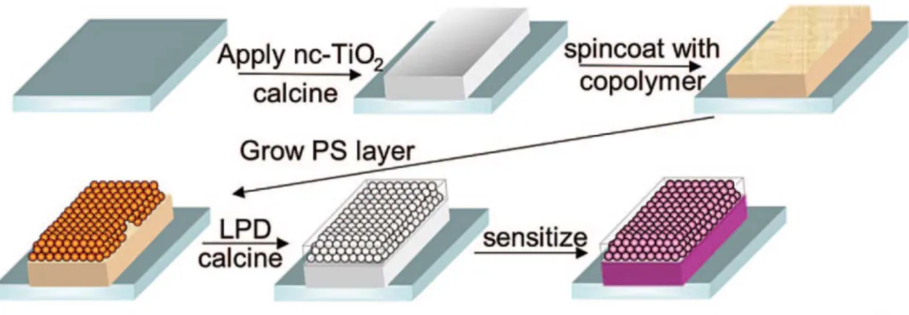
Figure 2.1 summarizes the steps for fabricating surface patterned niobium oxide
films: On top of these flat and patterned PFPE films, a very small amount of condensed
were put onto the calcined niobium oxide layer (Figure 2.1 (a), (b)). Mild pressure was
exerted to the calcined layer/additional paste layer/PFPE-mold assembly to ensure good
mechanical contact among them during the drying step (in an 80C oven). After sufficient
drying, additional niobium oxide paste layer (dried, patterned or flat) and the calcined
niobium oxide film got fused into a single solid entity (Figure 2.1 (c)). Then, the niobium
oxide films with additional dried layer were calcined again in the tube furnace to 600C
(2K/min) with sufficient air stream.
2.2.4 Characterization of the nanostructure of the patterned niobium oxide
Crystallographic characterization was performed with X-ray diffraction (Rigaku
MultiFlex X-ray diffractometer, Cu K radiation, 40kV-40mA, scan speed 4/min) and a
tunneling electron microscope (TEM, 100-CX, JEOL). Morphological information of the
calcined niobium oxide films and surface patterns was obtained with a scanning electron
microscope (SEM, S-4700, Hitachi). UV-visible absorption spectra were collected with an
integration sphere (Cary 5000 fitted with DRA 2500). A surface profilometer (KLA Tencor
P-6, scan speed: 50µm/s, scan length: 5mm) was used to measure the thickness of prepared
films.
2.2.5 Evaluation of the solar energy conversion performances
To evaluate the solar energy conversion performance of flat and patterned niobium
oxide films, prepared films were sensitized with N719 dye and assembled to DSSCs: N719
dye was dissolved to a 1:1 mixture of acetonitrile and t-butanol (0.2 mM), and the solution
was then centrifuged to remove aggregates. Before sensitization, prepared niobium oxide
films were heat treated (500C for 30min) and cooled down to 80C, and carefully
and rinsed with acetonenitrile to wash off unabsorbed portion of dye. The sensitized niobium
oxide films were shaped to ~5mm5mm with a razor blade. Sealed DSSCs were prepared
basically following methods in the literature,40 using a 100 µm Surlyn spacer and drilling one hole for electrolyte injection. The redox electrolyte used was a solution of 0.5 M LiI and 0.05
M I2 in dry acetonitrile. A 75 W Xe Oriel 6251/Oriel Cornerstone 260 monochromator
coupled with a Keithley 6517A current meter was used to measure the incident
2.3 Results and Discussion
2.3.1 Morphological analysis of the patterned niobium oxide films
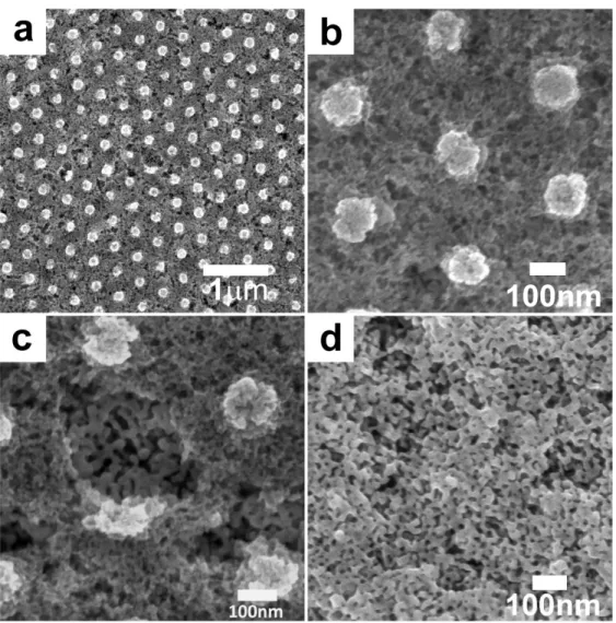
The surface images of the calcined niobium oxide samples are shown in Figure 2.2.
Patterns were well developed maintaining their original periodicity, 400 nm, as shown in
Figure 2.2 (a). One can see that the diameter of the individual features is much smaller than
200 nm, the original diameter of the cylindrical posts on the Si master. As the patterns were
made of a paste containing oxide nanoparticles and a polymeric additive, a large amount of
shrinkage occurs during the calcinations by the removal of the residual solvent and polymeric
phase and interconnection between oxide nanoparticles. However, even with the change in
detailed shape of individual features relative to the original mold, the resulting surface
structures exhibited the periodic 2-D spatial dimensions which constitute a PC geometry. The
surface of the niobium oxide film revealed a mesoporous fine structure of around 10 nm
(based on the smallest dimension) particles, as shown in Figure 2.2 (b). Note that the top
surface shows only the nanostructures of an additional layer formed by patterning; that layer
experienced the calcination process just once whereas the bulk of the niobium oxide base
layer was calcined twice. In Figure 2.2 (c), one can clearly see the bilayer structure through a
defective top layer. The dimensions of the base layer were much coarser than the top layer.
To resolve the morphological discrepancy between the fine top layer and the coarse base
layer, a monolayer with equivalent thermal history to the base layer (double calcinations with
heating rate of 2K/min to 600C) was prepared and observed with an SEM. As shown in
Figure 2.2 (d), a layer with double calcination steps exhibited a bicontinuous mesoporous
structure with coarser particle size about 20~40 nm, which matches well to the image of the
discriminate individual nanoparticles from each other in the SEM images. This implies that
the morphology of the base layer would have been like the fine structure of the top layer
surface shown in Figure 2.2 (b) after the first calcination, and then became coarse and
bicontinuous by the second calcination step. In terms of solar energy conversion, this coarser
but bicontinuous nanostructure could be beneficial in electron transport, while detrimental to
dye loading, in general.