MICROCONTROLLER BASED AUTOMATIC
POWER FACTOR CORRECTION IN MINES
A THESIS SUBMITTED IN PARTIAL FULFILLMENT OF THE
REQUIREMENTS FOR THE DEGREE OF
MASTER OF TECHNOLOGY
IN
MINING ENGINEERING
BY
SMRUTI SUMAN ROUTRAY
ROLL NO- 213MN1497
Department of Mining Engineering
National Institute of Technology
Rourkela -769008
2015
MICROCONTROLLER BASED AUTOMATIC
POWER FACTOR CORRECTION IN MINES
A THESIS SUBMITTED IN PARTIAL FULFILLMENT OF THE
REQUIREMENTS FOR THE DEGREE OF
MASTER OF TECHNOLOGY
IN
MINING ENGINEERING
BY
SMRUTI SUMAN ROUTRAY
ROLL NO- 213MN1497
UNDER THE GUIDANCE OF
Prof. D.P. TRIPATHY
Department of Mining Engineering
National Institute of Technology
Rourkela -769008
2015
National Institute of Technology, Rourkela
CERTIFICATE
This is to certify that the thesis entitled,
“MICROCONTROLLER BASED AUTOMATIC
POWER FACTOR CORRECTION IN MINES”
is being
submitted by
SMRUTI SUMAN
ROUTRAY, Roll No-213MN1497
, in partial fulfillment of the requirements for the award of
degree of
Master of Technology in Mining Engineering
at National Institute of Technology,
Rourkela and is an authentic study analysis work carried out by him under my supervision. To
the best of my knowledge, the matter exemplified in the thesis has not been submitted to any
other university/institute for the award of any degree/diploma.
Dr. Debi Prasad Tripathy
Date: 29
thMay, 2015
Professor
Place: Rourkela
Department of Mining Engineering
National Institute of Technology
Rourkela, Odisha-769008, India
ii
ACKNOWLEDGEMENT
I am greatly thankful to my guide Prof. D. P.Tripathy who acts like a pole star for me during my journey in the research by his infusion, support, encouragement and positive criticism. I express my deep regard to him for the successful completion of this work. His ideas and suggestions were helpful for timely accomplishment of the target aimed. His heart being a great ocean of compassion and love not only created friendly environment during my work with him but also enlightened my soul.
I am grateful to Prof. H. K. Naik, Head of the Department of Mining Engineering, National Institute of Technology, Rourkela, for providing me facilities to carry out my thesis work in the Department and provided inputs when needed.
I would like to thank Mr. S. Sridhar (GM (E&M), MCL) for guiding me regarding the industrial practices and helping me to get some information on the consumption pattern in MCL Mines which proved to be an important part of my project.
I want to extend my gratitude to all the teachers of our department for their affection and support. I am also very thankful to all my classmates and friends who always encouraged me and provided me with suggestions at various steps in completion of this work.
I render my admiration to all my family members and my well-wishers for giving me mental support and inspiration for carrying out my research work. At last my gratitude to the Almighty for having gave the blessings on me to finish this work.
SMRUTI SUMAN ROUTRAY
Roll No: 213MN1497
iii
ABSTRACT
With the mining industry moving from traditional manual methods to the advanced mechanised mining, the focus is also shifting to the energy efficiency of the equipment and system being employed. Most of the equipment used in mining like shovel, drill, elevator, continues miner, conveyor, pumps etc. runs on electricity. Electric energy being the only form of energy which can be easily converted to any other form plays a vital role for the growth of any industry. The Power Factor gives an idea about the efficiency of the system to do useful work out of the supplied electric power. A low value of power factor leads to increase is electric losses and also draws penalty by the utility. Significant savings in utility power costs can be realized by keeping up an average monthly power factor close to unity. To improve the power factor to desired level, reactive power compensators are used in the substations. The most common used device is capacitor bank which are switched on and off manually based on the requirement. If automatic switching can be employed for the correction devices, not only it will improve the response time but also removes any scope for error.
The work carried out is concerned with developing power factor correction equipment based on embedded system which can automatically monitor the power factor in the mining electrical system and take care of the switching process to maintain a desired level of power factor which fulfils the standard norms. The Automatic Power Factor Correction (APFC) device developed is based on embedded system having 89S52 microcontroller at its core. The voltage and current signal from the system is sampled and taken as input to measure the power factor and if it falls short of the specified value by utility, then the device automatically switch on the capacitor banks to compensate for the reactive power. The number of capacitors switched on or off is decided by the microcontroller based on the system power factor and the targeted power factor.
The measurement and monitoring of three different possible load types suggested that only the inductive loads required power factor correction. After employing the correction equipment the targeted power factor of 0.95 is achieved and the increase in power factor varied from 9% to 19% based on the combination of load. There is also a decrease of 1.7% in the total energy consumption due to reduction in load current. The economic analysis for power factor improvement considering the data from a local coal mine suggested the payback period to be around 9 months if the correction equipment is implemented.
iv
ACRONYMS
A Ampere
ATP Alternative Transient Program APFC Automatic Power factor Correction CT Current Transformer
KVA Kilo Volt Ampere
KVAR Kilo Volt Ampere Reactive KW Kilo Watt
kWh kilo Watt Hour
LCD Liquid Crystal Display MCL Mahanadi Coalfields Limited
MSHA Mine Safety and Health Administration PCB Printed Circuit Board
PF Power Factor
PFC Power Factor Correction PT Potential Transformer R Resistive
R-L Resistive-Inductive RMS Root Mean Square
THD Total Harmonic Distortion V Volt
WESCO Western Electricity Supply Company of Odisha ZCS Zero Current Sensor
v
CONTENTS
Sl. No.
Title
Page No.
Certificate
i
Acknowledgement
ii
Abstract
iii
Acronyms
iv
List of Figures
viii
List of Tables
ix
Chapter-1
INTRODUCTION
1-3
1.1
Introduction
2
1.2
Motivation for the Present Research Work
2
1.3
Objectives of the Project
2
1.4
Layout of the Thesis
3
Chapter-2
LITERATURE REVIEW
4-10
2.1
Introduction
5
2.2
Power Factor
5
2.2.1
Reasons of Low Power Factor
6
2.3
Power Factor Correction
6
2.3.1
Static Power Factor Correction
7
2.4
Strategies for Power Factor Correction
7
2.5
Power Factor Compensating Devices
7
2.5.1
Capacitive Compensators
7
2.5.2
Synchronous Condensers
8
2.6
Location of the Correcting Device
8
2.7
Benefits of Power Factor Correction
8
2.8
Overview of Previous Research Work
9
Chapter-3
DESIGN METHODOLOGY
11-26
3.1
Introduction
12
vi
3.3
Algorithm
13
3.4
Flowchart
13
3.5
Measurement
14
3.5.1
Meco Power Guard PG08
14
3.6
Design of Different Loads
14
3.6.1
Design of Pure R Load
15
3.6.2
Design of Series R-L Load
15
3.6.3
Design of Parallel R-L Load
16
Chapter-4
DESIGN & IMPLEMENTATION
17-27
4.1
Introduction
18
4.2
Potential Transformer
18
4.3
Current Transformer
19
4.4
Zero Crossing Detector
19
4.5
Power Supply for Circuit
20
4.5.1
Rectifier
20
4.5.2
Filter
21
4.5.3
Voltage Regulator
21
4.6
Display Unit
22
4.6.1
LCD Connection
22
4.7
Microcontroller
23
4.8
Relay Unit
23
4.8.1
Relay
24
4.8.2
Relay Driver
24
4.9
Capacitor Bank
25
4.10
Circuit Diagram
26
4.11
Hardware Implementation
27
Chapter-5
RESULTS & DISCUSSIONS
28-33
5.1
Introduction
29
5.2
Measurement
29
5.2.1
Analysis of Load Without Correction
29
5.2.2.
Analysis of Load With Correction
30
vii
5.3.1
Monitoring of Load Without Correction
31
5.3.2
Monitoring of Load With Correction
31
5.4
Monitoring of a Real Time Fluctuating Load
32
Chapter-6
ECONOMIC ANALYSIS FOR POWER FACTOR IMPROVEMENT
34-36
6.1
Introduction
35
6.2
Overview of the Lakhanpur Area of MCL
35
6.3
Calculations with a Low Power Factor
36
6.4
Calculations with Improved Power Factor
36
6.5
Calculations for Cost of Correction Equipment
36
Chapter-7
CONCLUSIONS
37-38
7.1
Conclusions
38
7.2
Suggestions for Future Work
38
viii
LIST OF FIGURES
Sl. No. Figure No.
Figure Description
Page No.
1
2.1
Schematic Diagram for Power Factor
5
2
2.2
Different Possible Locations for Capacitor
8
3
3.1
Block Diagram of the Correction Equipment
12
4
3.2
Meco Power Guard PG08
14
5
3.3
Connection Diagram & Circuit Diagram for Pure R Load
15
6
3.4
Connection Diagram & Circuit Diagram for Series R-L
Load
15
7
3.5
Connection Diagram & Circuit Diagram for Parallel R-L
Load
16
8
4.1
A 230/12 Volt Transformer
18
9
4.2
Schematic working of a Current Transformer
19
10
4.3
LM339 IC and its Pin Diagram
20
11
4.4
A Full Bridge Rectifier with Input and Output
21
12
4.5
LM7805 and its Connection Diagram
21
13
4.6
A 16x2 LCD Display
22
14
4.7
Pin Description and Connection Diagram of 16x2 LCD in
4-bit Mode
22
15
4.8
89S52 Microcontroller and its Pin Diagram
23
16
4.9
12 Volt Relay and its Internal Connection
24
17
4.10
ULN2003 Relay Driver and its Pin Connection Diagram
24
18
4.11
Shunt Capacitors
25
19
4.12
Complete Circuit Diagram for the Correction Equipment
26
20
4.13
The Realized PF Correction Equipment
27
21
4.14
The Three Different Types of Load Designed
27
22
5.1
Measuring the PF of a Parallel R-L Load
29
23
5.2
Three Sample Load Patterns for Monitoring
32
24
5.3
Power Factor Variation for Load Pattern A
33
25
5.4
Power Factor Variation for Load Pattern B
33
26
5.5
Power Factor Variation for Load Pattern C
33
ix
LIST OF TABLES
Sl. No. Table No.
Table Description
Page No.
1
5.1
Load Analysis without Correction
30
2
5.2
Load Analysis accompanied by Correction Equipment
30
3
5.3
Monitoring of Load without Correction
31
4
5.4
Monitoring of Load accompanied by Correction Equipment
31
5
5.5
Monitoring of Real Time Fluctuating Load
32
6
6.1
Meter Readings and Consumption of Lakhanpur Area in
March, 2015
National Institute of Technology, Rourkela Page 1
Chapter-1
National Institute of Technology, Rourkela Page 2
1.1
INTRODUCTION
The power factor of an electrical system gives the idea about the efficiency of the system to do useful work out of the supplied electric power. A low power factor leads to increase in losses and also draws penalty by the utility. Modern mining industry using mechanized methods suffers from low power factor due to the use of different electric equipment which requires more reactive power. Significant savings in utility power costs can be realized by keeping up an average monthly power factor close to unity. Utilizing shunt capacitor banks for Power Factor Correction (PFC) is an exceptionally established methodology. The recent trend is to automate the switching procedure of capacitors to get greatest advantage in real time basis. Embedded systems based on microcontrollers can be used to monitor and control the switching of correction devicesbecause of its dependability and execution.
1.2
MOTIVATION FOR THE PRESENT RESEARCH WORK
Electricity plays a pivotal role in almost all businesses, above all in the mining engineering. Without it, it would be hard or nearly impossible for miners to do their task. But since mine sites are often located at the end of the grid and operated with the use of heavy mining machineries, they are particularly susceptible to power issues. With the constantly increasing cost of energy, mining sites are struggling to remain competitive in the market and keep their operation as smooth as conceivable. And since they are also considered very large power users, mines are usually being targeted by electrical companies and related establishments. Retaining the power quality is crucial in mines to maximize production and avoid any technical problems while lowering energy cost. If the power factor approaches 1, it reflects that all the energy supplied in the system is being used resourcefully. But then mine sites often use complex equipment, power factor 1 is not usually obtained. In the mining business, any power factor over .95 is accepted and considered to be an efficient use of energy. The typical uncorrected power factor for a coal mine ranges from 0.65 to 0.8 [1].Amendment of power factor close to unity have the points of interest of diminished utility bills, technical issue evacuation, decreased carbon foot prints, meeting lawful commitment and so forth. Henceforth suitable correction equipment must be designed to monitor the system power factor and make the necessary improvement when it goes underneath the specified limit set as per the standards.
1.3
OBJECTIVES OF THE PROJECT
The primary objective of the project was to design correction equipment which can monitor the
power factor of the mine electrical framework and enhance the power factor to a desired value.
The research investigations were carried out with the following objectives:
National Institute of Technology, Rourkela Page 3
To conduct an electrical survey of the existing system in an opencast mine to study the
system configuration and load patterns, variation of power factor during the mine
operation hours and analyze power factor correction facility, if any.
Design a microcontroller based correction equipment to improve the power factor of the
system to desired value of greater than 0.95.
Implement the system and monitor different electrical load models and diverse load
patterns to verify the result.
To carry out economic analysis for power factor improvement.
1.4
LAYOUT OF THE THESIS
Chapter-1 gives a brief overview of the research area, inspiration driving the work, objectives identified and organization of the thesis.
Chapter-2 consists of literature review for comprehensive interpretation of the concepts associated with power factor and its correction accompanied by the prior research work carried out in this area.
Chapter-3 involves the proposed principle to design the correction equipment and the algorithm to work for achieving the required outcome along with the technique to measure and monitor.
Chapter-4 gives detail idea about construction and working of each component associated with the power factor correction equipment and the final hardware implementation.
Chapter-5 shows the results obtained by measuring and monitoring the designed loads under different conditions and load patterns.
Chapter-6 involvesthe economic analysis and viability of the correction equipment considering data obtained from a coal mine (MCL).
National Institute of Technology, Rourkela Page 4
Chapter-2
National Institute of Technology, Rourkela Page 5
2.1
INTRODUCTION
Efficient utilization of energy is now considered as one of the primary motives in any mechanized industry. The power factor of any electrical system suggests how efficient it is to do the useful work. Most mining machines have notoriously poor power factors because of under-utilization of induction motors. This specifically identifies poor system efficiency and utilization. The large load currents drawn result in poor voltage regulation of the system besides contributing to large joule losses in lines. Diminished voltage levels directly translate into heating of motor windings in this way decreasing the life and reliability of the machine. The decline in available torque, corresponding to the less than nominal voltage, will result in poorer machine performance. The maximum kilovolt-ampere demand charge increases as a consequence of poor power factor, and in most cases forms a rather large part of the monthly utility service charge.
2.2
POWER FACTOR
The power factor (PF) of an AC electrical power system is defined as “the ratio of the real power flowing to the load, to the apparent power in the circuit” [2]. Real power is the capacity of the circuit for performing work in a particular time. Apparent power is the product of the current and voltage of the circuit. Due to energy stored in the load and returned to the source, or due to a non-linear load that distorts the wave shape of the current drawn from the source, the apparent power will be greater than the real power. It is schematically shown in Figure 2.1.
Figure 2.1: Schematic Diagram for Power Factor
A load with a power factor of 1.0 result in the most efficient loading of the supply and a load with a power factor of 0.5 will result in much higher losses in the supply system.
National Institute of Technology, Rourkela Page 6
A poor power factor can be the result of either a significant phase difference between the voltage and current at the load terminals, or it can be due to a high harmonic content or distorted/ discontinuous current waveform. Poor load current phase angle is generally the result of an inductive load such as an induction motor, power transformer, lighting ballasts, welder or induction furnace. A poor power factor due to an inductive load can be improved by the addition of power factor correction, but, a poor power factor due to a distorted current waveform requires a change in equipment design or expensive harmonic filters to gain an appreciable improvement. To have an efficient system the power factor should be maintained near to 1. Utilities typically charge additional costs to commercial customers who have a power factor below some limit, which is typically 0.9 to 0.95.
2.2.1
Reasons of Low Power Factor
Mercury vapour lamps or lamps operated with chokes
Power and distribution Transformers. A complete unloaded transformer is very inductive and has a very low power factor.
Induction motors (Load and unload condition)
The inductive load equipment causing low power factor in the mines includes Hoists, Shovel, Drill, Pump, Shearer, Conveyors etc.
2.3
POWER FACTOR CORRECTION
Power factor correction (PFC) is a technique of counteracting the undesirable effects of electric loads that create a power factor (PF) that is less than 1. Power factor correction may be applied either by an electrical power transmission utility to improve the stability and efficiency of the transmission network or, correction may be installed by individual electrical customers to reduce the costs charged to them by their electricity supplier.
Capacitive Power Factor correction is applied to circuits which include induction motors as a means of reducing the inductive component of the current and thereby reduce the losses in the supply. Capacitors connected at each starter and controlled by each starter are known as "Static Power Factor Correction". Resistive constituent of motor current are:
Load current
Loss current Inductive constituent of motor current are:
Leakage reactance
National Institute of Technology, Rourkela Page 7
2.3.1
Static Power Factor Correction
Static power factor correction is commonly applied by using one contactor to control both the motor and the capacitors. It is better practice to use two contactors, one for the motor and one for the capacitors. Where one contactor is employed, it should be up sized for the capacitive load. The use of a second contactor eliminates the problems of resonance between the motor and the capacitors.
2.4
STRATEGIES FOR POWER FACTOR CORRECTION
Following are different methods of power factor improvement which can be implemented according to the type of load such asconstant or variable [4].
a. Individual power factor correction b. Group power factor correction. c. Central power factor corrections.
i. Fixed power factor regulation ii. Automatic power factor regulation iii. Mixed power factor correction
2.5
POWER FACTOR COMPENSATING DEVICES
The power factor compensating devices essentially supplies the required reactive power of the system to improve the power factor and system voltage profile. Shunt capacitors are the most commonly used compensation device in the industry.
2.5.1
Capacitive Compensators
Shunt capacitors are being extensively used in industrial distribution systems. They supply reactive power to counteract the out-of-phase component of current required by an inductive load. The application of shunt capacitor banks results in a decrease in the magnitude of the source-current, improves the power factor and consequently improves voltage regulation throughout the system. However, shunt capacitor banks do not affect current or power factor beyond their point of application. Capacitor banks can be fixed, switched, or a combination of both. The switching process can be manual or automatic. Capacitor banks are rugged and simple to configure and install [7].
It should be noted that Mine Safety and Health Administration (MSHA), U.S. Department of Labor, is concerned with the installation of power-factor correction capacitors in high-voltage power centers. Even though the capacitors have bleeder resistors, MSHA feels that each capacitor bank should have an alternative built-in means for discharging the capacitors [8].
National Institute of Technology, Rourkela Page 8
2.5.2 Synchronous Condensers
The synchronous motor has long been used as a compensator with fixed ratings (known as a synchronous condenser). Compensation is achieved by setting the field excitation to arrive at a particular rating. A disadvantage of this device is that it is electromechanical and requires some maintenance. Since the degree of compensation is predetermined, as with a fixed capacitor bank, synchronous condensers have little appeal over capacitors [7].Accordingly, their application in the mining industry has been limited, except in cases where salvaged ones were available, at an attractive price.
The points to be considered in any installation are: i. Reliability of the equipment to be installed. ii. Probable life.
iii. Capital cost. iv. Maintenance cost. v. Running Costs.
vi. Space required and ease of installation.
2.6
LOCATION OF THE CORRECTING DEVICE
Strategic location of power factor compensators is necessary to achieve all the aforementioned benefits of power factor correction. There are three possible locations in the mine power system: the distribution side of the main substation transformer; at each motor or on each motor powered machine; in load centers [9].
Figure 2.2: Different Possible Locations for Capacitor [9]
The location can be near the load, near the transformer or at the utility side. The location needs to be decided based on the system, voltage regulation (Figure 2.2).
2.7
BENEFITS OF POWER FACTOR CORRECTION
Improving a facility's power factor can have the following benefits [10]: a. Power Factor Surcharges Encourage Higher Efficiency b. Reduced Demand Charges
National Institute of Technology, Rourkela Page 9
c. Increased Load Carrying Capabilities in Existing Circuits d. Improved Voltage
e. Reduction in Power-System Losses
Capacitors are effective in reducing only that portion of the losses that is due to the kilovars current. Losses are proportional to current squared, and since current is reduced in direct proportion to power factor improvement, the losses are inversely proportional to the square of the power factor. The capacitors have losses, but they are relatively small-only one third of 1 per cent of the KVAR rating.
2.8
OVERVIEW OF PREVIOUS RESEARCH WORK
A limited number of studies have been attempted on the effect of poor power factor in mines and the corrective measures to mitigate the problem.
Oommen and Kohler (1988) explored the advantages that can be accomplished by proper implementation of power factor compensation. Different compensators along with the sizing and strategic location was also considered. A brief study on the economic analysis was carried out to show the economic viability of compensation [7].
Jiang et al. (1993) proposed a novel single-phase power factor correction scheme based on parallel power factor correction concept which was described to be more efficient than convention two-cascade stage scheme [14].
Qureshi and Aslam (1995) outlined the different methods for power factor correction and carried out an experimental case study to explore the areas which will be suitable for compensation. After a practical demonstration to have a significant improvement in power factor was completed, they found that it would release the capacity of distribution transformer and the problem of over voltage under condition of low load was avoided [6].
Novak and Kohler (1998) pointed out the importance of power factor improvement for technological innovation and advancement in deep coal mine power systems. Different protection equipment to check the inherent electrical faults in the mining system were argued. The power factor correction near loads for improved voltage regulation was emphasized within the constraints of high voltage distribution in underground coal mines [8].
Shwehdi and Sultan (2000) suggested some mathematical calculations for power factor and reactive power requirement of the system along with the capacitor size estimation methods. Different problems
National Institute of Technology, Rourkela Page 10
associated accompanied by essentials and cautions for capacitor used for correction purpose were discussed in details [9].
Celtekligil (2008) discussed the application of a method for dynamic power factor correction and voltage regulation in light rail transportation system. Main reactors have been switched on through thyristors using automatic power controllers by sensing the power factor and constantly monitoring the current and voltage, calculating the power factor and switching inductance banks as required. The system proposed connects inductive loads in parallel with the capacitive system to improve the power factor [16].
Choudhury (2008) gave a design and implementation of a low cost power factor improvement device for small signal low power loads. The design involved designing of a small signal model load, selecting appropriate capacitors, and designing appropriate switching circuits to select proper combination of capacitors [17].
Shahid and Anwar (2013) offered the design of a power factor improvement circuit using PIC (Programmable Interface Controller) chip with reduced parts count to achieve desired efficiency and low cost. The solution involves ensuring the power factor value from the load and uses an algorithm to determine and trigger switching capacitors in order to compensate for excessive reactive components to increase power factor value [19].
Sharma and Haque (2014) carried out a simulation and analysis study for power factor correction for metal halide high intensity discharge lamps. A modified boost converter using active devices was proposed along with PI controller to stabilize the control loops. The capacitor and inductor with voltage and current ripple with minimum ripple values was designed and to absorb sinusoidal input current to reduce total harmonic distortion (THD) in the input current with output voltage regulation [20].
Allah (2014) suggested an automatic power factor correction based on Alienation technique. An alienation technique was developed for calculations of original power factor on-line, active and compensation reactive powers and determination of the required number of capacitor banks to get the desired power factor. Alienation coefficients were calculated between phase voltage and current signals of power supply. Alternative transient program (ATP) and MATLAB programs were used to implement the proposed technique [21].
National Institute of Technology, Rourkela Page 11
Chapter-3
National Institute of Technology, Rourkela Page 12
3.1 INTRODUCTION
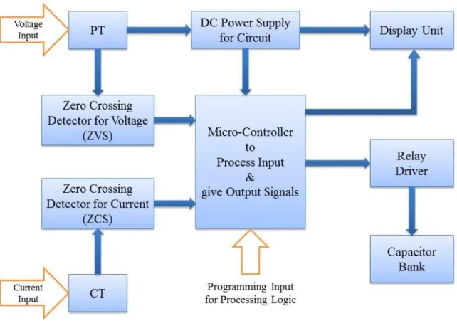
The Automatic Power Factor correction device is developed built on embedded system having 89S52 at its core. The voltage and current signal from the system is sampled and taken as input where the difference between the arrivals of wave forms indicates the phase angle difference. The difference is measured by the internal timer and calibrated as phase angle to calculate the corresponding power factor. The system power factor is compared with the desired level and the difference is measured for switching of required number of capacitors from the bank. The values of power factor and phase lag are shown on a display for convenience.
3.2 BLOCK DIAGRAM
National Institute of Technology, Rourkela Page 13
3.3 ALGORITHM
Step-1: Take input for voltage and current in the circuit. Step-2: Measure the phase lag and calculate the power factor.
Step-3: Differentiate from the targeted power factor and calculate the reactive power requirement. Step-4: Switch ON or OFF appropriate number of capacitors from capacitor bank depending on reactive
power supplied by each step.
Step-5: Again compare the power factor with targeted PF and continue from step-1.
National Institute of Technology, Rourkela Page 14
3.5 MEASUREMENT
The primary quantities to be measured are power factor and energy consumed. Along with these, the voltage level, current flowing and active power will also be helpful for monitoring the load. The instruments used for all required purpose is Meco Power Guard Model PG08 [22].
3.5.1 Meco Power Guard PG08
Using high-integration microcomputer chips and special Energy Metering IC, with high-accuracy current sensor and LCD, this product can monitor electric equipments in every way. It can be used in monitoring domestic appliances such as air conditioner; fridge and microwave oven. This product is suitable for home, rental house, office, laboratory and various places.
Figure 3.2: Meco Power Guard PG08 [22]
3.6 DESIGN OF DIFFERENT LOADS
To verify and monitor the working of the correction device three different types of loads are designed corresponding to actual loads in a typical power system. These will replicate the loading pattern, power consumption, power factor etc.
National Institute of Technology, Rourkela Page 15
3.6.1 Design of Resistive(R) Load
To design a pure resistive load, a light bulb or incandescent lamp of 100W can be used. The circuit connection is shown below.
Figure 3.3: Connection Diagram & Circuit Diagram for Pure R Load The resistor R represents the resistance value of the bulb filament.
Here V=230V, R=550KΩ
According to Ohms Law,
Current, I =
=
=
0.41 mA3.6.2 Design of Series R-L Load
To model an inductive load, a tube light choke can be used. The choke and the bulb connected in series will behave as a series R-L load. The circuit connection is shown below. The voltage available for the bulb will be less than the supply voltage due to the drop in the choke.
National Institute of Technology, Rourkela Page 16
The impedance of the circuit will be, Z= R+jXL
Current, I =
3.6.3 Design of Parallel R-L Load
The choke and the bulb when connected in parallel will behave as a parallel R-L load. The bulb will get the same voltage as the supply. The circuit connection is shown below.
Figure 3.5: Connection Diagram & Circuit Diagram for Parallel R-L Load The impedance of the circuit will be, Z =
National Institute of Technology, Rourkela Page 17
Chapter-4
Design &
National Institute of Technology, Rourkela Page 18
4.1 INTRODUCTION
This chapter describes the detailed design of each block of the proposed power factor correction equipment along with the working of each part. Each block consists of several components connected in the required way to give the desired output. The complete circuit diagram is provided at the end based on which the fabrication was completed. Special care was taken during the fabrication to avoid any short circuit of paths during crossing of paths.
4.2 POTENTIAL TRANSFORMER
Transformers convert AC electricity from one voltage to another with a little loss of power. The potential transformer (PT) essentially uses a step-down transformer to reduce the dangerously high voltage to a safer low voltage (typically 110 Volts) in any substation. The PT used here steps-down the supply voltage of 230 Volts to 12 Volts as required by the circuit to operate. The output of a PT is used for all measurement and monitoring purposes in conjunction with relay operation
Figure 4.1: A 230/12 Volt Transformer [24]
The ratio of the number of turns on each coil, called the turn’s ratio, determines the ratio of the voltages. A step-down transformer has a large number of turns on its primary (input) coil which is connected to the high voltage mains supply, and a small number of turns on its secondary (output) coil to give a low output voltage. Turns ratio = = =
National Institute of Technology, Rourkela Page 19
Where,
Vp = primary (input) voltage.
Vs = secondary (output) voltage
Np = number of turns on primary coil
Ns = number of turns on secondary coil
Ip = primary (input) current
Is = secondary (output) current.
4.3 CURRENT TRANSFORMER
In an electrical circuit, a current transformer (CT) is used for measurement of electric currents. Current transformers, together with voltage transformers (VT) (potential transformers (PT)), are known as instrument transformers. When current in a circuit is too high to directly apply to measuring instruments, a current transformer produces a reduced current accurately proportional to the current in the circuit, which can be conveniently connected to measuring and recording instruments. It also isolates the measuring instruments from what may be very high voltage in the monitored circuit. They are commonly used in metering and protective relays in the electrical power industry.
Figure 4.2: Schematic working of a Current Transformer [26]
4.4 ZERO CROSSING DETECTOR
The zero crossing detector is a sine-wave to square-wave converter. To calculate the phase lag between the voltage and current, two detectors are used to find the arrival instance of each signal. Then the difference in the arrival instance calibrated to angle gives the phase angle lag. By taking the cosine of this phase lag, power factor of the circuit is calculated. The reference voltage in this case is set to zero. The output voltage waveform shows when and in what direction an input signal crosses zero volts. If input
National Institute of Technology, Rourkela Page 20
voltage is a low frequency signal, then output voltage will be less quick to switch from one saturation point to another. And if there is noise in between the two input nodes, the output may fluctuate between positive and negative saturation voltage Vsat. The LM339 IC is used as the comparator circuit to function as zero crossing detector.
Figure 4.3: LM339 IC and its Pin Diagram [27]
4.5 POWER SUPPLY FOR CURCUIT
The embedded system circuit typically uses 12 volt and 5 volt DC as its operating voltage. Therefore, there is a need to convert the 230 Volt AC supply to the required DC supply. In the 1st stage the 230 V AC is step-down to 12 V AC by using a transformer. In this case the output from the potential transformer (PT) can be utilized instead of going for another step-down transformer. The 2nd stage is the rectification process. By using a full bridge rectifier circuit, the 12 V AC is rectified to a 12V pulsating DC voltage. This pulsating DC is passed through a capacitive filter for smoothening in the 3rd stage and gives a normal 12V DC as output. The 4th stage consists of using a 12 V and a 5 V voltage regulator for generating the required stable supply voltage to be used in the control circuit.
4.5.1 Rectifier
A rectifier is an electrical device that converts alternating current (AC), which periodically reverses direction, to direct current (DC), current that flows in only one direction, a process known as rectification. It converts A.C. into pulsating D.C. The rectifier may be a half wave or a full wave rectifier. Most of the cases, a bridge rectifier is used because of its merits like good stability and full wave rectification. In positive half cycle only two diodes (1 set of parallel diodes) will conduct, in negative half cycle remaining two diodes will conduct and they will conduct only in forward bias only.
National Institute of Technology, Rourkela Page 21
Figure 4.4: A Full Bridge Rectifier with Input and Output [29]
4.5.2 Filter
Capacitive filter is used in this project. It removes the ripples from the output of rectifier and smoothens the D.C. Output received from this filter is constant until the mains voltage and load is maintained constant. The simple capacitor filter is the most basic type of power supply filter.
4.5.3 Voltage Regulator
The LM78XX/LM78XXA series of three-terminal positive regulators are available in the TO-220/D-PAK package and with several fixed output voltages, making them useful in a wide range of applications. Each type employs internal current limiting, thermal shutdown and safe operating area protection, making it essentially indestructible. If adequate heat sinking is provided, they can deliver over 1A output Current. Although designed primarily as fixed voltage regulators, these devices can be used with external components to obtain adjustable voltages and currents. In the LM78XX, the output voltage is specified by the last 2 digits XX. The output of LM7805 will be 5 Volts and the same for 7812 will be 12 volts.
National Institute of Technology, Rourkela Page 22
4.6 DISPLAY UNIT
In an embedded system, the microcontroller interacts with the outside world using input and output devices that communicate directly with a human being. One of the most common devices attached to the microcontroller is an LCD display. Some of the most common LCDs connected to the microcontroller are 16x2 and 20x4 displays. This means there will be 16 characters per line by 2 lines and 20 characters per line by 4 lines, respectively available to use. In this project a 16x2 LCD, model JHD 162A which shows the power factor and the phase lag between voltage and current in milliseconds.
Figure 4.6: A 16x2 LCD Display
4.6.1 LCD Connection
The connection to microcontroller requires 3 control lines as well as either 4 or 8 I/O lines for the data bus. The user may select whether the LCD is to operate with a bit data bus or an 8-bit data bus. If a 4-bit data bus is used the LCD will require a total of 7 data lines (3 control lines plus the 4 lines for the data bus). If an 8-bit data bus is used the LCD will require a total of 11 data lines (3 control lines plus the 8 lines for the data bus).
National Institute of Technology, Rourkela Page 23
4.7 MICRCONTROLLER
The heart of any embedded system is a microcontroller which is responsible for all the logical processing. It takes input, processes it according to the program written to it and then gives the processed output. It also has some on chip memory which is utilized to store some temporary variables during processing is going on. The microcontroller used here is AT89S52 which is a 8-bit controller.
The AT89S52 is a low-power, high-performance CMOS 8-bit microcontroller with 8K bytes of in-system programmable flash memory. The device is manufactured using Atmel’s high-density nonvolatile memory technology and is compatible with the industry standard instruction set and pin out. The on-chip flash allows the program memory to be reprogrammed in-system or by a conventional nonvolatile memory programmer. By combining a versatile 8-bit CPU with in-system programmable flash on a monolithic chip, the Atmel AT89S52 is a powerful microcontroller which provides a highly-flexible and cost-effective solution to many embedded control applications. The AT89S52 provides the following standard features: 8K bytes of flash, 256 bytes of RAM, 32 I/O lines, watchdog timer, two data pointers, three 16-bit timer/counters, a six-vector two-level interrupt architecture, a full duplex serial port, on-chip oscillator, and clock circuitry.
Figure 4.8: 89S52 Microcontroller and its Pin Diagram [32]
4.8 RELAY UNIT
This unit consists of a relay driver and some relays. As the output of the microcontroller cannot control the switching of capacitors directly, this unit is responsible for controlling the high power circuit from a low power circuit.
National Institute of Technology, Rourkela Page 24
4.8.1 Relay
A relay is an electrically operated switch. Relays are used where it is necessary to control a circuit by a low-power signal (with complete electrical isolation between control and controlled circuits), or where several circuits must be controlled by one signal. Current flowing through the coil of the relay creates a magnetic field which attracts a lever and changes the switch contacts.
The relay's switch connections are usually labelled COM, NC and NO:
COM = Common, always connect to this; it is the moving part of the switch.
NC = Normally Closed, COM is connected to this when the relay coil is off.
NO = Normally Open, COM is connected to this when the relay coil is on.
Figure 4.9: 12 Volt Relay and its Internal Connection [33]
4.8.2 Relay Driver
As the current supplied by the output pin of microcontroller is not sufficient for the relay coil to operate the relay, a relay driver ULN2003 is used. ULN2003 is a high voltage and high current Darlington transistor array. The ULN2003 is a monolithic high voltage and high current Darlington transistor arrays. It consists of seven NPN Darlington pairs that feature high-voltage outputs with common-cathode Clamp diode for switching inductive loads. The collector-current rating of a single Darlington pair is 500mA. The Darlington pairs may be paralleled for higher current capability. Applications include relay drivers, hammer drivers, lamp drivers, display drivers (LED gas discharge), line drivers, and logic buffers.
National Institute of Technology, Rourkela Page 25
4.9 CAPACITOR BANK
Shunt capacitor banks are used to improve the quality of the electrical supply and the efficient operation of the power system. Studies show that a flat voltage profile on the system can significantly reduce line losses. Shunt capacitor banks are relatively inexpensive and can be easily installed anywhere on the network. The capacitor bank consists of number of shunt capacitors which are switched ON or OFF depending on the reactive power requirement. The switching of capacitors can be done manually or automatically by using relays.
Figure 4.11: Shunt Capacitors [35]
Shunt capacitors, either at the customer location for power factor correction or on the distribution system for voltage control, dramatically alter the system impedance variation with frequency. Capacitors do not create harmonics, but severe harmonic distortion can sometimes be attributed to their presence.
A shunt capacitor at the end of a feeder results in a gradual change in voltage along the feeder. Ideally, the percent voltage rise at the capacitor would be zero at no load and rise to maximum at full load. However, with shunt capacitors, percent voltage rise is essentially independent of load. Thus, automatic switching is often employed in order to deliver the desired regulation at high loads, but prevent excessive voltage at low loads. Moreover, capacitor switching may result in transient overvoltage inside customer facilities.
National Institute of Technology, Rourkela Page 26
4.10 CIRCUIT DIAGRAM
National Institute of Technology, Rourkela Page 27
4.11 HARDWARE IMPLEMENTATION
The PCB was fabricated according to the VRP diagram for the complete circuit and all the components are soldered on it. The connection for potential transformer, current transformer, capacitor bank was done at the respective places. Continuity check using the multimeter was carried out to avoid any accidental short-circuits. The program was written to the microcontroller by using a burner. The complete hardware is shown in the below diagrams (Figs. 4.18 & 4.19).
Figure 4.13: The Realized PF Correction Equipment
National Institute of Technology, Rourkela Page 28
Chapter-5
Results &
Discussions
National Institute of Technology, Rourkela Page 29
5.1 INTRODUCTION
The usefulness of any device designed can only be verified after it is used and expected result is achieved. After the power factor correction circuit is fabricated, it is required to verify the working and desired correction in power factor. For this purpose the measurement of suitable electrical parameters is necessary accompanied by a periodical monitoring of desired outcome.
5.2 MEASUREMENT
All the measurements need to be done for the three different types of load designed; separately with and without the correction equipment. The quantities like supply voltage, frequency, current drawn by the load, power consumed, power factor are essential to be measured for each cases. The energy utilized is also necessary to monitored for a particular duration of time to confirm for the consequent energy savings, if any. The Meco power guard instrument was employed for all the measurement and monitoring.
Figure-5.1: Measuring the PF of a Parallel R-L Load
5.2.1 ANALYSIS OF LOAD WITHOUT CORRECTION
The analysis of the pure restive load (R Load), series resistive-inductive loads (Series R-L Load) and parallel resistive-inductive (Parallel R-L Load) was done without using the correction equipment. The designed loads were connected through the PG08 power guard and the readings for different electrical parameters were recorded.
National Institute of Technology, Rourkela Page 30
Table 5.1: Load Analysis without Correction
Sl. No. Load Type Supply Voltage (Volts) Supply Frequency (Hz) Load Current (mA) Power Drawn (Watts) Power Factor Remarks
1 Pure R 234 49.87 437 101.2 0.99 No Correction Required
2 Series R-L 235 49.92 318 55.3 0.73 Correction Required
3 Parallel R-L 235 49.89 730 129.1 0.76 Correction Required
5.2.2 ANALYSIS OF LOAD WITH CORRECTION
As there is a need for power factor improvement for Series R-L load and Parallel R-L load, they were connected to the supply along with the correction equipment designed to verify the expected correction. The correction equipment is plugged in to the PG08 power guard and the loads are connected to the output point of the equipment. All the three loads designed were tried and the observed values were recorded.
Table 5.2: Load Analysis accompanied by Correction Equipment
Sl. No. Load Type Supply Voltage (Volts) Supply Frequency (Hz) Load Current (mA) Power Drawn (Watts) Power Factor Remarks 1 Pure R 230 50.02 424 96.6 0.99 No Improvement in PF 2 Series R-L 234 50.10 267 59.9 0.96 31.5% Increase in PF 3 Parallel R-L 232 50.06 602 134.2 0.97 29.3% Increase in PF
5.3 MONITORING
Monitoring generally means to be aware of the state of a system and may refer to observe a situation for any changes which may occur over time, using a monitor or measuring device. To measure the energy consumed, it is necessary to monitor the load for a specific period of time. The Meco PG08 power guard can be used to monitor the time as well as measure the energy consumption for each type of load. The loads are connected continuously for the definite time and continuous monitoring was done with extreme care.
National Institute of Technology, Rourkela Page 31
5.3.1 MONITORING OF LOAD WITHOUT CORRECTION
The monitoring of the pure restive load (R Load), series resistive-inductive loads (Series R-L Load) and parallel resistive-inductive (Parallel R-L Load) was done without using the correction equipment. The designed loads were connected through the PG08 power guard and the readings for energy consumption, time and average power factor were recorded.
Table 5.3: Monitoring of Load without Correction
Sl. No. Load Type
Time (Hour) Energy Consumed (kWh) Average PF 1 Pure R 2 0.20 0.99 2 Series R-L 2 0.11 0.73 3 Parallel R-L 2 0.26 0.76
5.3.2 MONITORING OF LOAD WITH CORRECTION
Because there is a scope for power factor improvement for Series R-L load and Parallel R-L load, they were connected to the supply along with the correction equipment designed to verify the expected correction. The correction equipment is plugged in to the PG08 power guard and the loads are connected to the output point of the equipment. All the three loads designed were monitored over a period of time and the observed values were recorded.
Table 5.4: Monitoring of Load accompanied by Correction Equipment
Sl. No. Load Type
Time (Hour) Energy Consumed (kWh) Average PF 1 Pure R 2 0.19 0.99 2 Series R-L 2 0.12 0.96 3 Parallel R-L 2 0.27 0.97
National Institute of Technology, Rourkela Page 32
5.4 MONITORING OF A REAL TIME FLUCTUATING LOAD
To witness the actual working of the correction unit under a real time fluctuating load, different load patterns of duration 10 hours each was designed and the corresponding values of energy and average power factor were monitored. To visualize the change in power factor; graphs are plotted for each load pattern taking the pre and post power factor improvement for the respective time of operation.
The three load patterns A, B and C over an operation of 10 hours is shown below. The loads are changed accordingly to observe the automatic change in the switching of capacitors by the control circuit based on the reactive power requirement and power factor.
Figure 5.2: Three Sample Load Patterns for Monitoring
The energy consumed over the time period along with the average power factor is recorded in the table below for the conditions without and with power factor correction.
Table 5.5: Monitoring of Real Time Fluctuating Load
Sl.
No. Pattern
Without Correction With Correction Energy Consumed (kWh) Average PF Energy Consumed (kWh) Average PF 1 A 1.72 0.874 1.69 0.976 2 B 1.80 0.817 1.77 0.973 3 C 1.71 0.898 1.68 0.977
National Institute of Technology, Rourkela Page 33
There is a decrease of 1.7% of energy consumption on an average with an improvement of power factor ranging from 9% to 19% depending on the type of load. The targeted power factor of 0.95 is achieved in all the three cases.
Figure 5.3: Power Factor Variation for Load Pattern A
Figure 5.4: Power Factor Variation for Load Pattern B
National Institute of Technology, Rourkela Page 34
Chapter-6
Economic Analysis
for Power Factor
National Institute of Technology, Rourkela Page 35
6.1 INTRODUCTION
In this chapter, the financial feasibility study will be discussed for the proposed power factor correction equipment. A cost effective study is required to show that the proposed system will be helpful for industry to have an efficient operation and reduced energy consumption. All the calculations will be made based on electricity consumption of Lakhanpur Area of Mahanadi Coalfields Limited. The cost of implementation and payback period will play the key role in deciding the usefulness of the power factor correction in mining industry.
6.2 OVERVIEW OF THE LAKHANPUR AREA OF MCL
The Lakhanpur OCP of MCL is situated in Jharsuguda district of Odisha with 15MTY of yearly approved quantity by Department of Steel and Mines, Govt. of Odisha [36]. The area is supplied by a HT line of 132KV from WESCO. The HT side connected transformer rating is 52.5 MVA with a contract demand of 22.25MVA. The 132 KV primary sub-station is having a static power factor compensator for supplying the reactive power. The average power factor is 0.999 at the 132 KV sub-station from which different feeders are out for secondary substations near the mines. The electricity consumption of Lakhanpur area for the month of March, 2015 is shown below.
Table 6.1: Meter Readings and Consumption of Lakhanpur Area in March, 2015
Sl. No. Meter Present Reading
Last Reading Difference Multiplying Factor Consumption 1 KWH 4997626.0000 4939363.0000 58263.0000 150/1 8739450.00 2 KVA 111.2180 111.2180 150/1 16682.70 3 KVAH 4235799.0000 4177480.0000 58319.0000 150/1 8747850.00 4 KVARH 1617230.0000 1616603.0000 627.0000 150/1 94050.00 5 TOD 1318359.0000 1301298.0000 17061.0000 150/1 1559150.00 6 KVAOFF 94.1560 94.1560 150/1 14123.40
National Institute of Technology, Rourkela Page 36
6.3 CALCULATIONS WITH A LOW POWER FACTOR
To make the bill calculation simple, let us consider only the no. of units consumed and penalty for power factor. Based on the above data, the average units consumed can be taken as 8740000 units in a month.
Considering the uncorrected power factor to be 0.70, the total cost of electricity consumption is calculated.
For power factor of 70%, the penalty is 0.5% for every 1% fall from 92% up to and including 70% plus [37].
Total charges= Energy Cost + Penalty= 45448000 + 4999280 = Rs. 50447280
6.4 CALCULATIONS WITH IMPROVED POWER FACTOR
The correction equipment used was able to improve the power factor to 0.97. Considering an average reduction of 1.7% in power consumption due to PF correction, the total cost is calculated.
As the power factor is 0.97, there will be no penalty for low PF.
Total charges= Energy Cost + Penalty = 44675384+ 0 =Rs. 44675384
Savings in energy consumptions= 50447280 – 44675384=Rs. 5771896.
This is the amount that will be saved per month if power factor correction equipment is employed which is 11.4% of the monthly electricity charges.
6.5 CALCULATIONS FOR COST OF CORRECTION EQUIPMENT
The size and cost of the correction equipment will depend on the reactive power requirement. It is required to calculate the amount of compensated reactive power to raise the power factor from 0.70 to 0.97.
Required KVAR =KW x (tan – tan ) =12140 x (1.02 – 0.25)
= 9350 KVARs
Considering a safety factor of 1.25, the required KVARs will be=
9350 x 1.25 = 11686 ≈ 12000
KVARs.Considering the option etaSYS-FU3 of 500 KVARs of capacity, a product from L&T Switchgear Company [38],
Total cost of correction equipment
=
24 x2058200 =Rs. 49396800 Payback period =
=
=
8.56 ≈ 9 MonthsThe payback period of APFC equipment is around 9 months in this case. The initial cost of installation is high, but the savings realized suggests that it should be implemented.
National Institute of Technology, Rourkela Page 37
Chapter-7
National Institute of Technology, Rourkela Page 38
7.1 CONCLUSIONS
Power factor correction equipment designed based on microcontroller and capacitor banks was used for measurement and monitoring of modeled electrical load and the following deductions were obtained:
The power factor correction device designed was able to improve the power factor from 0.76 to 0.97 under the test load conditions.
The average savings in energy consumption was about 1.7% for the designed load and different load patterns.
With the proper amount of reactive power compensation, the system capacity is released as there is a reduction in current drawn.
The economic analysis suggested the payback period to be around 9 months with a significant amount of savings in energy cost.
7.2 SUGGESTIONS FOR FUTURE WORK
The designed equipment was studied in the laboratory scale; it can be implemented in the mine substations with proper protection to verify the operation in a real time environment.
In case of automatic PF correction, if the load is changing frequently, the numerous switching of capacitor bank may cause harmonic problem. Suitable filter design as well as an optimum algorithm design can be done based on the frequent load change pattern to avoid regular switching of capacitor bank.
A comparative study on the location of correction equipment may be employed in the field to find out the optimum location referring to maximum utilization and savings.
National Institute of Technology, Rourkela Page 39
REFERENCES
[1] McGill, T., Power Factor Correction, Eaton Corporation, 2007, pp. 24-26.
[2]
Institute of Electrical and Electronics Engineers. The authoritative dictionary of IEEE standards terms. Standards Information Network, Std. 100, IEEE Press, 2000.[3] Power Factor Correction Explained, Available at: http://www.lexelectrix.com/index.php, Accessed on: April 27, 2015.
[4] Saied, M. M., Optimal Power Factor Correction, IEEE Transaction on Power Systems, 1988, pp. 844-851.
[5] Tagare, D. M., Reactive Power Management, 1st edition, Tata McGraw-Hill Publishing Company, 2004, pp. 604-615.
[6] Qureshi, S. A. & Aslam, K. N., Efficient Power Factor Improvement Technique and Energy Conservation of Power System, International Conference on Energy Management and Power Delivery, Proceedings of EMPD, 1995, pp. 749-752.
[7] Oommen, M. & Kohler, J. F., Power Factor and Power Factor Control Alternatives for Mines, Conference Record of the IEEE, Industry Applications Society Annual Meeting, 1988, pp. 1209-1215.
[8] Novak, T. & Kohler, J. L., Technological Innovations in Deep Coal Mine Power Systems, IEEE Transaction on Industry Applications, 1998, pp. 196-204.
[9] Shwehdi, M. H. & Sultan, M.R., Power Factor Correction Capacitors; Essential and Cautions, IEEE Power Engineering Society Summer Meeting, 2000, pp. 1317-1322.
[10] Beeman, D., Industrial Power Systems Handbook, 1st edition, Mc-GrawHill Book Company, 1955.
[11] Action Plan – Development of Comprehensive Environmental Pollution Abatement Action Plan for Critically Polluted Area Korba, January 2011, Chhattisgarh Environment Conservation Board. [12] Cooper, C.B., IEEE Recommended Practice for Electric Power Distribution for Industrial Plants,
1987, pp. 658.
[13] McGranaghan, M. F. et al, Impact of Utility Switched Capacitors on Customer Systems- Magnification at Low Voltage Capacitors, Proceedings of the IEEE Power Engineering Society, 1991, pp. 908-914.
[14] Jiang, Y. et al, A Novel Single-phase Power Factor Correction Scheme, Applied Power Electronics Conference and Exposition, 1993, pp. 287-292.
[15] Ahmed, M. R. & Alam, M. J., Power Factor Improvement by Pulse Width Modulated Switched Single Capacitor, India International Conference on Power Electronics, 2006, pp. 212-215.
National Institute of Technology, Rourkela Page 40
[16] Celtekligil, U., Capacitive Power Factor and Power Quality Correction of a Light Rail Transportation System, 50th International Symposium of ELMAR, 2008, pp. 415-418.
[17] Choudhury, S. M., Design and Implementation of a Low Cost Power Factor Improvement Device, IEEE Region 10 Conference TENCON, 2008, pp.1-4.
[18] Jun-ming, X. & Zhen-sen L., Efficiency Improvement Research on Single-stage Power Factor Correction, Power and Energy Engineering Conference APPEEC, 2010, pp.1-4.
[19] Shahid, A. & Shabir, A., Microchip based Embedded System Design for Achievement of High Power Factor in Electrical Power Systems, Power and Energy Engineering Conference APPEEC, 2013, pp.1-5.
[20] Sharma, R. & Haque, A., Simulation and Analysis of Power Factor Correction in Electric Control System for Metal Halide High Intensity Discharge Lamps, Advance in Electronic and Electric Engineering, vol. 2, 2014, pp. 185-192.
[21] Allah R.A., Automatic Power Factor Correction Based on Alienation Technique, International Journal of Engineering and Advanced Technology, 2014, pp. 194-202.
[22] Meco Power Guard Model: PG07/PG08 User Manual, Available at: www.mecoinst.com/uploads /products/manual-online/pg07-08,pg09-09h.pdf, Accessed on: January 15, 2015.
[23] Sharma, A. et al, PIC Microcontroller Based SVC for Reactive Power Compensation and Power Factor Correction, International Journal of Advanced Research in Computer Science and Software Engineering, 2013, pp. 650-656.
[24] 12V - 1Amp Transformer, Available at: http://www.electroncomponents.com/12V-1A-Transformer, Accessed on: April 28, 2015.
[25] Gupta, J.B., Theory & Performance of Electrical Machines, 14th edition, S K Kataria & Sons, 2010.
[26] Current Transformer Schematic, Available at: http://imgkid.com/current-transformer-schematic.shtml, Accessed on: April 28, 2015.
[27] Texas Instruments, Quad Differential Comparators, Available at: http://www.ti.com/lit/ds/ symlink/lm339.pdf, Accessed on: January 21, 2015.
[28] Zero Crossing Detector, Available at: http://www.ustudy.in/node/4699, Accessed on: February 4, 2015.
[29] The Full Wave Rectifier, Available at: http://www.electronics-tutorials.ws, Accessed on: February 4, 2015.
[30] Texas Instruments, LM78XX Series Voltage Regulators, Available at: http://www.ti.com/lit/ds/symlink/lm7805c.pdf, Accessed on: January 21, 2015.
![Figure 3.2: Meco Power Guard PG08 [22]](https://thumb-us.123doks.com/thumbv2/123dok_us/10220431.2925900/25.918.346.566.442.881/figure-meco-power-guard-pg.webp)


![Figure 4.1: A 230/12 Volt Transformer [24]](https://thumb-us.123doks.com/thumbv2/123dok_us/10220431.2925900/29.918.307.609.511.803/figure-a-volt-transformer.webp)
![Figure 4.2: Schematic working of a Current Transformer [26]](https://thumb-us.123doks.com/thumbv2/123dok_us/10220431.2925900/30.918.283.636.590.805/figure-schematic-working-current-transformer.webp)
![Figure 4.3: LM339 IC and its Pin Diagram [27]](https://thumb-us.123doks.com/thumbv2/123dok_us/10220431.2925900/31.918.208.713.235.470/figure-lm-ic-pin-diagram.webp)
![Figure 4.5: LM7805 and its Connection Diagram [30]](https://thumb-us.123doks.com/thumbv2/123dok_us/10220431.2925900/32.918.224.698.107.353/figure-lm-connection-diagram.webp)
![Figure 4.7: Pin Description and Connection Diagram of 16x2 LCD in 4-bit Mode [31]](https://thumb-us.123doks.com/thumbv2/123dok_us/10220431.2925900/33.918.236.687.771.1046/figure-pin-description-connection-diagram-lcd-bit-mode.webp)
![Figure 4.8: 89S52 Microcontroller and its Pin Diagram [32]](https://thumb-us.123doks.com/thumbv2/123dok_us/10220431.2925900/34.918.234.683.555.858/figure-s-microcontroller-pin-diagram.webp)
