1Abstract—The paper presents proposal of a fully-differential (1 + α)-order low-pass filter. The order of the filter and its cut-off frequency can be controlled electronically. The filter is proposed using operational transconductance amplifiers (OTAs), adjustable current amplifiers (ACAs) and fully-differential current follower (FD-CF). The circuit structure is based on well-known Inverse Follow-the-Leader Feedback (IFLF) topology. Design correctness of the proposed filter is supported by PSpice simulations with transistor-level simulation models. The ability of the electronic control of the order has been tested for five individual values of parameter α. Furthermore, the ability of the electronic control of the cut-off frequency of the filter has been also tested for five different values. Additionally, the simulation results of the proposed fully-differential (F-D) filter are compared with the results of the single-ended (S-E) equivalent of the presented filter.
Index Terms—Active filter; fractional-order; frequency control; low-pass filter.
I. INTRODUCTION
Regardless of the fact that technology is working mainly with digital signals nowadays, analog frequency filters are a vital part of electronic circuits which are required in cases when digital filters cannot be used e. g. the preprocessing of the analog signals before the digitalization, etc. One of the interesting topics associated with analogue filters, which gets in the forefront of interest of many scientific teams, is a matter of fractional-order filters [1]–[19]. We can also mention other fractional-order circuits such as oscillators [20]–[22], or controllers [23], for example. The fractional-order structures can find practical use in precision measurement and modeling of various biological signals, [8], [24], [25], agriculture [26] and also in control [23], [27] and electrical engineering [1]–[5], [9]–[23].
The steepness of slope of attenuation of conventional (integer-order) filtering structures is given by the equation 20∙n dB/decade, where n is a non-zero unsigned integer
Manuscript received 28 December, 2016; accepted 21 March, 2017. Research described in this paper was financed by Czech Science Foundation under grant no. 16-06175S and the National Sustainability Program under grant LO1401. For the research, infrastructure of the SIX Center was used.
number. In comparison to conventional filters, the slope of attenuation of the fractional-order filters is described by the equation 20∙(n + α) dB/decade, where n is again an unsigned non-zero integer number and α is a real number in the range 0 < α <1 [1].
There are two general ways how to propose a fractional-order filter. The first possible way how to propose fractional-order filters is using so-called fractional order elements (FOEs) [6]–[8], [28], [29]. Fractional-order capacitors are used most commonly. These elements are then placed in the circuit structure of conventional filters. The most frequently used way how to create fractional-order capacitors is using an RC ladder network [7]–[9]. The circuit structures proposed using this method can be relatively simple, however, the order of the created filters has a fixed value and cannot be controlled electronically. The other method is based on usage of an approximation of the fractional-order Laplacian operator sα using an integer-order transfer function of higher order [1]–[5]. The second order approximation is used most commonly [1]–[4], but it is also possible to use an approximation of a higher-order function [4]. Due to stability, it is necessary to design filters of order lower than two. A cascade combination of an integer-order and fractional 1 + α filter is used in order to create a fractional filter of higher order than 1 + α [4]. The advantage of this approach is that the structures are then constructed by commercially available active and passive elements. It is also possible to achieve electronic control of the order when using controllable active elements. The disadvantage can be complexity of the circuit structure and a higher number of active elements in the filtering structure.
A low-pass transfer function with Butterworth characteristic is the most commonly proposed type of fractional-order filter [1]–[5], [7]–[10], [12]–[19]. We can also come across papers describing the proposal of high-pass fractional-order filters [9]–[11], [17] and band-pass fractional-order filters [4], [6], [7], [12], [17]. Some of the papers present fractional-order filters with Chebyshev characteristics [15], [16]. Most authors focus on the design of fractional-order filters operating in the voltage mode [4]– [7], [10], [12], [16], [18] nevertheless, it is also possible to
Electronically Tunable Fully-Differential
Fractional-Order Low-Pass Filter
Lukas Langhammer
1,2, Jan Dvorak
1, Roman Sotner
2, Jan Jerabek
11
Department of Telecommunications, Faculty of Electrical Engineering and Communication,
Brno University of Technology,
Technicka, 12., 61600, Brno, Czech Republic
2
Department of Radio Electronics, Faculty of Electrical Engineering and Communication,
Brno University of Technology,
Technicka, 12., 61600, Brno, Czech Republic
find fractional-order filters proposed in the current mode [2], [3], [11], [14], [19] when the advantages of the current mode such as better signal-to-noise ratio alongside with wider bandwidth, greater dynamic range and lower power consumption can be achieved in particular cases [30]. The fractional-order low-pass filter presented in this paper has been proposed using operational transconductance amplifiers (OTAs), adjustable current amplifiers (ACAs) and fully-differential current follower (FD-CF). The advantage of the filter is that it offers ability of the electronic control of its order and cut-off frequency. The filter is working in the current mode when we can benefit from the advantages mentioned above. Furthermore, the filter was proposed in its fully-differential form which brings the advantages of the F-D structures in comparison to the single-ended (S-E) circuits such as greater dynamic range of the processed signals, better power supply rejection ratio, lower harmonic distortion and greater attenuation of common-mode signal [31].
Table I provides a comparison of relevant previously reported low-pass fractional-order filtering structures. As can be seen all these structures are single-ended when we cannot benefit from advantages of the F-D structures. The other disadvantage of some of these structures ([5], [13], [15], [16], [18]) is that they do not provide the electronic control of some of the filter parameters and they are not working in the current mode.
II. GENERAL DESIGN OF A LOW-PASS FRACTIONAL-ORDER FILTER
The design procedure which leads to a creation of a (1 + α)-order fractional low-pass filter using an approximation of Laplacian operator of fractional-order sα is described in this section.
A second-order approximation of Laplacian operator sα is given as [1] 2 0 1 2 2 2 1 0 , a a a a a a s s s s s (1) where a0 = α2 + 3α + 2, a1 = 8 ˗ 2α2, a2 = α2 ˗ 3α + 2.
A low pass (1 + α)-order transfer function is described
as [1] 1 1 2 3 ( ) , ( ) LP k K k k s s s (2)
where coefficients k1, k2, k3 are used to shape the transition
between the pass-band and stop-band region. In order to obtain a transfer function with Butterworth characteristics, coefficients k have the following values [1]: k1 = 1, k2 =
1.0683α2 + 0.161α + 0.3324, k
3 = 0.2937α + 0.71216.
By substitution of (1) into (2), the fractional-order low-pass transfer function turns into
2 2 1 0 1 1 3 2 0 2 1 0 ( ) , LP a a a a k K a b b b s s s s s s (3) where b0 = (a0k3 + a2k2)/a0, b1 = (a1(k2 + k3) + a2)/a0 and b2 = (a1 + a0k2 + a2k3)/a0.
Based on the transfer function in (3), it is possible to create a block diagram of a desired fractional-order low-pass filter. A block diagram can be then easily transformed into a circuit scheme of the proposed filter in dependence on used active elements.
III. USED ACTIVE ELEMENTS
The proposed F-D (1 + α)-order fractional low-pass filter has been constructed using three types of active elements. The PSpice simulation included in this paper has been performed using transistor-level simulation models of the used active elements. All simulation models were implemented in CMOS 18 µm technology and their supply voltage is ±1 V.
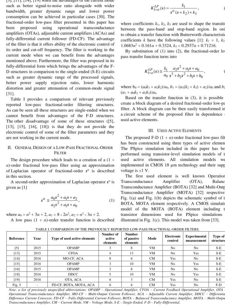
The first used element is well known Operational Transconductance Amplifier (OTA), Balanced Transconductance Amplifier (BOTA) [32] and Multi-Output Transconductance Amplifier (MOTA) [32] respectively. Fig. 1(a) and Fig. 1(b) depicts the schematic symbol of the BOTA, MOTA element respectively. A CMOS simulation model of the MOTA (BOTA) element including the transistor dimensions used for PSpice simulations is illustrated in Fig. 1(c). This model was taken from [33]. TABLE I. COMPARISON OF THE PREVIOUSLY REPORTED LOW-PASS FRACTIONAL-ORDER FILTERS.
Reference Year Type of used active elements
Number of active elements Number of passive elements Mode Electronic control Experimental measurement Type of structure [5] 2015 OPAMP 3 8 VM No No S-E
[13] 2015 CFOA 4 13 VM No Yes S-E
[14] 2016 MO-CF, ACA 8 6 CM Yes No S-E
[15] 2016 OPAMP 3 10 VM No Yes S-E
[16] 2015 OPAMP 3 8 VM No No S-E
[18] 2016 DDCC 5 10 VM No Yes S-E
[19] 2016 OTA, ACA 6 3 CM Yes No S-E
Fig. 5 - FD-CF, BOTA, MOTA, ACA 6 6 CM Yes No F-D
Note: a list of previously unspecified abbreviations: OPAMP – Operational Amplifier, CFOA – Current Feedback Operational Amplifier, OTA – Operational Transconductance Amplifier, MO-CF – Multi-Output Current Follower, ACA – Adjustable Current Amplifier, DDCC – Differential Difference Current Conveyor, FD-CF – Fully-Differential Current Follower, BOTA – Balanced Transconductance Amplifier, MOTA – Multi-Output Transconductance Amplifier, CM – Current Mode, VM – Voltage Mode, S-E – Single-Ended, F-D – Fully-Differential.
b) MOTA + -gm VIN+ V IN-IOUT+ I OUT-IOUT+ I OUT-BOTA + -gm vIN+ v IN-i OUT-iOUT+ a) Isetgm
IN- IN+ OUT+ OUT+ OUT-
OUT-VDD VSS M1 M2 M3 M4 M5 M6 M7 M8 M9 M10 M11 M12 M13 M14 M15 M16 M17 M18 10/0.36 10/0.36 10/0.36 10/0.36 10/0.36 10/0.36 10/0.36 10/0.36 10/0.36 10/0.36 10/0.36 10/0.36 10/0.36 10/0.36 10/0.36 10/0.36 10/0.36 10/0.36 c) Isetgm Isetgm
Fig. 1. Schematic symbol of the BOTA element (a); Schematic symbol of the MOTA element (b); Used transistor-level model of the MOTA (BOTA) element (c).
The relations between the input and output terminals of the MOTA (BOTA) element are described by: iOUT+ =
iOUT˗ = gm(vIN+ ˗ vIN˗), where gm is the transconductance of
this element. The transconductance of this particular implementation of the MOTA (BOTA) is controlled electronically by control current Isetgm.
The second used active element is Fully-Differential Current Follower (FD-CF) [34]. Its schematic symbol and CMOS simulation model including the transistor dimensions of this active element taken from [35] are shown in Fig. 2(a),
Fig. 2(b) respectively. Behavior of this active element is given by the following relations: iOUT1 = iOUT3 = (iIN+ ˗ iIN˗),
iOUT2 = iOUT4 = ˗ (iIN+ ˗ iIN˗).
The last used element is Adjustable Current Amplifier (ACA) [36]. This active element can be described by following relation: iOUT+ = − iOUT− = B · (iIN+ − iIN−), where
B is current gain of the ACA element. The current gain of the ACA element is controlled by control current IsetB in
this particular case. Figure 3 illustrates the schematic symbol and CMOS simulation model including the transistor dimensions [36] used for PSpice simulations.
a) + -iOUT1 iOUT2 iOUT3 iOUT4 iIN+ i IN-FD-CF
IN+ OUT1+ OUT2+ OUT1-
OUT2-VDD VSS 100µA M1 M2 M3 M4 M5 M6 M7 M8 M9 M10 M11 M12 M13 M14 M15 M16 M17 M19 M20 M 21M22 M23 M18 8/1 8/1 2/1 2/1 2/1 5/1 5/1 5/1 5/1 5/1 5/1 5/1 5/1 5/1 20/1 20/1 20/1 20/1 20/1 20/1 20/1 20/1 20/1 b)
IN-Fig. 2. Fully-Differential Current Follower: a) schematic symbol, b) used transistor-level model. a) B ACA
i
IN-i
OUT+i
OUT-i
IN+ + _I
setB b) M1 IN+ IN-100 mA 100 mA 50 mA 50 mA 50 mA 50 mA IsetB OUT-OUT+ M2 M3 M4 M5 M6 M7 M8 M9 M10 M11 M12 M13 M14 M15 M16 M17 M18 M19 M20 M21 M22 M23 M24 M25 M26 M27 M28 M29 M30 M31 M32 M33 M34 M35 M36 M37 M38 M39 M40 M41 M42 VSS VDD IsetB 10/0.54 10/0.54 10/0.54 10/0.54 10/0.54 10/0.54 10/0.54 10/0.54 30/0.54 30/0.54 30/0.54 30/0.54 30/0.54 30/0.54 30/0.54 30/0.54 37/0.54 37/0.54 37/0.54 37/0.54 37/0.54 37/0.54 37/0.54 37/0.54 111/0.54 111/0.54 111/0.54 111/0.54 111/0.54 111/0.54 111/0.54 111/0.54 37/0.9 37/0.9 37/0.9 37/0.9 37/0.9 10/0.9 10/0.9 10/0.9 10/0.9 10/0.9Fig. 3. Adjustable current amplifier: a) schematic symbol, b) used transistor-level model.
IV. DESCRIPTION OF THE PROPOSED FILTER
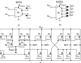
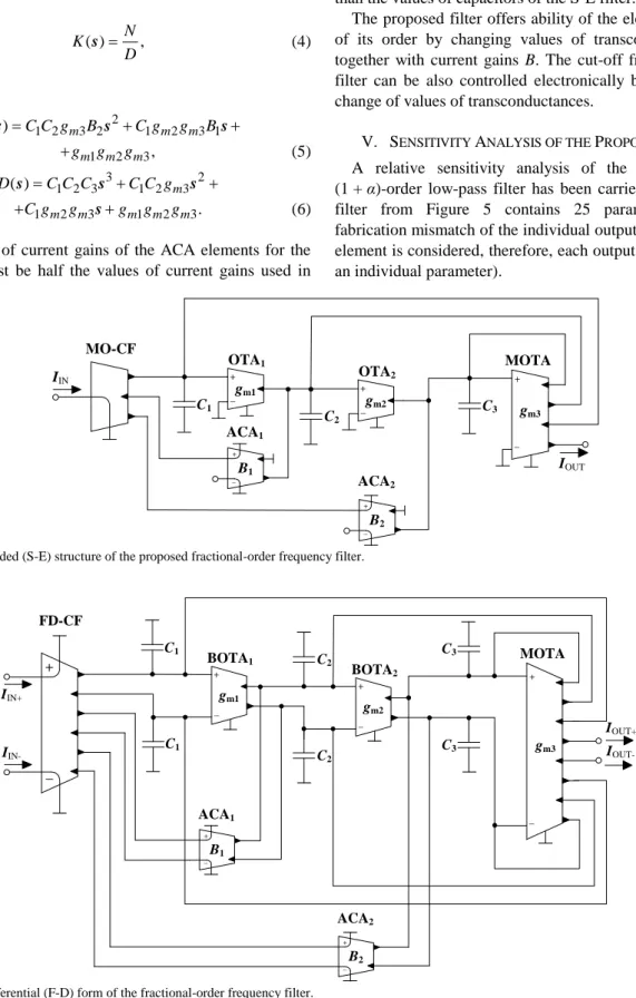
The presented filter is a fully-differential form of the S-E (1 + α)-order low-pass filter proposed in [37]. The F-D filter was obtained by transformation of its single-ended form (“mirroring” passive parts around horizontal plane of the
filter). The circuit structure of the S-E filter from [37] is shown in Fig. 4. It employs one MO-CF, three OTAs (two OTAs and one MOTA) and two ACAs. Figure 5 depicts the proposed F-D (1 + α)-order low-pass filter. It consists of one FD-CF, three OTA (two BOTAs and one MOTA) and two ACAs. Thus, the number of the used active elements in the
F-D structure stays the same as in case of the S-E filter from [37].
The transfer function of both S-E and F-D filter is given by ( ) N, K D s (4) where: 2 1 2 3 2 1 2 3 1 1 2 3 ( ) , m m m m m m N C C g B C g g B g g g s s s (5) 3 2 1 2 3 1 2 3 1 2 3 1 2 3 ( ) . m m m m m m D C C C C C g C g g g g g s s s s (6)
The values of current gains of the ACA elements for the F-D filter must be half the values of current gains used in
case of the S-E filter in order to obtain the same transfer functions for both S-E and F-D filter. The values of capacitors used for the F-D filter must be two-times higher than the values of capacitors of the S-E filter.
The proposed filter offers ability of the electronic control of its order by changing values of transconductances gm
together with current gains B. The cut-off frequency of the filter can be also controlled electronically by simultaneous change of values of transconductances.
V. SENSITIVITY ANALYSIS OF THE PROPOSED FILTER A relative sensitivity analysis of the presented F-D (1 + α)-order low-pass filter has been carried out. The F-D filter from Figure 5 contains 25 parameters (certain fabrication mismatch of the individual outputs of each active element is considered, therefore, each output is presented by an individual parameter). OTA1 gm1 C1 C2 C3 + _ + _ OTA2 gm2 + _ MOTA MO-CF IOUT IIN gm3 ACA1 B1 + _ ACA 2 B2 + _
Fig. 4. Single-Ended (S-E) structure of the proposed fractional-order frequency filter.
BOTA1 gm1 C1 C2 C3 + _ + _ MOTA FD-CF IOUT+ IIN- gm3 ACA1 B1 + _ ACA2 B2 + _ IIN+ + _ BOTA2 gm2 + _ C1 C3 IOUT-C2
Fig. 5. Fully-Differential (F-D) form of the fractional-order frequency filter. The considered parameters are: C1, C2, C3, gm11, gm12,
gm21, gm22, gm31, gm32, gm33, gm34, gm35, gm36, gm37, gm38, n1, n2,
n3, n4, n5, n6, B11, B12, B21, B22) where gm11, gm12, gm21, gm22,
gm31, gm32, gm33, gm34, gm35, gm36, gm37, gm38 are
transconductances of individual outputs of BOTA1, BOTA2
and MOTA elements, n1, n2, n3, n4, n5, n6 are transfers of
individual outputs of the FD-CF element and B11, B12, B21,
B22 are current gains of individual outputs of the ACA
elements.
The change of any of these parameters can significantly influence the characteristics of the filter. When taking all these parameters into consideration, the denominator of the
presented F-D filter turns into 3 2 3 2 1 0 ( ) , real D s s d s d sd d (7) where: 3 64 1 2 3, d C C C (8) 2 32 1 2 m31 32 1 2 m38, d C C g C C g (9) 1 21 32 1 22 37 1 21 37 1 22 32 1 16 16 16 16 , m m m m m m m m d g g C g g C g g C g g C (10) 0 11 21 33 11 21 36 11 22 33 11 22 36 12 21 33 12 21 36 12 22 33 12 22 36 8 8 8 8 8 8 8 8 . m m m m m m m m m m m m m m m m m m m m m m m m d g g g g g g g g g g g g g g g g g g g g g g g g (11)
The numerator takes a form of 2 2 1 0 ( ) , real N s s e se e (12) where: 2 22 6 34 1 2 22 5 34 1 2 21 5 34 1 2 21 6 34 1 2 16 16 16 16 , m m m m e B n g C C B n g C C B n g C C B n g C C (13) 1 12 3 21 34 1 12 3 22 34 1 11 3 22 34 1 12 4 21 34 1 11 4 21 34 1 11 4 22 34 1 11 3 21 34 1 12 4 22 34 1 8 8 8 8 8 8 8 , m m m m m m m m m m m m m m m m e B n g g C B n g g C B n g g C B n g g C B n g g C B n g g C B n g g C B n g g C (14) 0 1 11 21 34 1 11 22 34 1 12 21 34 1 12 22 34 2 11 21 34 2 11 22 34 2 12 21 34 2 12 22 34 8 8 8 8 8 8 8 8 . m m m m m m m m m m m m m m m m m m m m m m m m e n g g g n g g g n g g g n g g g n g g g n g g g n g g g n g g g (15)
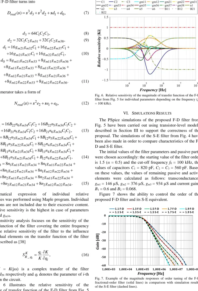
Mathematical expression of individual relative sensitivities was performed using Maple program. Individual calculations are not included due to their excessive content. The relative sensitivity is the highest in case of parameters C2, C3 and gm34.
The sensitivity analysis focuses on the sensitivity of the transfer function of the filter covering the entire frequency band. The relative sensitivity of the filter to the influence of individual elements on the transfer function of the filter can be described as [38] _ i , K i R q i q K S K q (16)
where K = K(jω) is a complex transfer of the filter K = IOUT/IIN respectively and qi denotes the parameter of i-th
element in the circuit.
Figure 6 illustrates the relative sensitivity of the magnitude of transfer function of the F-D filter from Fig. 5 to the given parameters of the filter. It can be seen that the individual relative sensitivities have typical values (up to 1). These sensitivities were taken into consideration during the proposal.
Fig. 6. Relative sensitivity of the magnitude of transfer function of the F-D filter from Fig. 5 for individual parameters depending on the frequency (f0 = 100 kHz).
VI. SIMULATIONS RESULTS
The PSpice simulations of the proposed F-D filter from Fig. 5 have been carried out using transistor-level models described in Section III to support the correctness of the proposal. The simulations of the S-E filter from Fig. 4 have been also made in order to compare characteristics of the F-D and S-E filter.
The initial values of the filter parameters and passive parts were chosen accordingly: the starting value of the filter order is 1.5 (α = 0.5) and the cut-off frequency f0 = 100 kHz, the
values of capacitors C1 = 820 pF, C2 = C3 = 560 pF. Based
on these values, the values of remaining passive and active elements were calculated as follows: transconductances gm1 = 146 µS, gm2 = 376 µS, gm3 = 934 µS and current gains
B1 = 0.6 and B2 = 0.068.
Figure 7 shows the ability to control the order of the proposed F-D filter and its S-E equivalent.
-60 -50 -40 -30 -20 -10 0
1,00E+03 1,00E+04 1,00E+05 1,00E+06 1,00E+07 1,00E+08
G ai n [d B ] Frequency[Hz] 1.1 F-D 1.3 F-D 1.5 F-D 1.7 F-D 1.9 F-D
1.1 S-E 1.3 S-E 1.5 S-E 1.7 S-E 1.9 S-E
Fig. 7. Example of the magnitude responses of order tuning of the F-D fractional-order filter (solid lines) in comparison with simulation results of the S-E filter (dashed lines).
The order can be controlled electronically by changing values of individual transconductances gm and current gains
B. This was tested for five different values of parameter α (0.1, 0.3, 0.5, 0.7, 0.9) when the cut-off frequency was 100
kHz. The calculated values of used passive parts, transconductances and current gains for chosen values of parameter α are summarized in Table II. The values of transconductances are the same for both S-E and F-D filter. The values of capacitors and current gains of the S-E filter are given before the slash and the values of capacitors and current gains in case of the F-D filter are given after the slash in Table II.
TABLE II. USED VALUES OF PARAMETERS C, GM AND B FOR SELECTED ALPHA. VALUES FOR S-E / F-D CONFIGURATION
OF THE FILTER. α [-] 0.1 0.3 0.5 0.7 0.9 C1 [pF] 820/1640 C2 = C3 [pF] 560/1120 gm1 [µS] 112 133 147 174 210 gm2 [µS] 340 370 370 417 417 gm3 [µS] 1499 1181 909 909 954 B1 [-] 0.760/ 0.380 0.700/ 0.350 0.610/ 0.305 0.515/ 0.258 0.428/ 0.214 B2 [-] 0.170/ 0.085 0.117/ 0.059 0.070/ 0.035 0.033/ 0.017 0.008/ 0.004 The slope of attenuation for selected values of α, obtained from the simulations of the proposed F-D filter (colored solid lines) and simulations of its S-E equivalent (black dashed lines) are compared in Table III. It can be seen that the values of the slope of attenuation obtained from the proposed F-D filter are usually slightly higher and closer to the theoretical expectations than the values obtained from the S-E filter.
TABLE III. THEORETICAL AND SIMULATED VALUES OF THE SLOPE OF ATTENUATION WHEN CHANGING THE ORDER.
α [-] 0.1 0.3 0.5 0.7 0.9
Theoretical slope of
attenuation [dB/dec] 22.0 26.0 30.0 34.0 38.0 Simulated S-E slope of
attenuation [dB/dec] 20.8 25.5 30.3 34.5 36.7 Simulated F-D slope of
attenuation [dB/dec] 21.2 26.0 30.6 34.4 37.1
Figure 8 illustrates simulated phase responses of transfer functions of the proposed F-D filter (colored solid lines) and simulations of its S-E equivalent (black dashed lines) from Fig. 7. It can be seen that the phase responses correspond with the particular order. For example, the phase response of 1.1 order ends around 90 degrees, or the phase response of 1.9 order is getting close to 170 degrees etc.
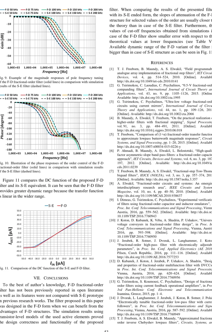
The ability to control the cut-off frequency of the proposed F-D filter and its S-E equivalent is depicted in Fig. 9. The cut-off frequency can be controlled electronically without disturbing the desired order by changing values of transconductances gm when maintaining current gains B
unchanged. This ability has been tested for 5 different cut-off frequencies (50 kHz, 75 kHz, 100 kHz, 150 kHz and 200 kHz) when the order of the filter was set to 1.5. Table IV summarizes the calculated values of used passive parts, transconductances and current gains for chosen values cut-off frequencies. The values of transconductances are
again the same for both S-E and F-D filter. The values of capacitors and current gains of the S-E filter are given before the slash and the values of capacitors and current gains in case of the F-D filter are given after the slash.
-180 -160 -140 -120 -100 -80 -60 -40 -20 0
1,00E+03 1,00E+04 1,00E+05 1,00E+06 1,00E+07 1,00E+08
Ph ase [d egr ee ] Frequency[Hz] 1.1 F-D 1.3 F-D 1.5 F-D 1.7 F-D 1.9 F-D
1.1 S-E 1.3 S-E 1.5 S-E 1.7 S-E 1.9 S-E
Fig. 8. Illustration of the phase responses of the order control of the F-D fractional-order filter (solid lines) in comparison with simulation results of the S-E filter (dashed lines).
TABLE IV. USED VALUES OF PARAMETERS C, GM AND B FOR SELECTED F0 WHEN ALPHA = 0.5. VALUES FOR S-E / F-D
CONFIGURATION OF THE FILTER. Theoretical pole frequency [kHz] 50 75 100 150 200 C1 [pF] 820/1640 C2 = C3 [pF] 560/1120 gm1 [µS] 74 110 147 220 294 gm2 [µS] 182 278 370 556 769 gm3 [µS] 465 667 909 1333 1818 B1 [-] 0.610/0.305 B2 [-] 0.070/0.035
The obtained values of the cut-off frequency from the simulations of the proposed F-D filter (colored solid lines) and simulations of its S-E equivalent (black dashed lines) can be compared in Table V. The obtained values show that the pole frequency of the proposed F-D filter is closer to the theory at lower frequencies than the values of the cut-off frequency of the corresponding S-E filter. The cut-off frequency of the F-D filter is at higher frequencies higher than the expected values and the difference is more significant as the frequency increases.
The phase responses corresponding with the transfer functions of the proposed F-D filter (colored solid lines) and simulations of its S-E equivalent (black dashed lines) from Fig. 9 are shown in Fig. 10. The largest differences between the responses of the S-E and F-D filter can be seen at higher frequencies.
TABLE V. THEORETICAL AND SIMULATED VALUES OF THE CUT-OFF FREQUENCY WHEN THE ORDER EQUALS 1.5.
f0 [kHz] 50 75 100 150 200
Simulated S-E
cut-off frequency [kHz] 52.1 78.9 102.4 151.4 201.3 Simulated F-D
-60 -50 -40 -30 -20 -10 0
1,00E+03 1,00E+04 1,00E+05 1,00E+06 1,00E+07 1,00E+08
G ai n [dB ] Frequency[Hz] F-D 50 kHz F-D 75 kHz F-D 100 kHz F-D 150 kHz F-D 200 kHz
S-E 50 kHz S-E 75 kHz S-E 100 kHz S-E 150 kHz S-E 200 kHz
Fig. 9. Example of the magnitude responses of pole frequency tuning of the F-D fractional-order filter (solid lines) in comparison with simulation results of the S-E filter (dashed lines).
-180 -160 -140 -120 -100 -80 -60 -40 -20 0
1,00E+03 1,00E+04 1,00E+05 1,00E+06 1,00E+07 1,00E+08
Ph as e [de gr ee ] Frequency[Hz] F-D 50 kHz F-D 75 kHz F-D 100 kHz F-D 150 kHz F-D 200 kHz
S-E 50 kHz S-E 75 kHz S-E 100 kHz S-E 150 kHz S-E 200 kHz
Fig. 10. Illustration of the phase responses of the order control of the F-D fractional-order filter (solid lines) in comparison with simulation results of the S-E filter (dashed lines).
Figure 11 compares the DC function of the proposed F-D filter and its S-E equivalent. It can be seen that the F-D filter provides greater dynamic range because the transfer function is linear in the wider range.
-50.0 -40.0 -30.0 -20.0 -10.0 0.0 10.0 20.0 30.0 40.0 50.0 -50.0 -40.0 -30.0 -20.0 -10.0 0.0 10.0 20.0 30.0 40.0 50.0 IOUT [μ A] IIN[μA] S-E F-D
Fig. 11. Comparison of the DC function of the S-E and F-D filter. VII. CONCLUSIONS
To the best of author’s knowledge, F-D fractional-order filter has not been previously reported in open literature as well as its features were not compared with S-E prototype in previous research works. The filter proposed in this paper was designed in the F-D form when we can benefit from the advantages of F-D structures. The simulation results using transistor-level models of the used active elements proved the design correctness and functionality of the proposed
filter. When comparing the results of the presented filter with its S-E ended form, the slopes of attenuation of the F-D structure for selected values of the order are usually closer to the theory than in case of the S-E filter. Furthermore, the values of cut-off frequencies obtained from simulations in case of the F-D filter show smaller error with respect to the theoretical values at lower frequencies (see Table V). Available dynamic range of the F-D variant of the filter is bigger than in case of S-E structure as can be seen in Fig. 11.
REFERENCES
[1] T. J. Freeborn, B. Maundy, A. S. Elwakil, “Field programmable analogue array implementation of fractional step filters”, IET Circuits Devices, vol. 4, pp. 514–524, 2010. [Online]. Available: http://dx.doi.org/10.1049/iet-cds.2010.0141
[2] G. Tsirimokou, C. Laoudias, C. Psychalinos, “0.5-V fractional-order companding filters”, International Journal of Circuit Theory and Applications, vol. 43, no. 9, pp. 1105–1126, 2015. [Online]. Available: http://dx.doi.org/10.1002/cta.1995
[3] G. Tsirimokou, C. Psychalinos, “Ultra-low voltage fractional-order circuits using current mirrors”, International Journal of Circuit Theory and Applications, vol. 44, no. 1, pp. 109–126, 2016. [Online]. Available: http://dx.doi.org/10.1002/cta.2066
[4] B. Maundy, A. Elwakil, T. Freeborn, “On the practical realization of higher-order filters with fractional stepping”, Signal Processing, vol. 91, no. 3, pp. 484–491, 2011. [Online]. Available: http://dx.doi.org/10.1016/j.sigpro.2010.06.018
[5] T. Freeborn, “Comparison of (1+α) fractional-order transfer functions to approximate lowpass butterworth magnitude responses”, Circuits, Systems, and Signal Processing, pp. 1–20, 2015. [Online]. Available: http://dx.doi.org/10.1007/s00034-015-0226-y
[6] P. Ahmadi, B. Maundy, A. Elwakil, L. Belostotski, “High-quality factor asymmetric-slope band-pass filters: a fractional-order capacitor approach”, IET Circuits, Devices and Systems, vol. 6, no. 3, pp. 187– 197, 2012. [Online]. Available: http://dx.doi.org/10.1049/iet-cds.2011.0239
[7] T. Freeborn, B. Maundy, A. S. Elwakil, “Fractional-step Tow-Thomas biquad filters”, IEICE (NOLTA), vol. 3, no. 3, pp. 357–374, 2012. [Online]. Available: http://dx.doi.org/10.1587/nolta.3.357
[8] A. Elwakil, “Fractional-order circuits and systems: An emerging interdisciplinary research area”, IEEE Circuits and Systems Magazine, vol. 10, no. 4, pp. 40–50, 2010. [Online]. Available: http://dx.doi.org/10.1109/MCAS.2010.938637
[9] I. Dimeas, G. Tsirimokou, C. Psychalinos, “Experimental verification of filters using fractional-order capacitor and inductor emulators”, in
Proc. Int. Conf. Telecommunications and Signal Processing, Vienna, Austria, 2016, pp. 559–562. [Online]. Available: http://dx.doi.org/ 10.1109/TSP.2016.7760943
[10] J. Koton, D. Kubanek, K. Vrba, A. Shadrin, P. Ushakov, “Universal voltage conveyors in fractional-order filter design”, in Proc. Int. Conf. Telecommunications and Signal Processing, Vienna, Austria, 2016, pp. 593–598. [Online]. Available: http://dx.doi.org/ 10.1109/TSP.2016.7760950
[11] J. Jerabek, R. Sotner, J. Dvorak, L. Langhammer, J. Koton, “Fractional-order high-pass filter with electronically adjustable parameters”, in Proc. Int. Conf. Applied Electronics (AE 2016),
Pilsen, Czech Republic, 2016, pp. 111–116. [Online]. Available: http://dx.doi.org/10.1109/AE.2016.7577253
[12] D. Kubanek, J. Koton, J. Jerabek, P. Ushakov, A. Shadrin, “Design and properties of fractional-order multifunction filter with DVCCs”, in Proc. Int. Conf. Telecommunications and Signal Processing, Vienna, Austria, 2016, pp. 620–624. [Online]. Available: http://dx.doi.org/10.1109/TSP.2016.7760956
[13] G. Tsirimokou, S. Koumousi, C. Psychalinos, “Design of fractional-order filters using current feedback operational amplifiers”, in Proc. 3rd Pan-Hellenic Conf. Electronic and Telecommunications, Ioannina, Greece, 2015, pp. 1–4.
[14] J. Dvorak, L. Langhammer, J. Jerabek, J. Koton, R. Sotner, J. Polak, “Electronically tunable fractional-order low-pass filter with current followers”, in Proc. Int. Conf. Telecommunications and Signal Processing, Vienna, Austria, 2016, pp. 587–592. [Online]. Available: http://dx.doi.org/10.1109/TSP.2016.7760949
[15] T. J. Freeborn, A. S. Elwakil, B. Maundy, “Approximated fractional-order inverse Chebyshev lowpass filters”, Circuits, Systems, and
Signal Processing, vol. 35, pp. 1973–1982, 2016. [Online]. Available: http://dx.doi.org/10.1007/s00034-015-0222-2
[16] T. Freeborn, B. Maundy, A. Elwakil, “Approximated fractional order Chebyshev lowpass filters”, Mathematical Problems in Engineering, vol. 2015, pp. 1–7, 2015. [Online]. Available: http://dx.doi.org/ 10.1155/2015/832468
[17] L. A. Said, A. G. Radwan, A. H. Madian, A. M. Soliman, “Fractional-order inverting and non-inverting filters based on CFOA”, in Proc. Int. Conf. Telecommunications and Signal Processing, Vienna, Austria, 2016, pp. 599–602. [Online]. Available: http://dx.doi.org/10.1109/TSP.2016.7760951
[18] F. Khateb, D. Kubnek, G. Tsirimokou, C. Psychalinos, “Fractional-order filters based on low-voltage DDCCs”, Microelectronics Journal, vol. 50, pp. 50–59, 2016. [Online]. Available: http://dx.doi.org/10.1016/j.mejo.2016.02.002
[19] J. Jerabek, R. Sotner, D. Kubnek, J. Dvorak, L. Langhammer, N. Herencsar, K. Vrba, “Fractional-order low-pass filter with electronically adjustable parameters”, in Proc. Int. Conf. Telecommunications and Signal Processing, Vienna, Austria, 2016, pp. 569–574. [Online]. Available: http://dx.doi.org/10.1109/TSP. 2016.7760945
[20] M. E. Fouda, A. Soltan, A. G. Radwan, A. M. Soliman, “Fractional-order multi-phase oscillators design and analysis suitable for higher-order PSK applications”, Analog Integrated Circuits and Signal Processing, vol. 87, pp. 301–312, 2016. [Online]. Available: http://dx.doi.org/10.1007/s10470-016-0716-2
[21] A. G. Radwan, A. M. Soliman, A. S. Elwakil, “Fractional-order sinusoidal oscillators: Four practical circuit design examples”,
International Journal of Circuit Theory and Applications,vol. 36, pp. 473–492, 2008. [Online]. Available: http://dx.doi.org/10.1109/ ICM.2007.4497668
[22] A. G. Radwan, A. S. Elwakil, A. M. Soliman, “Fractional-order sinusoidal oscillators: Design procedure and practical examples”,
IEEE Trans. Circuits and Systems I: Regular Papers, vol. 55, pp. 2051–2063, 2008. [Online]. Available: http://dx.doi.org/10.1109/ TCSI.2008.918196
[23] I. Podlubny, I. Petras, B. M. Vinagre, P. O'Leary, L. Dorcak, “Analogue realizations of fractional-order controllers”, Nonlinear Dynamics, vol. 29, no. 1, pp. 281–296, 2002. [Online]. Available: http://dx.doi.org/10.1023/A:1016556604320
[24] T. Freeborn, “A Survey of fractional-order circuit models for biology and biomedicine”, IEEE Circuits and Systems Magazine, vol. 3, no. 3, pp. 416–424, 2013. [Online]. Available: http://dx.doi.org/ 10.1109/JETCAS.2013.2265797
[25] T. Freeborn, B. Maundy, A. Elwakil, “Extracting the parameters of the double-dispersion Cole bioimpedance model from magnitude response measurements”, Medical & Biological Engineering & Computing, vol. 52, pp. 749–758, 2014. [Online]. Available: http://dx.doi.org/10.1007/s11517-014-1175-5
[26] T. Freeborn, B. Maundy, A. Elwakil, “Cole impedance extractions from the step-response of a current excited fruit sample”, Computers
and Electronics in Agriculture, vol. 98, pp. 100–108, 2013. [Online]. Available: http://dx.doi.org/10.1016/j.compag.2013.07.017
[27] T. Haba, G. Loum, J. Zoueu, G. Ablart, “Use of a component with fractional impedance in the realization of an analogical regulator of order ½”, Journal of Applied Sciences, vol. 8, pp. 59–67, 2008. [Online]. Available: http://dx.doi.org/10.3923/jas.2008.59.67 [28] M. Sivarama Krishna, S. Das, K. Biswas, B. Goswami, “Fabrication
of a fractional order capacitor with desired specifications: a study on process identification and characterization”, IEEE Trans. Electron Devices, vol. 58, pp. 4067–4073, 2011. [Online]. Available: http://dx.doi.org/10.1109/TED.2011.2166763
[29] D. Mondal, K. Biswas, “Performance study of fractional order integrator using single-component fractional order element”, IET Circuits, Devices & Systems, vol. 5, no. 4, pp. 334–342, 2011. [Online]. Available: http://dx.doi.org/10.1049/iet-cds.2010.0366 [30] C. Toumazou, F. J. Lidgey, D. G. Haigh, Analog IC design: the
current-mode approach. London: Institution of Electrical Engineers, 1996.
[31] J. Jerabek, K. Vrba, “Comparison of the fully-differential and single-ended solutions of the frequency filter with current followers and adjustable current amplifier”, in Proc. the Eleventh Int. Conf. Networks (ICN2012), France, 2012, pp. 50–54.
[32] J. Jerabek, K. Vrba, “Current-mode tunable and adjustable filter with digitally adjustable current amplifier and transconductance amplifiers”, in Proc. European Conf. Circuits Technology and Devices (ECCTD 2010), Spain, 2010, pp. 101–104.
[33] R. Sotner, N. Herencsar, J. Jerabek, R. Prokop, A. Kartci, T. Dostal, K. Vrba, “Z-Copy controlled-gain voltage differencing current conveyor: advanced possibilities in direct electronic control of first-order filter”, Elektronika ir Elektrotechnika, vol. 20, pp. 77–83, 2014. [Online]. Available: http://dx.doi.org/10.5755/j01.eee.20.6. 7272
[34] J. Jerabek, K. Vrba, “Fully differential universal filter with differential and adjustable current followers and transconductance amplifiers”, in Proc. Int. Conf. Telecommunications and Signal Processing, Hungary, 2010, pp. 5–9.
[35] J. Jerabek, R. Sotner, K. Vrba, “Electronically adjustable triple-input single-output filter with voltage differencing transconductance amplifier”, Revue Roumaine des Sciences Techniques - Serie Electrotechnique et Energetique, vol. 59, pp. 163–172, 2015. [36] J. Jerabek, J. Koton, R. Sotner, K. Vrba, “Adjustable band-pass filter
with current active elements: two fully-differential and single-ended solutions”, Analog integrated circuits and signal processing, vol. 74, pp. 129–139, 2013. [Online]. Available: http://dx.doi.org/ 10.1007/s10470-012-9942-4
[37] L. Langhammer, J. Dvorak, J. Jerabek, J. Koton, “Fractional-order low-pass filter with electronic tunability of its order and cut-off frequency”, Int. Journal of Electronics and Communications AEÜ, (Submitted for review).
[38] W. -K. Chen, The circuits and filters handbook. USA: CRC Press, 2009.