An Optimization Design Strategy for
Arithmetic Logic Unit
Jitesh R. Shinde1,*, Shilpa J. Shinde2
1Department of Electronics and Communication Engineering, Vaagdevi College of Engineering, India
2M.Tech in Electronics Engineering, Nagpur, India
Copyright©2019 by authors, all rights reserved. Authors agree that this article remains permanently open access under the terms of the Creative Commons Attribution License 4.0 International License
Abstract
The work in this paper presents a step by step optimization approach for the Arithmetic Logic Unit (ALU) at the logic circuit level. Herein concept of resource sharing (viz. operator sharing, functionality sharing), the concept of optimized arithmetic expressions (viz. arranging expression trees for minimum delay, sharing common subexpression, merging cascaded adders with carry) for optimization of combinational blocks in ALU had been used.The work in this paper shows how a simple tools like Deeds Digital Circuit Simulator (open source) or Aldec’s Active HDL in combination with synthesis tool which can be used as effective teaching resource to teach concept of digital circuit design and thereby provides a vision to beginners how to start with VLSI project in VLSI digital domain and make it to a successful end.Keywords Arithmetic Unit, Logical Unit, Arithmetic
Logical Unit (ALU), Resource Sharing, Operator Sharing1. Introduction
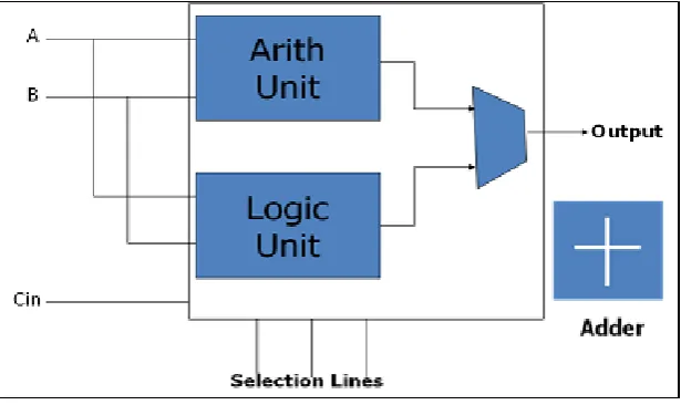
An arithmetic logic unit (ALU) is a combination of various digital circuits merged together to execute data processing instruction (i.e. arithmetic & logical) in the central processing unit (CPU) of any processor or microcontroller or computer. ALU is basically a multi-function combinational digital logic circuit which requires one or two operands upon which it operates and produces the result.
The timing response of ALU depends on complexity & manner in which the circuit is designed. There are various ways by which the circuit in HDL (Hardware Description Language) can be implemented. Some such ways are resource sharing & optimized arithmetic expressions.
Resource sharing diminishes the amount of hardware required to implement HDL operations. Without resource sharing, each HDL operation is built with separate circuitry. For example, every ‘+’ with noncomputable operands
causes a new adder to be built. This repetition of hardware increases the area of design. In contrast, with resource sharing, several VHDL + operations can be implemented with a single adder to reduce the amount of hardware required. Also, different operations such as ‘+’ and ‘–’ can be assigned to a single adder or subtracter to reduce a design’s circuit area further [11, 12]. The resource sharing
techniques used in the optimization of the ALU in this paper are operator sharing & functionality sharing.
Operator sharing is a resource sharing technique to reduce the overall size of synthesized hardware. If the same operator is used in several different expressions, it can be shared. The sharing is done by routing the proper data to or from this particular operator via multiplexing circuits. Operators can be shared in mutually exclusive branches by proper routing of the input operands and/ or result. It is more beneficial for complex operators. The merit of sharing and the degree of saving depend on the relative complexity of the multiplexing circuit and the operator. However, sharing normally faces evaluation of the Boolean expressions and evaluations of the operators in cascade and this may introduce extra propagation delay.
Functionality sharing is a resource sharing technique. In a large, complex digital system, such as a processor, an array of functions is needed. Some functions or operations may be interlinked or may have some common functionality. If such common functions are implemented by a common circuit, then the approach is referred as functionality sharing. Example of functionality sharing can be an implementation of subtractor block using adder block using the concept of 2’s complement arithmetic [1, 2].
Optimized Arithmetic Expressions methodology uses the properties of arithmetic operators (such as commutative & associative properties of addition) to rearrange an expression so that it results in an optimized implementation. The three forms of arithmetic optimizations are arranging expression trees for minimum delay, merging cascaded adders with a carry, sharing common sub-expressions [1].
building blocks are there in the circuit to execute the given instructions [2]. The basics of ALU design are available in
the literature mentioned in the references [3, 4, 5, 6, 7 & 8].
Basically, an ALU should be capable of executing following arithmetic & logical functions as listed in tables 2.1 & 2.2.
The tables 2.2 suggests that one logical block having some logical gates (four) with 4:1 multiplexer will be required to implement logical operations AND, OR, XOR and NOT in ALU to get an output of logical block.
The table 1.2 suggests that one arithmetic block consisting of 8 instances of one-bit full adder block with two 8:1 multiplexer will be required to implement operations Addition, Subtraction, Increment, Decrement and Passing of Input signal and thereby getting an output of
In addition to this, one 2:1 multiplexer will also be required to decide at given instance of time whether ALU is implementing arithmetic or logical function. If select bit ‘Si’ (S3 in figure 2.1) of multiplexer equals to‘1’, then ALU will perform logical operation otherwise it will perform arithmetic operations.
Thus, combinational digital blocks to implement an ALU in traditional approach are two 8:1 multiplexer, one 2:1 multiplexer, 8 one-bit full adder block & 4 two-input logic gates, two NOT gates along with some constants (logic high or logic low) to get final output ‘Y’ of one bit ALU.
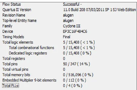
The logical circuit diagram was implemented in Deeds circuit simulator & using Aldec’s Active HDL tool with Altera’s (Intel) Quartus synthesis tool.
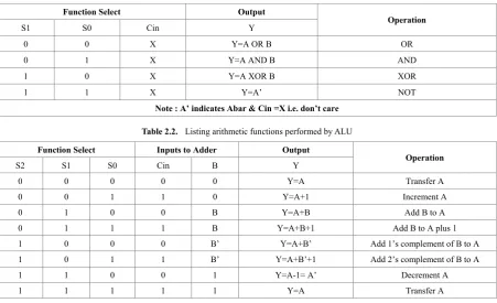
Table 2.1. Listing logical operations performed by ALU
Function Select Output
Operation
S1 S0 Cin Y
0 0 X Y=A OR B OR
0 1 X Y=A AND B AND
1 0 X Y=A XOR B XOR
1 1 X Y=A’ NOT
Note : A’ indicates Abar & Cin =X i.e. don’t care
Table 2.2. Listing arithmetic functions performed by ALU
Function Select Inputs to Adder Output
Operation
S2 S1 S0 Cin B Y
0 0 0 0 0 Y=A Transfer A
0 0 1 1 0 Y=A+1 Increment A
0 1 0 0 B Y=A+B Add B to A
0 1 1 1 B Y=A+B+1 Add B to A plus 1
1 0 0 0 B’ Y=A+B’ Add 1’s complement of B to A
1 0 1 1 B’ Y=A+B’+1 Add 2’s complement of B to A
1 1 0 0 1 Y=A-1= A’ Decrement A
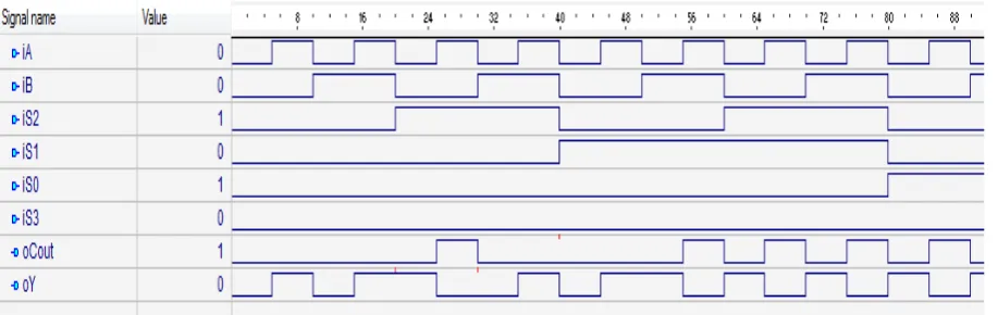
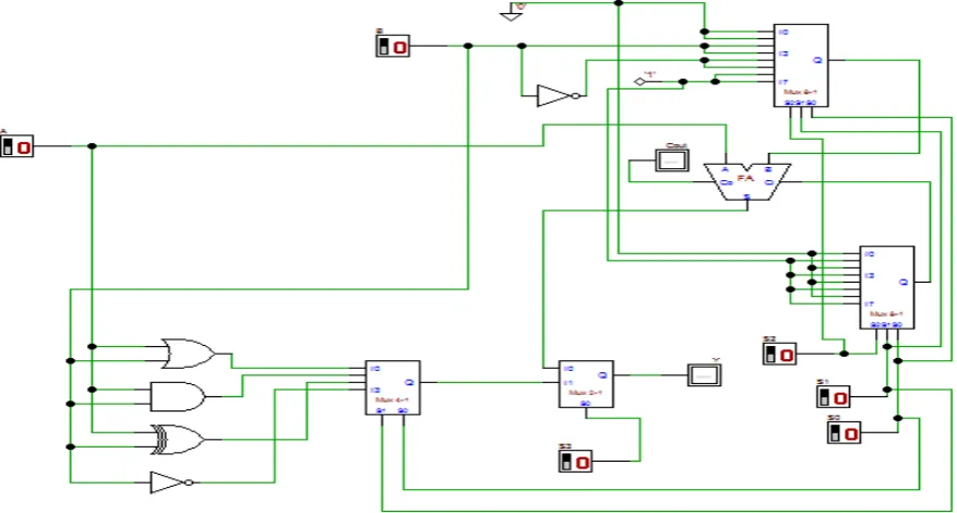
[image:2.595.73.525.416.691.2]Figure 2.1. Circuit schematic of 1-bit ALU (Deeds DCS)
[image:3.595.72.526.343.642.2]Figure 2.3. Propagation delay summary of entity ‘alugen’ (delay in nsec)
Figure 2.4. Power consumption of entity ‘alugen’
[image:4.595.72.531.504.649.2]3. ALU Design & Implementation:
Type II
Herein this approach, the concept of resource & operator sharing had been used to optimize the ALU. Herein, only one full adder block had been used to implement arithmetic operations given in table 2.1. The input logic for input terminal carry-in of full adder (as per table 2.2) is decided
[image:5.595.79.518.191.426.2]by 8:1 multiplexer i.e. for example: for S2S1S0= “000”, carry-in of full adder block is connected to logic ‘0’. Similarly, the input logic for input terminal ‘B’ of full adder (as per table 2.1) is decided by 8:1 multiplexer i.e. for example: for S2S1S0= “000”, input terminal ‘B’ of full adder block is connected to logic ‘0’. Rest of the working of the circuit is same as discussed in previous section.
Figure 3.1. Circuit schematic of entity ‘alugenopt’
[image:5.595.127.472.460.694.2]Figure 3.3. Propagation delay summary of entity ‘alugenopt’ (delay in nsec)
Figure 3.4. Power consumption summary of entity ‘alugenopt’
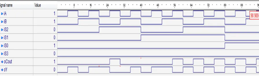
Figure 3.5. Output waveform of entity ‘alugenopt’
4. ALU Design & Implementation:
Type III
The general ALU architecture that can be inferred from section II is given in figure 4.1.
The strategy used in type III ALU optimization is based on the concept on resource sharing and concept of optimized arithmetic expressions.
In type III strategy, all arithmetic, as well as logical instructions are realized using one full adder block only.
The approach used in the realization of the final optimized logic circuit shown in figure 4.6 is illustrated with the help of figures from 4.1 to 4.5 and tables from 4.1 to 4.6 respectively.
Arithmetic Unit Realization
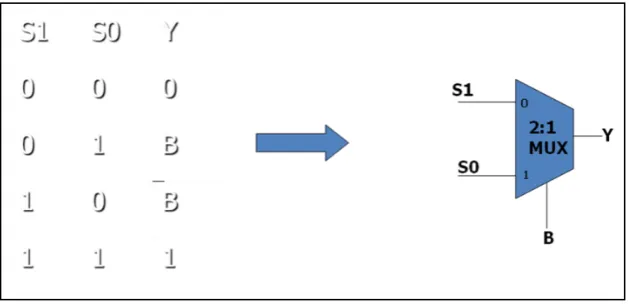
[image:6.595.127.473.82.242.2] [image:6.595.129.466.269.447.2] [image:6.595.75.524.475.609.2]decided. Finally, SOP (sum of product) logical equation for literal ‘Y’ in an optimized way is realized using 2:1 multiplexer (figure 4.4). The process is illustrated diagrammatically in figure 4.2, 4.3 and 4.4 respectively.
Logical Unit Realization
To find the equation for input literal ‘X’ of full adder block, first, the logic equation for literal ‘X’ for each gate is computed using the concept of K-map wherein SOP (sum of product) equation for literal ‘X’ has been computed as a function of literal viz. ‘A’ & ‘B’ respectively. This process had been illustrated in tables from 4.3 to 4.6 respectively
and then table 4.2 had been realized. Accordingly, the logical unit shown in figure 4.5 had been realized. The concept of K-map here used to find the logical equation for literal ‘X’ for corresponding gates & then final SOP (sum of product) equation for ‘X’ as shown in figure 4.5.
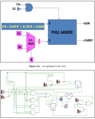
The final block diagram of an optimized 1-bit ALU is shown in figure 4.6.
[image:7.595.138.458.236.710.2]The logical circuit diagram implemented in Deeds DCS circuit simulator & waveform, flow summary, propagation delay report & power consumption analysis report obtained from Altera’s (Intel) Quartus tool are shown in figure 4.7 to 4.11 respectively.
Figure 4.1. Block diagram of 1 bit ALU
[image:7.595.145.453.245.428.2]Figure 4.3. Arithmetic unit logic in an optimized 1-bit ALU using 2:1 multiplexer
[image:8.595.139.456.252.441.2]Figure 4.4. Arithmetic unit logic in an optimized 1-bit ALU using 2:1 multiplexer
Table 4.1. Truth Table for Arithmetic Unit for an optimized 1-bit ALU
S2 S1 S0 Cin X Y Operation
0 0 0 0 A 0 Transfer A
0 0 0 1 A 0 Increment A
0 0 1 0 A B Add B to A
0 0 1 1 A B Add B to A plus 1
0 1 0 0 A B’ Add 1’s complement of B to A
0 1 0 1 A B’ Add 2’s complement of B to A
0 1 1 0 A 1 Decrement A
0 1 1 1 A 1 Transfer A
Table 4.2. Truth Table for Logical Unit
S2 S1 S0 Cin X Y Operation
1 0 0 x A+B 0 OR
1 0 1 x A’B B AND
1 1 0 x A’ B’ XOR
[image:8.595.69.527.477.709.2]Table 4.3. Truth Table for finding input ‘X’ for ORing operation i.e. X (A, B) = A +B
A B X Y=0 Operation
0 0 0 0 0
0 1 1 0 1
1 0 1 0 1
1 1 1 0 1
Table 4.4. Truth Table to find input ‘X’ for ANDing operation i.e. X (A, B) = A’ B
A B X Y=B Operation
0 0 0 0 0
0 1 1 1 0
1 0 0 0 0
1 1 0 1 1
Table 4.5. Truth Table to find input ‘X’ for XORing operation i.e. X (A, B) = A’
A B X Y=B’ Operation
0 0 1 1 0
0 1 1 0 1
1 0 0 1 1
[image:9.595.82.525.418.686.2]1 1 0 0 0
Table 4.6. Truth Table to find input ‘X’ for NOT operation i.e. X (A, B) = B
A B X Y=1 Operation
0 0 0 1 1
0 1 1 1 0
1 0 0 1 1
1 1 1 1 0
Figure 4.6. An optimized 1-bit ALU
Figure 4.7. Circuit schematic of 1 bit optimized ALU ‘aluopt’
[image:10.595.142.456.493.731.2]Figure 4.9. Propagation Delay Summary of 1 bit ALU implemented on Intel /Altera DE0 (Quartus 2)
Figure 4.10. Power consumption summary of 1 bit ALU implemented on Intel /Altera DE0 (Quartus 2)
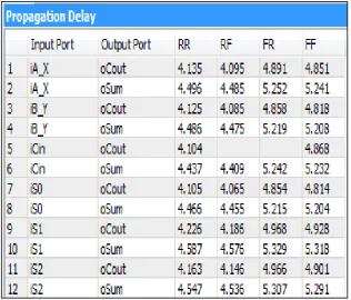
[image:11.595.139.455.375.540.2] [image:11.595.69.527.567.697.2]‘aluopt’. The highest propagation delay in ‘alugen’ is 6.12 nsec; in ‘alugenopt’ is 6.273 nsec while in ‘aluopt’ is 8.270 nsec.
The power analyzer summary comparison (figure 2.4, 3.4 & 4.10) shows considerable power savings in ‘aluopt’ in comparison to ‘alugen’ can be obtained. The power readings obtained here depend on input test vector combination taken.
[image:12.595.63.289.365.473.2]No benchmark work with similar formal specification of one-bit ALU is available. So, comparison of design strategy suggested in this paper cannot be done.
Table 5.1. Power comparison of ALU (Power in milliWatt)
Entity Name ALUgen ALUGen opt Aluopt
Total Thermal Power
Dissipation 105.42 101.46 103.99
Core Dynamic Thermal Power
Dissipation 0.76 0.63 0.37
Core Static Thermal
Power Dissipation 51.8 51.8 51.8
I/O Thermal Power
Dissipation 52.85 49.04 51.82
6. Conclusions
The empirical measurements quantifying the gap between VLSI implementation of ‘alugen’, ‘alugenopt’ & ‘aluopt’ has been presented in this paper.
In ‘alugen’ entity no concept of resource sharing had been used. Hence, for each corresponding arithmetic instruction execution in ALU block, one full adder block is required. On other hand in entities ‘alugenopt’ and ‘aluopt’ because of concept of resource sharing i.e. operator sharing and functionality sharing only one full adder block along with few multiplexer is required for implementation of arithmetic instruction in ALU.
Moreover, due to use of concept of optimized arithmetic expressions (viz. arranging expression trees for minimum delay, sharing common subexpression, merging cascaded adders with carry) along with resource sharing entity ‘aluopt’ is better in terms of area requirement in compare to entity ‘alugenopt’.
On comparing the results obtained at frontend VLSI design, it is found that better saving in area or resource utilization, delay & power can be obtained through the
optimized readings in terms of area, power & delay [8, 9 & 10].
Today, there are various tools like Aldec’s Active HDL available in market & few open sources like Deeds-DCS which diminishes the need to have thorough knowledge of HDL (Hardware Description Language). Just need herein is to have knowledge of digital circuits design.
The results and conclusions presented in this paper gives line of sight to beginners working in VLSI domain about the how to think about formal specification of any VLSI based project & accordingly what methodology & hence tool should be selected for design & implementation.
Conflicts of Interest
The authors have no conflicts of interest to declare.
REFERENCES
[1] cseweb.ucsd.edu/~hepeng/cse143-w08/labs/ VHDL Referen
ce / 09.pdf.
[2] Sabih Greez, “Algorithms for VLSI Design Automation”,
John Wiley & Sons, Reprint 2000 edition, Clark T. Merkel, “A Matlab-Based Teaching Tool for Digital Logic”, Mechanical Engineering, Rose-Hulman Institute of Technology, “Proceedings of the 2004 American Society for Engineering Education Annual Conference & Exposition, American Society for Engineering Education, 2004.
[3] A.P. Godse, D.A Godse, “Digital Electronics”, Third
Revised Edition,2008.
[4] Greenfield, Joseph, "Practical Digital Design Using ICs", pub. by J. Wiley & Sons.
[5] Jan M. Rabaey, Digital Integrated Circuits, Upper Saddle
River, NJ: Prentice Hall, 1996.
[6] William Stallings, Computer Design and Architecture,
Upper Saddle River, NJ:Prentice Hall, 1996.
[7] Douglas Perry, “VHDL Programming by Example”, Fourth
Edition, TataMcGraw-Hill, Eighth Reprint, 2006.
[8] N.H Weste, David Haris & A.Banrjee, “CMOS VLSI Design,
A Circuit & System Perspective”, Third Edition, Pearson Education.
Design of a 16-bit ALU”, IEEE International Conference on Information & Communication Technology Research (ICTRC), DOI: 10.1109/ICTRC.2015.7156419, Abu Dhabi, United Arab Emirates July, 2015.
[10]Prashant Gurjar, Rashmi Solanki & Pooja Kansliwal, “ VLSI
Implementation of adders for high speed ALU”, IEEE Annual India Conference Indicon, Hyderabad, India, DOI: 10.1109/INDCON.2011.6139396 , December, 2011.
[11]Sanjeev Sharma, “FPGA Implementation of 1-bit ALU”,