N A N O E X P R E S S
Open Access
Black silicon with self-cleaning surface prepared
by wetting processes
Ting Zhang, Peng Zhang, Shibin Li
*, Wei Li, Zhiming Wu
*and Yadong Jiang
Abstract
This paper reports on a simple method to prepare a hydrophobic surface on black silicon, which is fabricated by metal-assisted wet etching. To increase the reaction rate, the reaction device was placed in a heat collection-constant temperature type magnetic stirrer and set at room temperature. It was demonstrated that the micro- and nanoscale spikes on the black silicon made the surface become hydrophobic. As the reaction rate increases, the surface hydrophobicity becomes more outstanding and presents self-cleaning until the very end. The reflectance of the black silicon is drastically suppressed over a broad spectral range due to the unique geometry, which is effective for the enhancement of absorption.
Keywords:Black silicon; Metal-assisted wet etching; Hydrophobic surface; Reflectance; Absorption
Background
Black silicon has attracted wide attention due to its ex-tremely low reflectivity (even below 1%) since a nano-structured silicon surface was built by femtosecond laser pulse irradiation in 1999 [1]. Owing to its promising future, extensive research has been done to create ran-dom nanospikes or nanopores on silicon surface by dif-ferent approaches, for instance, femtosecond laser pulse irradiation [1,2], metal-assisted wet etching [3-5], react-ive ion etching [6,7], and electrochemical etching [8]. After surface modification on silicon wafer, efficient sup-pression of reflection in a broad visible spectral range can be achieved through multiple reflection and absorption. Branz et al. [9] proposed that a network of nanopores pre-pared by Au-assisted wet etching formed the density-grade layer between the air-nanopore interface and the nanopore-silicon interface, which can reduce reflectance at wavelengths from 300 to 1,000 nm to below 2%. Along with grade depth increases, reflectivity decreases exponen-tially. Especially in the gradient depth of approximately 1/ 8 the vacuum wavelength or half the wavelength in silicon, the exponential decline is significant.
The surface hydrophobicity of black silicon has a po-tential application in addition to the abovementioned
excellent features, taking advantage of the feature that high technologies have been successfully developed, for instance, nanodome solar cells with anti-dust surface [10]. Due to chemical etching, the surface energy is re-duced [11] and the surface geometry is reconstructed [12]. Both sides will be conducive to the enhancement of intrinsic hydrophobic surface. Local surface roughness is considered relevant to surface hydrophobicity [13]. We can use different chemical and physical approaches, such as nanocoating materials [14], femtosecond laser irradi-ation [15], photolithography [16,17], etc., to modify surfaces, leading to the enhancement of surface hydro-phobicity. Usually, these methods are complicated. In this paper, we report a hydrophobic property of black silicon surface. The micro- and nanospikes are prepared by metal-assisted wet chemical etching, without any complex nanomaterial coating deposition.
Methods
N-type single-crystal silicon wafers (100) with a
resistiv-ity of 6 to 8 Ω cm were cleaned by RCA standard
cleaning procedure with each step for 15 min. After cleaning, the wafers were etched with HF in order to remove the unwanted native oxide layer. In the following step, the wafers were etched in a mixed solution containing H2O2, C2H5OH, H2O, HF, and HAuCl4with a typical ratio of 10:4:4:2:1, resulting in pores. This treat-ment occurred at room temperature for 8 min.
* Correspondence:[email protected];[email protected]
State Key Laboratory of Electronic Thin Films and Integrated Devices, School of Optoelectronic Information, University of Electronic Science and Technology of China (UESTC), Chengdu 610054, People's Republic of China
As a control, one beaker (marked as A) was placed in a digital constant temperature water bath (HH-2, Guohua Electric Devices, Changzhou, China) and set at room temperature. The other (marked as B) was laid in a heat collection-constant temperature type mag-netic stirrer (HCCT-MS; DF-101S, Wuhan, Sensedawn Science &Technology, Wuhan, China) at the same temperature. The samples in the beakers were corres-pondingly signed as A and B.
The morphology of the textured silicon was character-ized using a scanning electron microscope (SEM; JSM-5900 Lv, JEOL, Tokyo, Japan). An atomic force microscope (AFM; SPA-400 SPM UNIT, DAE HWA NI
Tech, Pyeongtaek-si, South Korea) was used to
characterize the topology of the black silicon in tapping mode. A UV-visible-near-infrared (UV–vis-NIR) spec-trophotometer (UV-3600, Shimadzu, Tokyo, Japan) with an integrating sphere detector was used to measure the total (specular and diffuse) reflectance (R) and transmit-tance (T). The static contact angles (CAs) were mea-sured by capturing images of deionized water droplets using a drop shape analysis system, referred to as a sessile drop method. With a software equipped with an optical contact angle measuring instrument (OCAH200, Data Physics Instruments, Filderstadt, Germany), the CA values between the tangent of the drop and the horizon-tal plane at the point of contact with the black silicon surface were calculated. The mean value was calculated from at least four individual measurements, and each individual measurement contains independent values of the left and right contact angles.
Results and discussion
In the metal-assisted chemical etching procedure, the Si substrate is subjected to an etchant, which is composed
of HF and H2O2 compound. As a consequence, the
nanoscale noble metal particles sink into the Si sub-strate, resulting in pores. It was found that the initial morphology of the noble metal coverage is crucial to the generation of the unique geometries of Si substrate [18]. During metal-assisted chemical etching, the noble metal adheres to the silicon surface and acts as a cathode to reduce the oxidant H2O2generating holes (h+). Then the holes are poured into the valence band of silicon to oxidize and dissolve the Si substrate in the HF solution. Where the cathode reaction can be written as H2O2 + 2H+→2H2O + 2h+, at the anode (silicon substrate), the
reaction is Si þ 6HF þ nhþ → nHþ þ H2SiF6
þ 4−n
2 H2↑[19]. So the overall reaction is Si þ n2H2O2 þ 6HF → nH2O þ H2SiF6 þ 4−n2 H2↑. When Au is used as a catalyst, the reaction of metal-assisted chem-ical etching of silicon in a solution of HF and H2O2 is Siþ H2O2 þ 6HF →Au 2H2O þ H2SiF6 þ H2↑.
Details on the cathode and anode reaction mechan-ism of the metal-assisted chemical etching can be found elsewhere [18,20].
In an effort to comprehend the mechanism of the for-mation of pores, the following statements about iso-tropic etching give a better understanding. The etching process continues as the catalysis of Au nanoparticles,
which are merely from the reduction of HAuCl4 by
H2O2. In the etching solution, Au particles adhere to the wafer surface via diffusion. Due to the electromotive force of Au particles being higher than that of silicon, this will form the local electromotive difference of po-tential. After the beginning of etching, nanopores are formed on the wafer surface, and as this process con-tinues, the Au nanoparticles will subside to the bottom of the nanopores to ensure bottom etching. There is not enough energy to make a hole reach the surfaces of the sidewall because the sidewall of the nanopores are far away from the Au nanoparticles, so the lateral etching will stop. The above process results in the formation of nanopores.
The procedure of etching with a color change on the silicon wafer from gray to complete black is observed obviously. From the SEM images (Figures 1 and 2), the existence of nanoscale pores and spikes is seen. The nanopores shown in Figure 1b are more uniform and smaller than those shown in Figure 1a, and the length of the nanospikes in Figure 2b is much longer than that in Figure 2a.
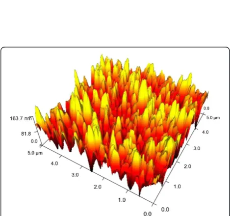
When the two samples were taken out simultaneously from the two beakers, only sample B in the HCCT-MS showed clear hydrophobicity. The mixing process accelerates the whole chemical reaction; nanospike structures are clustered together at the point. In Figure 3, the three-dimensional (3D) topological AFM image (5×5μm2) can reasonably support the above hypothesis. The nanoscale structures together with the few micro-scale features decorating the spikes result in a pro-nounced increase of the overall roughness. The increase of local surface roughness is beneficial for the enhance-ment of surface hydrophobicity. It is assumed that the surface of sample B prepared with this procedure pos-sesses the hydrophobic self-cleaning function due to the second length scale morphology. It is well known that a hydrophobic surface generally refers to a surface with a water contact angle larger than 90°. When a surface has a water contact angle larger than 150°, it is called a superhydrophobic surface.
with a water contact angle of 128° shows a hydrophobic self-cleaning function. In this paper, the silicon wafer has been modified with metal-assisted wet etching. After modification, the water contact angle on the surface of black silicon clustered by nanospike and few microspike structures is adequate to achieve self-cleaning. Accor-ding to the experimental measurement, the mean static contact angle of sample B is approximately 118°, while that of sample A is approximately 82°. The textured sili-con (sample B) with a dualistic structure can imitate Compositae petal leaves ideally.
[image:3.595.310.539.90.441.2]The water contact angles in such cases may be interpreted by describing the Cassie-Baxter wetting state, where liquid drops do not completely penetrate the nanostructures and air pockets are trapped inside the spikes underneath the liquid drop [22-24]. A relationship that describes the contact angle on the textured surface is expressed by the equation cos θCB= f cosθ +f −1, where θCB is the liquid–solid contact angle on the tex-tured surface, θ is the static contact angle on the flat
[image:3.595.58.284.91.419.2]Figure 1Top view of the black silicon produced by metal -assisted chemical wet etching. (a)Sample A in the digital constant temperature water bath.(b)Sample B in the heat collection-constant temperature type magnetic stirrer.
Figure 2Cross section of the black silicon produced by metal -assisted chemical wet etching. (a)Sample A in the digital constant temperature water bath.(b)Sample B in the heat collection-constant temperature type magnetic stirrer.
[image:3.595.304.539.494.714.2]surface, and fis the fraction of the liquid–solid contact area.
Therefore, depending on the value of the f factor, the surface can be either hydrophilic or hydrophobic. Accor-ding to the above equation, the smaller the value off, the higher the increase of the contact angle. So it is essential to make a smaller contact area in order to obtain the higher contact angle. For example, the surface hydropho-bicity can be improved in the preparation of a nanostruc-tured silicon section. The result is consistent with the reports that black silicon was obtained by a photochemical procedure based on anisotropic etching [25].
[image:4.595.57.292.339.675.2]The total optical reflectance spectra of A, B, and un-treated crystalline silicon(C-Si) samples were measured for normal incident covering the spectral regions above and below the bandgap of silicon with a spectrophotom-eter and an integrating sphere detector. As shown in Figure 4a, the reflectance spectrum of the untreated sample (blue dashed line) shows the typical high reflect-ivity as expected, while the reflectance of samples A and
B was drastically suppressed over the spectrum from the UV to the near IR. It is worthwhile to note that the re-flectivity of sample B (red line) is 10% lower than that of sample A (black line). The reflectivity of sample B also increases evidently (23%) beginning from the wavelength of approximately 1,216 nm.
[image:4.595.303.538.485.688.2]The absorption curves of the textured samples in Figure 4b, calculated by the formula A=1 −R −T, also show a stronger absorption than the untreated sample over a broad spectral range. Obviously, the absorption of sample B is strongest in the range of 250 to approxi-mately 1,100 nm. Over the UV–vis spectrum, the ab-sorption of sample B is above 90%, even up to 98%. It is noteworthy that the decrease of reflectance below the bandgap is not accompanied by the increase of absorp-tion, instead of the increased transmittance (as shown in the inset). Both textured and untreated silicon are trans-parent above the wavelength of 1,100nm. It is more im-portant that the total reflectance and absorption of sample B at the wavelength of approximately 1,100 nm are approximately 8.649% and 54.32%, respectively, and the results compared to those of sample A are higher. By the same token, the appearance of random micro-scale spikes can enhance optical absorption inside the material. This behavior can be reasonably explained by multiple scattering effects with second length scale arrays. As shown in Figure 5, the length of spikes in Figure 5b is longer than that in Figure 5a, so the fre-quencies of reflectance in Figure 5b are more. So the more frequencies of reflectance are, more light can be trapped and higher absorption is obtained.
Figure 4Total reflectance and absorption spectra. (a)Total reflectance spectra and(b)total absorption spectra for the A, B, and untreated C-Si samples with wavelength ranging between UV and NIR. The inset shows total transmittance spectra for both treated and untreated samples.
Incident light
a
Incident light
b
Figure 5Optical path of incident light on the black silicon spike structures. (a)Sample A in the digital constant temperature water bath.(b)Sample B in the heat collection-constant
Once black silicon materials are used on solar cells or photovoltaic detectors, dust particles accumulating on the device architectures will seriously imprison sunlight and eventually lead to the reduction of device efficiency and device life. Devices with self-cleaning function can easily avoid the abovementioned problem. It is import-ant that we use simple chemical etching to achieve the self-cleaning function of black silicon surface. It paves the way for our further study on the morphology and topology of textured silicon by chemical etching.
Conclusions
In conclusion, we have demonstrated the self-cleaning function of black silicon surface which was textured by metal-assisted chemical wet etching. SEM and AFM im-ages confirmed that the black silicon surface textured in the HCCT-MS had both micro- and nanoscale struc-tures. The static contact angle of approximately 118° is adequate to make the surface hydrophobic with a self-cleaning performance. The reflectance of sample B is suppressed due to the unique geometry, which is effect-ive for the enhancement of absorption. How to make better use of the feature in a specific environment still requires further study. The novel construction of a hydrophobic surface on black silicon wafer may be ap-plicable to various applications.
Competing interests
The authors declare that they have no competing interests.
Authors’contributions
TZ and PZ designed and carried out the experiments. TZ, PZ, SL, and ZW participated in the work to analyze the data and prepared the manuscript initially. SL, WL, ZW, and YJ gave equipment support. All authors read and approved the final manuscript.
Acknowledgements
This work was partially supported by the National Science Foundation of China via grant no. 61204098. The authors would like to thank the State Key Laboratory of Electronic Thin Films and Integrated Devices in China for the help and equipment support.
Received: 18 June 2013 Accepted: 5 August 2013 Published: 13 August 2013
References
1. Myers RA, Farrell R, Karger AM, Carey JE, Mazur E:Enhancing near-infrared avalanche photodiode performance by femtosecond laser
microstructuring.Appl Optics2006,45:8825.
2. Kabashin AV, Delaporte P, Pereira A, Grojo D, Torres R, Sarnet T, Sentis M:
Nanofabrication with pulsed lasers.Nanoscale Res Lett2010,454:5. 3. Li X, Bohn PW:Metal-assisted chemical etching in HF/H2O2produces
porous silicon.Appl Phys Lett2000,77:2572.
4. Shiu S-C, Lin S-B, Lin C-F:Reducing Si reflectance by improving density and uniformity of Si nanowires fabricated by metal-assisted etching.
Nanomaterials2010,160:4236.
5. Jiang J, Li S, Jiang Y, Wu Z, Xiao Z, Su Y:Enhanced ultraviolet to near-infrared absorption by two-tier structured silicon formed by simple chemical etching.Philos Mag2012,92:4291.
6. Kong D, Junghwa O, Jeon S, Kim B, Cho C, Lee J:Fabrication of black silicon by using RIE texturing process as metal mesh.In17th Opto-Electronics and Communications Conference (OECC): July 2–6 2012; Busan.New York: IEEE; 2012:697–698.
7. Sainiemi L, Jokinen V, Shah A, Shpak M, Aura S, Suvanto P, Franssila S:
Non-reflecting silicon and polymer surfaces by plasma etching and replication.Adv Mater2011,23:122.
8. John GC, Singh VA:Porous silicon: theoretical studies.Physics Reports1995,
263:93.
9. Branz HM, Yost VE, Ward S, Jones KM, To B:Nanostructured black silicon and the optical reflectance of graded-density surfaces.Appl Phys Lett 2009,94:231121.
10. Zhu J, Hsu C-M, Zongfu Y, Fan S, Cui Y:Nanodome solar cells with efficient light management and self-cleaning.Nano Lett2010,10(6):1979. 11. Han JT, Lee DH, Ryu CY, Cho K:Fabrication of superhydrophobic from a
supramolecular organosilane with quadruple hydrogen bonding.
J Am Chem Soc2004,126(15):4796–4797.
12. Lee SE, Lee D, Lee P, Ko SH, Lee SS, Hong SU:Flexible superhydrophobic polymeric surfaces with micro-/nanohybrid structures using black silicon.
Macromol Mater Eng2012,298:311.
13. Nosonovsky M, Bhushan B:Roughness optimization for biomimetic superhydrophobic surfaces.Microsyst Technol2005,11:535. 14. Ling XY, Phang IY, Vancso GJ, Huskens J, Reinhoudt DN:Stable and
transparent superhydrophobic nanoparticle films.Langmuir2009,
25:3260.
15. Zorba V, Persano L, Pisignano D, Athanassiou A, Stratakis E, Cingolani R, Tzanetakis P, Fotakis C:Making silicon hydrophobic: wettability control by two-lengthscale simultaneous patterning with femtosecond laser irradiation.Nanotechnology2006,17(13):3234.
16. Shirtcliffe NJ, Aqil S, Evans C, McHale G, Newton MI, Perry CC, Roach P:The use of high aspect ratio photoresist (SU-8) for super-hydrophobic pattern prototyping.J Micromech Microeng2004,14(10):1384. 17. Krupenkin TN, Taylor JA, Schneider TM, Yang S:From rolling ball to
complete wetting: the dynamic tuning of liquids on nanostructured surfaces.Langmuir2004,20:3824.
18. Huang Z, Geyer N, Werner P, de Boor J, Gosele U:Metal-assisted chemical etching of silicon: a review.Adv Mater2011,23:285.
19. Chartier C, Bastide S, Levy-Clement C:Metal-assisted chemical etching of silicon in HF-H2O2.Electrochim Acta2008,53:5509.
20. Kolasinski KW:Silicon nanostructures from electroless electrochemical etching.Curr Opin Solid State Mater Sci2005,9(1–2):73–83.
21. Barthlott W, Neinhuis C:Purity of the sacred lotus, or escape from contamination in biological surfaces.Planta1997,202:1.
22. Cassie ABD, Baxter S:Wettability of porous surfaces.Trans Faraday Soc 1944,40:546.
23. Marmur A:Wetting on hydrophobic rough surfaces: to be heterogeneous or not to be?Langmuir2003,19:8343.
24. Dawood MK, Liew TH, Lianto P, Hong MH, Tripathy S, Thong JTL, Choi WK:
Interference lithographically defined and catalytically etched, large-area silicon nanocones from nanowires.Nanotechnology2010,21(20):205305. 25. Dorrer C, Rühe J:Wetting of silicon nanograss: from superhydrophilic to
superhydrophobic surfaces.Adv Mater2008,20:159.
doi:10.1186/1556-276X-8-351
Cite this article as:Zhanget al.:Black silicon with self-cleaning surface prepared by wetting processes.Nanoscale Research Letters20138:351.
Submit your manuscript to a
journal and benefi t from:
7 Convenient online submission
7 Rigorous peer review
7 Immediate publication on acceptance
7 Open access: articles freely available online
7 High visibility within the fi eld
7 Retaining the copyright to your article