N A N O E X P R E S S
Open Access
The interfaces of lanthanum oxide-based
subnanometer EOT gate dielectrics
Hei Wong
1,2*, Jian Zhou
1, Jieqiong Zhang
2, Hao Jin
1, Kuniyuki Kakushima
3and Hiroshi Iwai
3Abstract
When pushing the gate dielectric thickness of metal-oxide-semiconductor (MOS) devices down to the subnanometer scale, the most challenging issue is the interface. The interfacial transition layers between the high-kdielectric/Si and between the high-kdielectric/gate metal become the critical constraints for the smallest achievable film thickness. This work presents a detailed study on the interface bonding structures of the tungsten/lanthanum oxide/silicon (W/La2O3/ Si) MOS structure. We found that both W/La2O3and La2O3/Si are thermally unstable. Thermal annealing can lead to W oxidation and the forming of a complex oxide layer at the W/La2O3interface. For the La2O3/Si interface, thermal annealing leads to a thick low-ksilicate layer. These interface layers do not only cause significant device performance degradation, but also impose a limit on the thinnest equivalent oxide thickness (EOT) to be achievable which may be well above the requirements of our future technology nodes.
Keywords:High-k; Lanthanum oxide; Si/high-kinterface; Metal gate/high-kinterface
Background
In the deca-nanometer complementary metal-oxide-semiconductor (CMOS) devices, the thickness of the gate dielectric film should be scaled down to the subnanometer equivalent oxide thickness (EOT) range in order to have proper control of the channel current under a reasonable gate bias [1-3]. This ultimate dielectric thickness require-ment imposes a number of challenges on both the fabrica-tion process and the device characteristic optimizafabrica-tion. Interface properties and their thermal instabilities turn out to be the major challenging issues. Transition metal (TM)- or rare earth metal (RE)-based high-k dielectrics are extrinsic materials to the substrate silicon; they can react with silicon at some elevated temperatures [4-8], and the chemical reactions at the high-k/silicon interface cause most of the performance degradation issues. Conventional MOS layout for large-scale integration is in the planar structure, and the channel mobility of the transistors is predominately governed by the dielectric/silicon interface. Improvement of the SiO2/Si interface property had been one of the major concerns since the invention of the MOS
transistor regardless of the fact that the SiO2/Si interface is already almost perfect as it is grown thermally in a self-organizing way from the intrinsic material [9-11], whereas the quality of the high-k metal/Si interface was found to be much poor. It was found that there exists a relative low-k transition layer between the TM/RE metal oxide and substrate silicon [12,13]. This low-k layer may be of several angstroms to a nanometer thick and may become the major portion of the subnanometer EOT dielectric film. This transition layer, which cannot be scaled down for thinner high-kfilms, has become the major challenging issue for the subnanometer EOT thin film [1,2]. The metal gate/high-k interface where a low-k transition layer may exist will also affect the resulting EOT; unfortunately, this issue was seldom studied. In this work, we took the tung-sten/lanthanum oxide/Si (W/La2O3/Si) structure as an ex-ample to have a detailed study on the bonding structures together with thermal annealing effects on the W/La2O3 interface and La2O3/Si interface by employing combined angle-resolved X-ray photoelectron spectroscopy (ARXPS) and film thinning with in situ sputtering using an XPS source.
Methods
The tungsten/La2O3gate stack was deposited on the n-type Si (100). A La2O3 film of about 5 nm thick was * Correspondence:[email protected]
1
Department of Electronic Engineering and Information Sciences, Zhejiang University, Hangzhou, China
2
Department of Electronic Engineering, City University of Hong Kong, Tat Chee Avenue, Kowloon, Hong Kong
Full list of author information is available at the end of the article
prepared by electron beam evaporation in an ultra-high vacuum chamber with a pressure of about 10−7 Pa. A tungsten gate electrode of about 3 nm thick was then deposited in situ using magnetron sputtering to avoid any moisture absorption and contamination. Some sam-ples were further thermally annealed at 600°C for 30 min in a rapid thermal annealing furnace. The chemical compositions as well as the bonding structures of the as-prepared W/La2O3/Si stack at different depths were inves-tigated in detail by using a Physical Electronics PHI 5802 spectrometer (Physical Electronics, Inc., Chanhassen, MN, USA) with monochromatic Al Kαradiation with an energy of 1,486.6 eV. To study the bonding structure on both W/ La2O3 and La2O3/Si interfaces, both depth profiling by argon sputtering and angle-resolved techniques were used.
Results and discussion High-k/metal gate interface
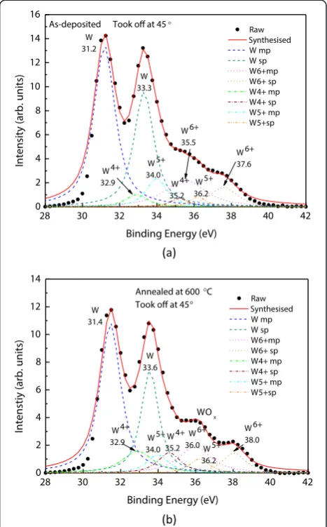
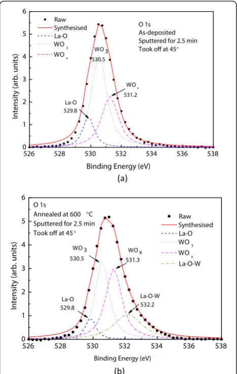
The high-k/metal gate interfacial layer can be either an insulating layer or a conductive layer. For the conven-tional poly-Si gate, a thick insulating silicate layer can be formed. For the La2O3/Al stack, the interfacial layer is aluminum oxide or lanthanum aluminates. These inter-face layers generally have much smaller k values (<15) than the desired high-k gate dielectric. The thickness of this transition layer may range from 0.3 to over 1 nm de-pending on the material and the post high-kdeposition temperature. With this low-k transition layer, subnan-ometer EOT is hard to be achieved. It will be good if the transition layer between metal/high-k, e.g., W/La2O3 stack, is conductive. By using angle-resolved XPS with take-off angle varying from 0° to 90° together with argon sputtering for film thinning, bonding details along the depth direction were obtained in this work. Oxidized tungsten phases were found both on the surface and at the W/La2O3 interface. Figure 1 depicts the W 4f XPS spectra taken from a W/La2O3 stack with a take-off angle of 45°. The elemental W has a doublet with ener-gies at 31.2 and 33.3 eV. By employing Gaussian decom-position technique, several oxidized states were observed for both as-deposited and thermally annealed samples. These results indicate that there exist WOxphases in the transition layer. The W atoms in WOxform are in d2 con-figuration, and that makes the WOxconductive. Thermal annealing at 600°C can enhance the W oxidation at the W/La2O3interface significantly (see Figure 1b). These ob-servations were further confirmed with the O 1s XPS spectra. Figure 2 shows the O 1s XPS for both as-deposited and 600°C annealed samples. Gaussian decom-position of the O 1s peak indicates that the oxygen in the as-deposited film has three main bonding states with ener-gies of 528.9, 530.5, and 531.2 eV corresponding respect-ively to La-O, WO3, and WOx bonding. After thermal annealing at 600°C for 30 min, the WOx phase was
significantly enhanced. The oxygen for interface W oxida-tion should come from the La2O3film. It was proposed that the oxygen in W may diffuse into the La2O3film to fill up the oxygen vacancies there [14]. Oxygen vacancies are the major defect centers in La2O3which result in sev-eral instability issues and enhance the gate leakage current [15-17]. The present result indicates that a reverse process may have been taken place in the present samples. That means a high-temperature process may lead to the out-diffusion of oxygen to the W/La2O3interface, and that in-creases oxygen vacancies in the La2O3film. In addition, La-O-W bonding with a peak energy of 532.2 eV was found. For the case of WOxphase enhancement, it should not affect the EOT as it can be considered as part of the metal electrode; on the other hand, the effects of La-O-W bonding have never been explored, and it should have some impact in making the effective EOT thicker.
28 30 32 34 36 38 40 42 0 2 4 6 8 10 12 14 16 W 5+ 36.2 W 4+ 35.2 W 5+ 34.0 W 4+ 32.9 W 6+ 37.6 W 6+ 35.5 W 33.3 W 31.2
As-deposited Took off at 45
Intensity (arb. units)
Binding Energy (eV)
Raw Synthesised W mp W sp W6+mp W6+ sp W4+ mp W4+ sp W5+ mp W5+sp (a)
28 30 32 34 36 38 40 42 0 2 4 6 8 10 12 14 W 5+ 36.2 W 6+ 38.0 W 6+ 36.0 W 4+ 35.2 W 5+ 34.0 W 33.6 W 4+ 32.9 W 31.4
Annealed at 600 C Took off at 45
Intenstiy (arb. units)
Binding Energy (eV)
[image:2.595.305.539.90.466.2]Raw Synthesised W mp W sp W6+mp W6+ sp W4+ mp W4+ sp W5+ mp W5+sp WOx (b)
Figure 1W 4f XPS spectra with Gaussian decomposition.This figure shows various oxidized states of tungsten near the W/La2O3
Silicon/high-kinterface
High-kcan react, especially in the presence of a silicon oxide layer, with the silicon substrate, and the electronic bonding structure at the La2O3/Si interface should be much more complicated than the SiO2/Si case. It was known that the interface bonding may lead to either an insulating layer (silicate bonding) or conductive layer (silicide bonding) [1,2]. Most of the high-ksilicides are conductive. The interfacial silicide layer will not affect the EOT but the interface metal-Si bonding in the inter-face trap precursors and results in the channel mobility degradation and other instabilities [1,15,16]. Most of the high-k materials including hafnium oxide and lan-thanum oxide are only marginally stable against the for-mation of silicates. The device properties can be improved with the interfacial silicate layer [1]. However, this layer has much smaller k values and becomes the
lower bound of the thinnest EOT, and needs to be mini-mized for the subnanometer EOT dielectric. Figure 3 shows the La 3d XPS spectra at different depths. The dif-ferent depths were obtained by argon sputtering for 2.5 to 8 min, and all the XPS analyses were made at a take-off angle of 45°. This treatment should be able to minimize the artifacts due to ion knock-on effects. The bulk La 3d3/2 XPS spectra shows a main peak energy of 851.9 eV and a satellite peak energy of 855.6 eV [1]. As sputtered closer to the substrate, the main peak of La 3d3/2shifts to an even higher energy side of 852.6 eV, and the intensity of the sat-ellite peak becomes weaker, indicating that more silicate with La-O-Si bonding formed at the interface [13]. This trend is more obvious for the sample with thermal anneal-ing (see Figure 3b). Figure 3c depicts the O 1s bondanneal-ing states near the La2O3/Si interface for the 600°C annealed sample. With Gaussian decomposition, three oxygen bond-ing states, i.e., La-O, La-O-Si, and Si-O, were found. It indi-cates that the thermal annealing does not only lead to the formation of the interfacial silicate layer, but also results in the Si substrate oxidation. Figure 4 depicts the cross-sectional view of the W/La2O3/Si structure for the sample annealed at 600°C for 30 min; a thick silicate layer of about 2 nm was found at the interface. This thickness of layer is quite substantial as the original film thickness is 5 nm only. With capacitance-voltage measurements, thekvalue of this layer is estimated to be in the range of 8 to 13. Thus, from the EOT point of view, this layer contributes over 0.5 nm of the total thickness. In addition, the interface roughness was significantly increased which led to further channel mobility degradation. Hence, although some of the device properties may be improved by forming the interfacial sili-cate layer and SiO2 layer, the silicate or SiO2 layer has much smallerkvalue and becomes the lower bound of the thinnest EOT. It needs to be minimized for the subnan-ometer EOT dielectric.
It is further noted that the TEM picture also shows a rough interface between La2O3and W. The rough inter-face should be due to the oxidation of tungsten and the reaction between La2O3 and tungsten at the interface. Although in real device applications, the W/La2O3 will not undergo such high-temperature annealing, the inter-face reaction should still exist in a certain extent as a similar phenomenon was also found in the sample which had undergone post-metallization annealing only [14].
Thermal budget and process sequences
As mentioned, the interface between the high-k/Si and thermal stability have become the most challenging issues for next-generation subnanometer EOT gate dielectrics. Unlike silicon oxide or silicon nitride, high-kmetal oxides are less thermally stable and are easier to be crystallized [1,18]. A low-temperature treatment such as post-metallization annealing (PMA) of about 350°C may still
526 528 530 532 534 536 538
0 1 2 3 4 5 6
WOx 531.2 La-O
529.8 WO 3 530.5
O 1s As-deposited Sputtered for 2.5 min Took off at 45
Intensity (arb. units)
Binding Energy (eV)
Raw Synthesised
La-O WO3 WOx
(a)
526 528 530 532 534 536 538 0
1 2 3 4 5 6
La-O-W 532.2 La-O
529.8
WO x 531.3 WO 3
530.5 O 1s
Annealed at 600 C Sputtered for 2.5 min Took off at 45
Raw Synthesised
La-O WO3 WOx La-O-W
Intensity (arb. units)
Binding Energy (eV)
[image:3.595.57.291.89.458.2](b)
Figure 2O 1s spectra taken near the W/La2O3interface. (a)
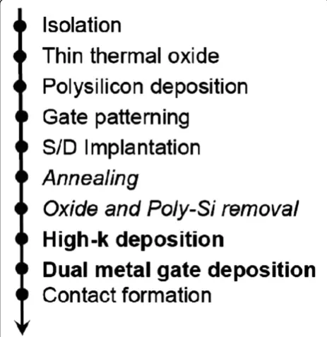
lead to local crystallization of the dielectric [1,18]. Ther-mal processing above 500°C will result in the interface oxi-dation and the formation of a interfacial silicate layer. At even higher temperatures, serious crystallization, partial decomposition of metal-oxygen bonds, and phase separ-ation of silicate will occur [1,2]. Thus, the process se-quence of a high-k-based process has to be adjusted so as to avoid the as-deposited high-kmaterial from being ex-posed at a high-temperature ambient. In addition, to avoid the knock-on of metal atoms into the substrate, the high-k film should not be deposited before the ion implantation unless a very thick protection layer is introduced. Several processes, namely, gate-first, gate-last, source/drain first, and combined methods, were proposed [1]. The gate-first process is similar to the conventional one. It requires both
Figure 3XPS results showing the existence of interfacial silicate layer at the La2O3/Si interface. (a)La 3d spectra of the
as-deposited sample.(b)La 3d spectra of the thermally annealed sample.(c)O 1s spectrum taken from the La2O3/Si interface region
for the annealed sample.
Si Substrate W
[image:4.595.306.539.90.198.2]La Silicates k = ~8-14 EOT > 0.5 nm Bulk La2O3 k = 23
Figure 4A TEM picture showing the cross-sectional view of the W/La2O3/Si stack.A silicate layer of about 2 nm thick was found.
[image:4.595.305.537.446.685.2]the high-kand the gate electrode material to be stable at the annealing temperature. In addition, the source/drain doping may produce damages to the gate dielectric also. High-temperature post-implant annealing will also result in the growth of the interfacial layer at the high-k/Si inter-face. The high-temperature process also led to the non-uniformity of the film thickness. Hence, the gate-first process cannot be used with the subnanometer EOT gate dielectric in the deca-nanometer CMOS technol-ogy. In the gate-last process, the high-k dielectric was deposited and then an intermediate poly-Si layer was deposited and patterned. After the source/drain im-plantation and salicidation process, the poly-Si gate was replaced with the metal gate. This process avoids the possible knock-on of the high-kmetal into the substrate and minimizes the number of high-temperature cycles on the gate material. However, this process still causes the high-k layer to be exposed to high temperatures. This drawback was resolved with the‘source/drain first’ process [19]. Figure 5 shows a modified source/drain first process sequence for high-kintegration. This process reduces the interfacial low-klayer growth and seems to be a viable option for preparing the ultimate EOT dielectric film although there are some disadvantages associated with this process sequence re-shuttling.
Conclusions
In future technology nodes, the gate dielectric thickness of the CMOS devices will be scaled down to the subnan-ometer range. Lanthanum-based dielectric films have been considered to be suitable candidates for this application. This work presented a detailed study on the interface bonding structures of the W/La2O3/Si stack. We found that thermal annealing can lead to W oxidation and for-mation of a complex oxide layer at the W/La2O3interface. For the La2O3/Si interface, thermal annealing leads to a thick low-k silicate layer. These interface layers will be-come the critical constraint for the smallest achievable EOT, and they would also cause a number of instability is-sues and induce device performance degradation. These issues can be minimized by lowering the thermal budgets and re-shuttling the process sequences.
Competing interests
The authors declare that they have no competing interests.
Authors’contributions
HW generated the research idea, analyzed the data, and wrote the paper. JZ and HJ were involved in some of the sample preparation and TEM experiments. JeZ performed the XPS analysis. KK and HI provided the samples. HW has given final approval of the version to be published. All authors read and approved the final manuscript.
Acknowledgements
This work is supported by the National Natural Science Foundation of China under grant no. 61376111.
Author details 1
Department of Electronic Engineering and Information Sciences, Zhejiang University, Hangzhou, China.2Department of Electronic Engineering, City
University of Hong Kong, Tat Chee Avenue, Kowloon, Hong Kong.3Frontier Research Center, Tokyo Institute of Technology, Yokohama 226-8502, Japan.
Received: 6 July 2014 Accepted: 15 August 2014 Published: 5 September 2014
References
1. Wong H, Zhang J:Challenges of next generation ultrathin gate dielectrics.InProc IEEE Int Symp Next Generation Electronics; Taoyuan.
Piscataway: IEEE Press; 2014.
2. Wong H:Nano-CMOS Gate Dielectric Engineering.Boca Raton: CRC Press; 2012. 3. Wong H, Iwai H:On the scaling issues and high-k replacement of
ultrathin gate dielectrics for nanoscale MOS transistors.Microelectron Engineer2006,83:1867–1904.
4. Lichtenwalner DJ, Jur JS, Kingon AI, Agustin MP, Yang Y, Stemmer S, Goncharova LV, Gustafsson T, Garfunkel E:Lanthanum silicate gate dielectric stacks with subnanometer equivalent oxide thickness utilizing an interfacial silica consumption reaction.J Appl Phys2005,98:024314. 5. Yamada H, Shimizu T, Suzuki E:Interface reaction of a silicon substrate and lanthanum oxide films deposited by metalorganic chemical vapor deposition.Jpn J App Phys2002,41:L368–370.
6. Wong H, Ng KL, Zhan N, Poon MC, Kok CW:Interface bonding structure of hafnium oxide prepared by direct sputtering of hafnium in oxygen.J Vac Sci Technol B2004,22:1094–1100.
7. Lucovsky G:Bond strain and defects at Si-SiO2and dielectric interfaces in
high-k gate stacks.InFrontiers in Electronics.Edited by Iwai H, Nishi Y, Shur MS, Wong H. Singapore: World Scientific; 2006:241–262.
8. Lucovsky G:Electronic structure of transition metal/rare earth alternative high-k gate dielectrics: interfacial band alignments and intrinsic defects.
Microeletron Reliab2003,43:1417–1426.
9. Lucovsky G, Phillips JC:Microscopic bonding macroscopic strain relaxations at Si-SiO2interfaces.Appl Phys A2004,78:453–459. 10. Fitch JT, Bjorkman CH, Lucovsky G, Pollak FH, Yim X:Intrinsic stress and
stress gradients at the SiO2/Si interface in structures prepared by
thermal oxidation of Si and subjected to rapid thermal annealing.J Vac Sci Technol B1989,7:775–781.
11. Lucovsky G, Yang H, Niimi H, Keister JW, Rowe JE, Thorpe MF, Phillips JC:
Intrinsic limitations on device performance and reliability from bond-constraint induced transition regions at interfaces of stacked dielectrics.J Vac Sci Technol B2000,18:1742–1748.
12. Wong H, Iwai H:Modeling and characterization of direct tunneling current in dual-layer ultrathin gate dielectric films.J Vac Sci Technol B
2006,24:1785–1793.
13. Wong H, Iwai H, Kakushima K, Yang BL, Chu PK:XPS study of the bonding properties of lanthanum oxide/silicon interface with a trace amount of nitrogen incorporation.J Electrochem Soc2010,157:G49–G52. 14. Kawanago T:A study on high-k/metal gate stack MOSFETs with rare earth
oxides.InPh.D. Dissertation.Japan: Tokyo Institute of Technology; 2011. 15. Wong H, Sen B, Yang BL, Huang AP, Chu PK:Effects and mechanisms of
nitrogen incorporation in hafnium oxide by plasma immersion implantation.J Vac Sci Technol B2007,25:1853–1858.
16. Wong H, Yang BL, Kakushima K, Ahmet P, Iwai H:Effects of aluminum doping on lanthanum oxide gate dielectric films.Vacuum2012,86:929–932. 17. Sen B, Wong H, Molina J, Iwai H, Ng JA, Kakushima K, Sarkar CK:Trapping
characteristics of lanthanum oxide gate dielectric film explored from temperature dependent current-voltage and capacitance-voltage measurements.Solid State Electron2007,51:475–480.
18. Perevalov TV, Gritsenko VA, Erenburg SB, Badalyan AM, Wong H, Kim CW:
Atomic and electronic structure of amorphous and crystalline hafnium oxide: x-ray photoelectron spectroscopy and density functional calculations.J Appl Phys2007,101:053704.
19. Sakamoto K, Huda M, Ishii K:Self-aligned planar double-gate field-effect transistors fabricated by a source/drain first process.Jpn J Appl Phys2005,44:L147.
doi:10.1186/1556-276X-9-472