N A N O E X P R E S S
Open Access
Phase-Selective Synthesis of CIGS
Nanoparticles with Metastable Phases
Through Tuning Solvent Composition
Xiaokun Zhang
1, Shuai Liu
1, Fang Wu
1, Xiaoli Peng
1, Baoguo Yang
2and Yong Xiang
1*Abstract
I-III-VI2compounds have shown great interests in the application of functional semiconductors. Among them, Cu(In,Ga) S2has been a promising candidate due to its excellent optoelectronic properties. Although the polymorphs of Cu(In,Ga)S2 have been attracted extensive attentions, the efforts to developing the methodologies for phase-controlled synthesis of them are rare. In this paper, we reported a phase-selective synthesis of CIGS nanoparticles with metastable phases via simply changing the composition of solvents. For the wet chemistry synthesis, the microstructure of the initial nuclei is decisive to the crystal structure of final products. In the formation of Cu(In,Ga)S2, the solvent environment is the key factor, which could affect the coordination of monomers and influence the thermodynamic conditions of Cu-S nucleation. Moreover, wurtzite and zincblende Cu(In,Ga)S2 nanoparticles are selectively prepared by choosing pure en or its mixture with deionized water as reaction solvent. The as-synthesized wurtzite Cu(In,Ga)S2possess a band gap of 1.6 eV and a carrier mobility of 4.85 cm
2 /Vs, which indicates its potential to construct a heterojunction with hexagonal-structured CdS for solar cells.
Keywords:CIGS, Nanoparticles, Metastable, Wurtzite, Zincblende, Phase-selective
Introduction
I-III-VI2 compound semiconductors hold great promises
for the applications of photoelectric devices, due to their advantageous optical and electrical properties [1–5]. Espe-cially, the thin-film solar cells based on Cu(In,Ga)Se2 (CIGSe) have achieved the energy conversion efficiency higher than 22% [6]. However, compared with silicon-based photovoltaic technologies, the cost of solar cells based on compound semiconductors still need to be reduced signifi-cantly [7]. Recently, CuInS2(CIS) and Cu(In,Ga)S2(CIGS), in which selenium (Se) is replaced by the less toxic and cheaper sulfur (S), garnered great interests as appealing al-ternatives to CIGSe [8–10]. Besides the choice of materials, it is generally believed that the non-vacuum process based on the suspension of nanoparticles (NPs) is also promising in the reduction of the cost of CIGS-based solar cells [7,
11]. Therefore, CIGS NPs play a vital role in the develop-ment of low-cost thin-film solar cells [12–14].
In the past two decades, many efforts have been made to synthesize the chalcogenide NPs with desired proper-ties for photovoltaic application [15–21]. Phase control is one of the most important point for the synthesis of chal-cogenide NPs because their optoelectronic properties
de-pend on the crystal structure [22–26]. According to
literatures [27–29], CIGS may have three polymorphs: a thermodynamically stable phase with tetragonal chalco-pyrite (CH) structure and two metastable phases with cubic zincblende (ZB) structure and hexagonal wurtzite (WZ) structure, respectively. Previous studies mainly fo-cused on the CH-structured CIS and CIGS [18, 30, 31]. Metastable ZB- and WZ-structured CIS NPs prepared via hot-injection approach were firstly reported by Pan et al. in 2008 [32]. After that, CIS NPs with metastable phase were also obtained by solvothermal synthesis [33,34] and thermal decomposition of precursors [35, 36]. However, to our best knowledge, all these previous reports on the synthesis of metastable phase CIS or CIGS invlove indu-cible additives [37, 38], expensive ligands [32, 39], or
* Correspondence:[email protected]
1School of Materials and Energy, University of Electronic Science and
Technology of China, 2006 Xiyuan Avenue, West High-Tech Zone, Chengdu 611731, Sichuan, China
Full list of author information is available at the end of the article
complex precursors [34–36]; a low-cost and facile synthe-sis of CIGS NPs still remains challenging.
The formation of NPs generally includes two steps, namely the nucleation step and the crystalline growth step [40,41]. Previous studies [26,42,43] consistently in-dicate that CIGS NPs were formed in two steps: (1) the for-mation of Cu-S crystal nuclei via the rapid reaction between Cu+and S2−; and (2) the incorporation of indium and gallium into the Cu-S crystal nuclei through the diffu-sion and/or cation exchanging. In addition, the crystal structure of final CIGS NPs may mainly depend on the structure of Cu-S nuclei [25, 35, 44]. Herein, we report a one-pot solvothermal synthesis of CIGS NPs with metasta-ble phases, without the requirements of additives, expensive ligands, or preparation of complex precursors. By simply changing the composition of solvents for solvothermal re-action, the thermodynamic environment of Cu-S nucleation can be tuned, in turn ZB- or WZ-structured CIGS NPs can be selectively obtained. In addition to the discussion of the mechanism of phase-selective synthesis, the electrical and optical properties of the products with different crystal structures are also compared in this study.
Experimental Methods Materials
CuCl2·2H2O (99.9%), sulfur powder (99.9%), anhydrous ethylenediamine (en, 99%), and anhydrous ethanol (99.7%) were purchased from Chengdu Kelong Chemical
Co., Ltd. InCl3 (99.9%) was purchased from Aladdin.
Ga(acac)3 (99.99%) was purchased from Sigma-Aldrich.
All the chemicals were used as received.
Solvothermal Synthesis of CIGS NPs
For the synthesis of WZ-structured CIGS NPs, a metal
precursor solution was prepared by dissolving
CuCl2·2H2O (0.164 g, 0.96 mmol), InCl3 (0.192 g,
0.868 mmol), and Ga(acac)3 (0.068 g, 0.186 mmol) in
5 ml ethylenediamine. Sulfur powder (0.0826 g,
2.58 mmol) was dispersed in 5 ml ethylenediamine through an ultrasonic treatment at 60 °C for 15 min. The metal precursor solution was mixed with the disper-sion of sulfur in a 20-ml Teflon-lined autoclave. About 6 ml ethylenediamine was then added to make the vol-ume of the reaction solution is 80% of that of the Teflon-lined autoclave. The autoclave was sealed and treated with sonication at 60 °C for 15 min. Thereafter, the autoclave was put into an oven. The temperature in the oven was raised from room temperature to 200 °C and maintained for 24 h, and then cooled down to room temperature naturally. The precipitate was separated by centrifugation, washed with a mixed solvent of ethanol and deionized water for five times, and dried in vacuum at 60 °C for 4 h.
For the synthesis of ZB-structured CIGS NPs, the metal precursor solution was prepared by dissolving metal salts in 5 ml deionized water. Other procedures and synthetic conditions were unchanged.
Characterization
The phase of the as-synthesized NPs was identified by X-ray diffraction (XRD) on a Bruker D8 Advance
dif-fractometer equipped with monochromatized Cu-Kα (λ
= 1.5418 Å) radiation. The diffraction data was collected with an angle increment of 0.02° at a scan rate of 0.1 s/ step. Scanning electron microscopy (SEM) images were
obtained using a ZEISS EVO@ LS15 SEM operated
under 15 kV. The ZEISS EVO@ LS15 SEM is equipped
with a Bruker Nano GmbH XFlash Detector 5010, which was used to estimate the stoichiometric proportion by energy dispersive X-ray spectroscopy (EDS). The optical properties of the as-prepared products were characterized by an Agilent Cary5000 UV-Vis-IR spectrophotometer. The electrical properties were calculated based on Hall ef-fect measurements using Swin Hall 8800 system. The as-synthesized CIGS NPs were deposited on glass sub-strates via spray coating, and electrical contacts were formed by silver paste for Hall effect measurements. The species in precursor solutions were studied by UV-Vis-IR spectrophotometer (Agilent Cary5000) and Raman spec-trophotometer (Renishaw Invia).
Results and Discussion
For the synthesis of CIGS NPs, sulfur (S) dispersed in ethylenediamine (en) was mixed with the metal salts that dissolved in en or deionized water. And then, the mix-tures with different solvent compositions were ultrasonic treated at 60 °C for 15 min, followed by reacted at 200 ° C for 24 h under the solvothermal condition. en with a dual amine group and a short carbon chain was used to stabilize the metastable phase CIGS. As shown in Fig.1, the XRD peaks of the as-synthesized NPs are well identi-cal with the reported wurtzite CIS pattern [32–34], indi-cating that crystal of the fabricated NPs derived from pure en solvent is a hexagonal wurtzite structure. Mean-while, for NPs prepared in the mixing solvent of en and deionized water, the XRD pattern is well consistent with that of the ZB-structured CIS [32, 34, 39]. Thus, the phase-selective synthesis of CIGS NPs with metastable phase can be achieved by simply altering the compos-ition of reaction solvent.
investigate the impact of solvent composition on the sta-tus of sulfur, the Raman spectra of en solvent, en/water mixture, the solution of S in en, and the solution of S in
en/water mixture were collected. As shown in Fig. 2, a
split peak at 811 cm−1can be observed in the spectrum of the solution of S in en, while it is absent from the other three counterparts. This split peak may indicate the status of sulfur precursor in the pure en is different from that in the en/water mixture. It seems that the introduction of H2O would weaken the interaction between S and amino group (see the blue line in Fig.2). Furthermore, en can act as a strong chelating agent for metal ions due to its feature of dual amine group. The amine coordination to Cu2+ dif-fers in the pure en and the mixture of en and deionized water, which is indicated by the fact that the color of the en solution of CuCl2is dark green while that of aqueous solution of CuCl2is blue. Based on the stability constant and dissociation equilibrium of complexes, the molar
con-centration of free Cu2+ in the pure en and water are
evaluated to be 3.12 × 10⁻²²M and 0.192 M, respectively (see the calculation details in Additional file 1). Raman spectra of the solutions of CuCl2in pure en and the mix-ture of en and water seem to be similar (Additional file1: Figure S1). This should ascribe to the vibrations of Cu– NH2chelating bond exists in both two solutions. Figure3
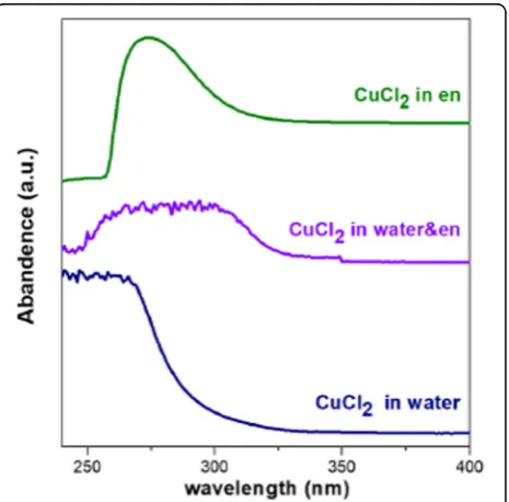
shows absorption spectra of the solutions of CuCl2in pure en, water, and their mixture. The broad absorption at 250–350 nm of CuCl2in the mixture solvent implies that
the coordinating status of Cu2+ may be a balanced
com-bination of that in pure en and water. Take the evaluated concentration of free Cu2+ in consideration, it is reason-able to propose that there are a larger number of free monomers ready to react with S precursor at a relative low temperature in the en/H2O mixture than in that pure en. For the reaction in the mixture solvent, the free Cu2+ Fig. 1XRD patterns of CIGS NPs synthesized in pure en solvent (a) and en/water mixture solvent (b)
Fig. 2Raman spectra of pure en (purple line), the mixture of en and deionized water (blue line), the solutions of the S precursor in pure en (green line), and the solutions of the S precursor in the mixture of en and deionized water (red line)
[image:3.595.58.539.88.211.2] [image:3.595.307.540.465.694.2] [image:3.595.58.290.495.682.2]may react with elemental S to from Cu-S nuclei at moder-ate temperature. Meanwhile, the nucleation of Cu-S in
pure en may happen at elevated temperature between Cu2
+
and S2n−, since high temperature facilitates the dissoci-ation of Cu[en]2+complex and the reduction of elemental S by pure en [45]. Thus, the different solvent environ-ments result in the different thermodynamic conditions and reacting species for Cu-S nucleation, in turn leading to different microstructures of Cu-S clusters. After incorp-oration of In and Ga into the Cu-S clusters, CIGS NPs with different crystal structure can be obtained from pure en and its mixture with water, respectively. According to the mechanism presented here, the minor peak at ~ 32° in
Fig. 1a, which may be indexed to ZB-structured CIGS,
should attribute to the trace water existing in en solvents.
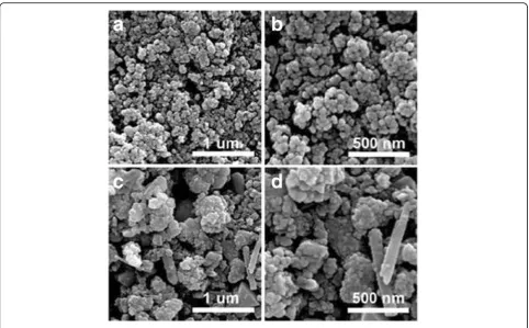
The composition of reaction solvents can also affect the morphologies of as-prepared CIGS NPs. The WZ-struc-tured CIGS NPs, which is derived from pure en, exhibit a uniform particulate morphology with a diameter of 50 nm and are fairly monodispersed (Fig. 4a, b). However, the monodispersity of ZB-structured CIGS NPs is poor, and its morphology is much more complex. The nanoscale pellets, flakes, and rods can be observed in Fig.4c, d. Such
a morphology difference is consistent with the
[image:4.595.57.540.86.385.2]solvent-dependent reaction mechanism proposed above. For the synthesis of WZ-structured CIGS NPs in pure en, the nucleation is difficult at a low temperature because of the chelating bond between en and Cu2+. At an elevated temperature, free metallic monomers are provided by the dissociation of complex compounds, and S precursor is in a reactive and soluble form of S2n−. High concentration of monomers and homogeneous reaction environment trend to generate numerous Cu-S nuclei. Thus, most of mono-mers are consumed by the nucleation, and the growth of the clusters is limited. This process is beneficial to the uni-form and fine morphology of the resultant NPs. Meanwhile, the nucleation of Cu-S is possible to happen at a low temperature during the synthesis of ZB-structured CIGS, because considerable free Cu2+exist in the mixture of en and water at a room temperature, and they may react with solid elemental S. The supplementary reactive monomers Fig. 4Representative SEM images of WZ-structured (a,b,c) and ZB-structured (c,b,d) CIGS NPs
Table 1Composition of WZ- and ZB-structured CIGS NPs (calculated by the measured atomic ratios derived from EDS, the listed ratios are the average of 6 measured values from three individual samples)
Sample Cu:In:Ga:S Cu:(In+Ga) [0.5Cu+1.5(In+Ga)]:S
WZ-CIGS 1:0.86:0.30:2.16 1:1.16 1:0.96
[image:4.595.56.292.691.732.2]provided at high temperature would trend to facilitate the growth of clusters but not to generate new nuclei, through reaction at the solution-solid interfaces [40,41]. In addition, en molecular cannot provide a strong spatial confinement effect to the clusters during its growth, because the seg-ments of en molecular are short. Thus, ZB-structured CIGS NPs show various shapes, such as pellets, flakes, and rods. Slight clustering of the NPs observed in SEM images may be caused by the solvent evaporation during testing sample preparation.
The composition of the as-prepared CIGS NPs was de-termined using EDS, and the results were summarized in
Table 1. The element composition in WZ- and
ZB-structured CIGS NPs is approximately consistent with the stoichiometric chemical composition. However, both of them show a slight sulfur-poor feature, i.e., [0.5Cu
+1.5(In+Ga)]:S = 1:0.96 and 1:0.91 for WZ- and
ZB-structured GIGS respectively, even though ~ 35% ex-cess sulfur was applied in the starting materials. This devi-ation from stoichiometry can be remedied by a heat treatment in sulfur atmosphere during the fabrication of CIGS absorber layers via NPs-based non-vacuum ap-proaches. It can be seen that WZ-structured CIGS NPs possess a copper-poor characteristic (Cu:(In+Ga) = 1:1.16) which is desirable for photovoltaic applications [46], while the ZB-structured one is slight copper-rich (Cu:(In+Ga) = 1:0.96). This indicates that the solvent composition may have a kinetic influence on the incorporation of In and Ga into Cu-S clusters. The pure en environment might in-duced a favorable kinetics for In and Ga incorporation.
The optical and electrical properties of as-synthesized CIGS NPs with different crystal structures were investi-gated and compared. The band gap energy (Eg) of WZ-and ZB-structured CIGS NPs was estimated based on the UV-vis-IR absorption spectra [47]. Both of them ex-hibit Eg around 1.6 eV (Additional file 1: Figure S2), which is attractive for the photovoltaic devices [48]. Ac-cording to the Hall effect measurement, all the synthe-sized CIGS NPs show a N-type conducting behavior, which should attribute to their sulfur-poor feature. The values of sheet resistivity, carrier concentration, and
mo-bility listed in Table 2 are comparable to the reported
values [49, 50]. These results further suggest that the as-synthesized WZ-structured CIGS possess superior electrical properties over ZB-structured one. It is
re-ported that a sulfur-rich interface between CuInSe2and
CdS would improve the efficiency of solar cells because
of the optimized bandgap structure [51]. The
outstanding optical and electrical properties make WZ-CIGS NPs very attractive for the construction of heterojunctions with WZ-CdS. Besides the bandgap optimization, the WZ-CIGS/WZ-CdS heterojunctions may also benefit from better lattice-matching because both of them are hexagonal-structured. It is worth to note that the measured carrier mobility of WZ-CIGS
is as high as 4.85 cm2/Vs, which is comparable to
that of indium gallium zinc oxide (IGZO) (~ 5–
10 cm2/Vs) [52]. It is generally believed that IGZO is
one of the most promising candidates for
next-generation display panel [53]. Thus, we believe
CIGS also hold a great promise for optoelectronic applications.
To verify the feasibility of the presented strategy for the phase-selective synthesis of copper-based
multin-ary chalcogenides, CIS and CuGaS2 (CGS) were also
prepared using pure en or the mixture of en and water as solvents. XRD patterns of the products dem-onstrate that the CIS and CGS with WZ and ZB crystal structures were selectively synthesized (Add-itional file 1: Figure S3). The successfully synthesis of CIS, CGS, and CIGS with phase-selectivity indicates that the presented approach also possess the ability to tune the In/Ga ratio of products easily, in turn the Eg of the compound semiconductors can be engineered, which is valuable for the preparation of absorber ma-terials for solar cells [54].
Conclusion
In summary, phase-selective synthesis of CIGS NPs with metastable phases is achieved by simply changing the composition of reaction solvents. The amine coordin-ation to metallic monomers differs in pure en and the mixture of en and deionized water. And thus, the thermodynamic condition of nucleation of Cu-S, which is kinetically preferred during the solvothermal synthesis, can be influenced by solvent environment. WZ- and
ZB-structured CIGS NPs are selectively prepared
[image:5.595.58.541.99.141.2]through controlling the microstructure of pre-formed Cu-S nuclei. The resultant WZ-structured CIGS NPs ex-hibit a uniform morphology and excellent optical and electrical properties. In addition to providing an alterna-tive approach for the synthesis of high-quality CIGS NPs in a phase-controlled manner, the strategy presented in this study may also contribute to developing methodolo-gies for phase-selective synthesis of other polymorph systems.
Table 2Electrical properties calculated from the Hall effect measurement
Sample Conduction type Sheet resistivity (Ω/□) Carrier concentration (cm−3) Mobility (cm2/Vs)
WZ-CIGS N-type 9.9 × 10⁵ 8.53 × 10¹⁴ 4.85
Additional file
[image:6.595.303.539.77.739.2]Additional file 1:Calculation of the concentration of free Cu2+.Figure S1. Raman spectra of the solutions of the Cu precursor in ethylenediamine (blue line), and the mixture of ethylenediamine and deionized water (green line).
Figure S2.The band gap energy of WZ-(blue) and ZB-structured (pink) CIGS NPs.Figure S3.XRD patterns of CIS (a, b) and CGS (c, d) NPs with WZ (a, c) and ZB (b, d) crystal structures. (DOCX 405 kb)
Abbreviations
CIGS:Cu(In,Ga)S2; CIGSe: Cu(In,Ga)Se2; CIS: CuInS2; en: Ethylenediamine; NPs: Nanoparticles; WZ: Wurtzite; ZB: Zincblende
Funding
This work is supported by the National Natural Science Foundation of China (Contract Nos.51472044 and 51102038) and Program for New Century Excellent Talents in University (Contract No. NCET-12-0098).
Availability of Data and Materials
All data are fully available without restriction.
Authors’Contributions
XZ and YX conceived the concept and designed the experiments. XZ and SL synthesized and characterized the materials with the assistance from XP, FW, and BY. All authors discussed the results and commented on the manuscript. All authors have given the final approval to the submitted version of the manuscript.
Competing Interests
The authors declare that they have no competing interests.
Publisher’s Note
Springer Nature remains neutral with regard to jurisdictional claims in published maps and institutional affiliations.
Author details
1
School of Materials and Energy, University of Electronic Science and Technology of China, 2006 Xiyuan Avenue, West High-Tech Zone, Chengdu 611731, Sichuan, China.2Science and Technology on Electronic Test and Measurement Laboratory, The 41st Research Institute of CETC, Qingdao 266555, Shandong, China.
Received: 15 May 2018 Accepted: 31 October 2018
References
1. Romeo A, Terheggen M, Abou-Ras D, Bätzner DL, Haug FJ, Kälin M, Rudmann D, Tiwari AN (2004) Development of thin-film Cu(In,Ga)Se2and CdTe solar cells. Prog Photovoltaics 12:93–111.
2. Wang JJ, Wang YQ, Cao FF, Guo YG, Wan LJ (2010) Synthesis of monodispersed wurtzite structure CuInSe2nanocrystals and their application in high-performance organic-inorganic hybrid photodetectors. J Am Chem Soc 132:12218–12221.
3. Lei S, Wen F, Li B, Wang Q, Huang Y, Gong Y, He Y, Dong P, Bellah J, George A, Ge L, Lou J, Halas NJ, Vajtai R, Ajayan PM (2014) Optoelectronic memory using two-dimensional materials. Nano Lett 15:259–265. 4. Tong X, Kong XT, Zhou Y, Selopal N-PF, GS SS, Govorov A, Zhao H, Wang
ZM, Rosei F (2018) Near-infrared, heavy metal-free colloidal“giant”core/shell quantum dots. Adv Energy Mater 8:1701432.
5. Tong X, Zhou Y, Jin L, Basu K, Adhikari R, Selopal GS, Tong X, Zhao H, Sun S, Vomiero A, Wang ZM, Rosei F (2017) Heavy metal-free, near-infrared colloidal quantum dots for efficient photoelectrochemical hydrogen generation. Nano Energy 31:441–449.
6. Jackson P, Wuerz R, Hariskos D, Lotter E, Witte W, Powalla M (2016) Effects of heavy alkali elements in Cu(In,Ga)Se2solar cells with efficiencies up to 226%. Phys Status Solidi RRL 10:583–586.
7. Habas SE, Platt HAS, Hest MFAMV, Ginley DS (2010) Low-cost inorganic solar cells: from ink to printed device. Chem Rev 110:6571–6594.
8. Todorov TK, Gunawan O, Gokmen T, Mitzi DB (2012) Solution-processed Cu(In,Ga)(S,Se)2absorber yielding a 152% efficient solar cell. Prog Photovoltaics 21:82–87.
9. Weil BD, Connor ST, Cui Y (2010) CuInS2solar cells by air-stable ink rolling. J Am Chem Soc 132:6642–6643.
10. Scheer R (2012) Open questions after 20 years of CuInS2research. Prog Photovoltaics 20:507–511.
11. Hibberd CJ, Chassaing E, Liu W, Mitzi DB, Lincot D, Tiwari AN (2010) Non-vacuum methods for formation of Cu(In,Ga)(Se,S)2thin film photovoltaic absorbers. Prog. Photovoltaics. 18:434–452.
12. Hillhouse HW, Beard MC (2009) Solar cells from colloidal nanocrystals: fundamentals, materials, devices, and economics. Curr Opin Colloid Interface Sci 14:245–259.
13. Akhavan VA, Goodfellow BW, Panthani MG, Steinhagen C, Harvey TB, Stolle CJ, Korgel BA (2012) Colloidal CIGS and CZTS nanocrystals: a precursor route to printed photovoltaics. J Solid State Chem 43:2–12.
14. Azimi H, Hou Y, Brabec CJ (2014) Towards low-cost, environmentally friendly printed chalcopyrite and kesterite solar cells. Energy Environ Sci 7:1829–1849. 15. Semonin OE, Luther JM, Choi S, Chen HY, Gao J, Nozik AJ, Beard MC (2011)
Peak external photocurrent quantum efficiency exceeding 100% via MEG in a quantum dot solar cell. Sci 334:1530–1533.
16. Balow RB, Sheets EJ, Abu OMM, Agrawal R (2015) Synthesis and
characterization of copper arsenic sulfide nanocrystals from earth abundant elements for solar energy conversion. Chem Mater 27:2290–2293. 17. Tablero C (2015) Microscopic analysis and applications of the Cu(Sb,Bi)S2
high optical absorption. J Phys Chem C 119:8857–8863.
18. Panthani MG, Akhavan V, Goodfellow B, Schmidtke JP, Dunn L, Dodabalapur A, Barbara PF, Korgel BA (2008) Synthesis of CuInS2, CuInSe2, and Cu(InxGa 1-x)Se2(CIGS) nanocrystal“inks”for printable photovoltaics. J Am Chem Soc 130:16770–16,777.
19. Guo Q, Ford GM, Agrawal R, Hillhouse HW (2012) Ink formulation and low-temperature incorporation of sodium to yield 12% efficient Cu(In,Ga)(S,Se)2 solar cells from sulfide nanocrystal inks. Prog Photovoltaics 21:64–71. 20. Ford GM, Guo Q, Agrawal R, Hillhouse HW (2011) Earth abundant element
Cu2Zn(Sn1−xGex)S4nanocrystals for tunable band gap solar cells: 68% efficient device fabrication. Chem Mater 23:2626–2629.
21. Zhang X, Bai Y, Liu W, Sun H, Peng X, Xiang Y, Zhang S (2016) 10X faster synthesis of chalcogenide solid solutions with tunable S:Se ratio by NaBH4 -activated S + Se precursors. RSC Adv 6:107905–107,909.
22. Jia F, Zhang S, Zhang X, Peng X, Zhang H, Xiang Y (2014) Sb-Triggeredβ -to-αTransition: Solvothermal Synthesis of Metastableα-Cu2Se. Chemistry 20: 15941–15,946.
23. Nag A, Hazarika A, Shanavas KV, Sharma SM, Dasgupta I, Sarma DD (2011) Crystal structure engineering by fine-tuning the surface energy: the case of CdE (E = S/Se) nanocrystals. J Phys Chem Lett 2:706–712.
24. Xu LC, Wang RZ, Liu LM, Chen YP, Wei XL, Yan H, Lau WM (2012) Wurtzite-type CuInSe2for high-performance solar cell absorber: ab initio exploration of the new phase structure. J Mater Chem 22:21662–21,666.
25. Nagarajan R, Kumar P, Uma S (2013) Precursor driven one pot synthesis of wurtzite and chalcopyrite CuFeS2. Chem Commun 49:7316–7318. 26. Xiang Y, Zhang X, Zhang S (2013) Insight into the mechanism of Sb
promoted Cu(In,Ga)Se2formation. J Solid State Chem 204:278–282. 27. Abrahams SC, Bernstein JL (1973) Piezoelectric nonlinear optic CuGaS2and
CuInS2crystal structure: sublattice distortion in AIBIIIC2VI and AIIBIVC2V type chalcopyrites. J Chem Phys 59:5415–5422.
28. Binsma JJM, Giling LJ, Bloem J (1980) Phase relations in the system Cu2S-In2S3. J Cryst Growth 50:429–436.
29. Sheng X, Wang L, Luo Y, Yang D (2011) Synthesis of hexagonal structured wurtzite and chalcopyrite CuInS2via a simple solution route. Nanoscale Res Lett 6:562–567.
30. Castro SL, Bailey SG, Raffaelle RP, Banger KK, Hepp AF (2003) Nanocrystalline chalcopyrite materials (CuInS2and CuInSe2) via low-temperature pyrolysis of molecular single-source precursors. Chem Mater 15:3142–3147.
31. Lin M, Loh KP, Deivaraj TC, Vittal JJ (2002) Heterogeneous reaction route to CuInS2thin films. Chem Commun 13:1400–1401.
32. Pan D, An L, Sun Z, Hou W, Yang Y, Yang Z, Lu Y (2008) Synthesis of Cu−In
−S Ternary Nanocrystals with Tunable Structure and Composition. J Am Chem Soc 130:5620–5621.
33. Qi Y, Liu Q, Tang K, Liang Z, Ren Z, Liu X (2009) Synthesis and
34. Lei S, Wang C, Liu L, Guo D, Wang C, Tang Q, Cheng B, Xiao Y, Zhou L (2013) Spinel indium sulfide precursor for the phase-selective synthesis of Cu–In–S nanocrystals with zinc-blende, wurtzite, and spinel structures. Chem Mater 44:2991–2997.
35. Bera P, Seok SI (2010) Facile synthesis of nanocrystalline wurtzite Cu– In–S by amine-assisted decomposition of precursors. J Solid State Chem 183:1872–1877.
36. Batabyal SK, Tian L, Venkatram N, Ji W, Vittal JJ (2009) Phase-selective synthesis of CuInS2nanocrystals. J Phys Chem C 113:15037–15042. 37. Li Q, Zhai L, Zou C, Huang X, Zhang L, Yang Y, Chen XA, Huang S (2013)
Wurtzite CuInS2and CuInxGa1-xS2nanoribbons: synthesis, optical and photoelectrical properties. Nanoscale 5:1638–1648.
38. Li Q, Zou C, Zhai L, Zhang L, Yang Y, Chen XA, Huang S (2013) Synthesis of wurtzite CuInS2nanowires by Ag2S-catalyzed growth. Cryst Eng Comm 15: 1806–1813.
39. Nose K, Soma Y, Omata T, Otsuka YMS (2009) Synthesis of ternary CuInS2 nanocrystals; phase determination by complex ligand species. Chem Mater 21:2607–2613.
40. Xie R, Li Z, Peng X (2009) Nucleation kinetics vs chemical kinetics in the initial formation of semiconductor nanocrystals. J Am Chem Soc 131:15457–15466.
41. Skrdla PJ (2012) Roles of nucleation, denucleation, coarsening, and aggregation kinetics in nanoparticle preparations and neurological disease. Langmuir 28:4842–4857.
42. Ahmadi M, Pramana SS, Xi L, Boothroyd C, Lam YM, Mhaisalkar S (2012) Evolution pathway of CIGSe nanocrystals for solar cell applications. J Phys Chem C 116:8202–8209.
43. Kar M, Agrawal R, Hillhouse HW (2011) Formation pathway of CuInSe2 nanocrystals for solar cells. J Am Chem Soc 133:17239–17,247. 44. Kuzuya T, Hamanaka Y, Itoh K, Kino T, Sumiyama K, Fukunaka Y, Hirai S
(2012) Phase control and its mechanism of CuInS2nanoparticles. J Colloid Interface Sci 388:137–143.
45. Yang YH, Chen YT (2006) Solvothermal preparation and spectroscopic characterization of copper indium diselenide nanorods. J Phys Chem B 110: 17370–17,374.
46. Zhang SB, Wei SH, Zunger A, Katayama YH (1998) Defect physics of the CuInSe2chalcopyrite semiconductor. Phys Rev B 57:9642–9656. 47. Wang JJ, Xue DJ, Guo YG, Hu JS, Wan LJ (2011) Bandgap engineering of
monodispersed Cu2–xSySe1–ynanocrystals through chalcogen ratio and crystal structure. J Am Chem Soc 133:18558–18,561.
48. Unold T, Schock HW (2011) Nonconventional (non-silicon-based) photovoltaic materials. Annu Rev Mater Res 41:297–321.
49. Ho JCW, Batabyal SK, Pramana SS, Lum J, Pham VT, Li D, Xiong Q, Tok AIY, Wong LH (2012) Optical and electrical properties of wurtzite copper indium sulfide nanoflakes. Mater Express 2:344–350.
50. Yoshino K, Nomoto K, Kinoshita A, Ikari T, Akaki Y, Yoshitake T (2008) Dependence of Cu/In ratio of structural and electrical characterization of CuInS2crystal. J Mater. Sci.: Mater. Electron 19:301–304.
51. Wei SH, Zunger A (1993) Band offsets at the CdS/CuInSe2heterojunction. Appl Phys Lett 63:2549–2551.
52. Chung JM, Zhang X, Shang F, Kim JH, Wang XL, Liu S, Yang B, Xiang Y (2018) Enhancement of a-IGZO TFT device performance using a clean interface process via etch-stopper nano-layers. Nanoscale Res Lett 13:164–172. 53. Kamiya T, Nomura K, Hosono H (2010) Present status of amorphous In–Ga–
Zn–O thin-film transistors. Sci Technol Adv Mater 11:044305–044305. 54. Smith AM, Nie S (2009) Semiconductor nanocrystals: structure, properties,

![Crystal structure of diaqua[5,10,15,20 tetrakis(4 bromophenyl)porphyrinato κ4N]magnesium](data:image/gif;base64,R0lGODlhAQABAIAAAP///wAAACH5BAEAAAAALAAAAAABAAEAAAICRAEAOw==)