DESIGN OF LOW POWER LINEAR FEEDBACK SHIFT
REGISTER
MOHD. MARUFUZZAMAN, H. N. B. ROSLY, M. B. I. REAZ, L. F. RAHMAN, H. HUSSAIN
Department of Electrical, Electronic and Systems Engineering, University Kebangsaan Malaysia,
43600, UKM, Bangi, Selangor, Malaysia E-mail: [email protected]
ABSTRACT
Chip manufacturing technologies have been a key to the growth in all electronics devices over the past decades, bringing added convenience and accessibility through advantages in cost, size, and power consumption. Linear feedback shift register (LFSR) is key component to provide self-test of an integrated circuit (IC). This research is implemented LFSR until layout level which will be a key component for low power application. The research explores the LFSR as well as D flip flop using different architecture in a 0.18µm CMOS technology so that the layout area will be minimized as well as the power consumption will be lower. Three types of architectures are implemented into LFSR, which are NAND gates, pass transistor and transmission gates. Mentor graphics tools are used for comparing those LFSR design in terms of CMOS layout, hardware implementation and power consumption. The research showed that, pass transistor has smallest power consumption which is 3.1049 nano watts. Moreover, it required smallest number of transistor and layout area, which is 74 and 1137.76 micro square meter respectively.
Keywords: LFSR, NAND Gate, Pass Transistor, Transmission Gate, CMOS
1. INTRODUCTION
In Over the past decade, power consumption of very large scale integration (VLSI) chips has constantly been increasing. Moore's law drives VLSI technology to continuous increases in transistor densities and higher clock frequencies. The trends in VLSI technology scaling in the last few years show that the numbers of on-chip transistors increase about 40% every year and operation frequency of VLSI systems increases about 30% every year [1-4]. In modern societies, computers, mobile, phones, radio frequency identification tags and other digital appliances were intended to use for low power applications [5-7]. Although capacitances and supply voltages scale down meanwhile, power consumption of the VLSI chips is increasing continuously. On the other hand, cooling systems cannot improve as fast as the power consumption increases. Therefore in the very close future chips are expected to have limitations of cooling system and solving this problem will be expensive and inefficient [8]. VLSI low-power design automation will be guide to satisfy the power consumption requirements of modern IC. In order to apply the built in self-test (BIST) of an IC shift registers are required [9].
2. METHODOLOGY
LFSR counter required 4 block D flip-flop, XOR gate (with 2 input and 1 output) and or gate (with 2 input and 1 output). Seed are important and had been used as input pattern for LFSR counter. Based on hardware requirement, the most essential parts are D-flip flops [12]. Different D flip-flop methodology will give difference power consumption and layout sizing. The maximum length sequence of an LFSR is the longest number of cycles in the LFSR until the generated pattern repeats itself. One major characteristic of the maximum length sequence is that every state will only be entered once between repetitions. Thus, for an N-bit LFSR with appropriate feedback taps selected, the sequence will take 2n--1 clock cycles
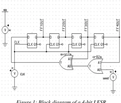
[image:2.612.313.519.145.408.2]to repeat. The missing cycle is due to the lockup state of the feedback pattern [13]. Figure 1 shows the block diagram of a four-stage Fibonacci implementation. Since only two taps are required to configure the LFSR for maximum sequence length, a single XOR are used in the feedback path to perform the modulo-2 summation.
Figure 1: Block diagram of a 4-bit LFSR
In this 4-bit LFSR shown, there are 24-1 or 15
states in the sequence. XOR gate were used in the feedback path, which does not allow them all 0 state, the unique values of the resulting sequence with a starting seed of 1,0,0,1 is shown in table 1. As the number of stages in the LFSR increases, it will affect the number of possible configurations of the feedback network to achieve a maximum length sequence. Each of these different configurations results in a different sequence generation [14]. If more feedback taps are used, then the equation to model the sequence becomes more complicated and thus the resulting maximum length sequence will be more complicated. The number of possible ways to
[image:2.612.94.293.381.550.2]configure the feedback as well as the number of taps used varies especially enlarger LFSRs [15].
Table 1: Unique values for a 4-bit LFSR
In this research LFSR layout was designed by using 3 differences D-flip-flop technique and components such as NAND gates, Pass Transistor and Transmission gates. Mentor Graphics tools are used to design layout for D flip-flop and LFSR. In this research CEDEC KIT is used which is an IC design tools that enable to prepare an IC design which qualifies to be fabricates using Silterra 0.18µm CMOS process.
2.1 D Flip-Flop Design using NAND Gate
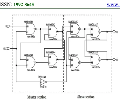
A master slave D flip-flop is created by connecting two gated D latches in series, and inverting the enable input to one of them. It is called master slave because the second latch in the series only changes in response to a change in the first (master) latch [16]. A D flip-flop takes only a single input, i.e. D (data) input. The master-slave configuration has the advantage of being edge-triggered, making it easier to use in larger circuits, since the inputs to a flip-flop often depend on the state of its output. Master slave D flip-flop construction using Mentor graphics design architecture IC (DA-IC) is shown in figure 2. The circuit consists of two D flip-flops connected together. When the clock is high, the D input is stored in the first latch, but the second latch cannot change state.
Clock FF1_O UT FF2_O UT FF3_O UT FF4_O UT
1 1 0 0 1
2 1 1 0 0
3 0 1 1 0
4 1 0 1 1
5 0 1 0 1
6 1 0 1 0
7 1 1 0 1
8 1 1 1 0
9 1 1 1 1
10 0 1 1 1
11 0 0 1 1
12 0 0 0 1
13 1 0 0 0
14 0 1 0 0
15 0 0 1 0
Figure 2: D Flip-Flop schematic using NAND gates
When the clock is low, the first latch's output is stored in the second latch, but the first latch cannot change state. The output can only change state when the clock makes a transition from high to low. Based on this theory, this research is designed several type of D-flip-flop. By designing it, comparison and analysis can be sustained in order to find circuits with less MOS for low power application. Layout of this D flip-flop using NAND gates before implemented at LFSR is shown in figure 3.
We are unable to place the figure here due to its size, which is placed at the below of the manuscript
Figure 3: D Flip-Flop layout using NAND gate
2.2 D Flip-Flop Design using Transmission gate
This flip-flop is realized by using four transmission gate based latches operating on complementary clocks [17]. Several varieties of the transmission gate based are available. For example, the feedback transmission gate may be eliminated or even PMOS transistors may be removed for transmission gates. However, in this research the simulation will only consider typical transmission gate based latch as shown in figure 4. The edge-triggered flip-flop is built from two D-type level-triggered latches. Both latches are enabled with opposite polarity of the clock signal. The second (or
slave) latch is controlled by the clock signal, while
the first (or master) latch is enabled by the negated clock [18].
We are unable to place the figure here due to its size, which is placed at the below of the manuscript
Fig 4: D Flip Flop schematic using transmission gate
As a result of this wiring of the clock signal, the first latch is transparent while the clock signal is low, and the current value of the D input is propagate to the input of the second latch.
However, the input t-gate of the slave latch is non-conducting. Therefore, the flip-flop stores its current value (regenerated via the feedback loop of the slave latch). On the rising edge of the input clock, several things happen. First, the input t-gate of the master latch becomes non-conducting, while the feedback t-gate of the master latch becomes conducting. That is, the master latch stores its current value - the value it had immediately before the rising-edge of the clock signal. At the same time, the slave latch becomes transparent (its input t-gate is now conducting) and therefore outputs the value stored in the master latch. The new output value arrives at the Q output about three transistor delays (slave input t-gate, two inverter stages) after the rising edge of the clock signal [19].
When the clock signal turns low again, the input t-gate of the slave latch becomes non-conducting, while the feedback t-gate becomes conducting. That is, the slave latch keeps storing its current value, namely the value loaded during the preceding rising-edge of the clock signal into the master latch. At the same time, the master latch becomes transparent again and the D input value is propagated through the master latch onto the (now non-conducting) input t-gate of the slave latch [20]. Layout of this D Flip-Flop using transmission gate before implemented at LFSR is shown in figure 5.
We are unable to place the figure here due to its size, which is placed at the below of the manuscript
Figure 5: D Flip-Flop layout using Transmission gate
2.3 D Flip-Flop Design using Pass Transistor
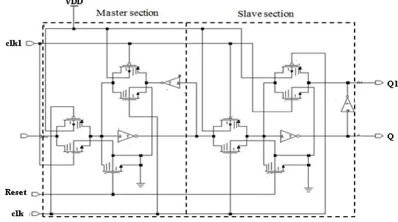
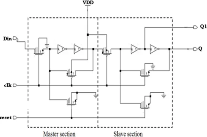
Figure 6 show the most ideal of edge trigger latch that designed using pass transistor and inverter. This is done by configuring two D latches in master slave configuration. A master slave D flip-flop is created by connecting two gated D latches in series, and inverting the clock input to one of them. It is called master slave because the second latch in the series only changes in response to a change in the first (master) latch [21].
We are unable to place the figure here due to its size, which is placed at the below of the manuscript
Figure 6: D Flip Flop schematic using pass transistors
unaffected by the changes in D because it is now hindered by the second level of pass transistor. Thus, we observe that Q remains unchanged for the entire clock cycle and changes only at the positive edge [22]. Hence, the above transistor level diagram implements positive edge triggered flip-flop. Layout of this D flip-flop using pass transistor before implemented at LFSR is shown in figure 7.
We are unable to place the figure here due to its size, which is placed at the below of the manuscript
Figure 7: D Flip-Flop layout using pass transistors
3. RESULTS AND DISCUSSION
Conventional Integrated circuit design is becoming more complex every day. IC station is used to create the layout for the D flip-flops. These processes have been done after designing schematic and verified it using Mentor Graphics DA-IC. Layout versus Schematic (LVS) is a tool in IC Station that links an IC layout to a DA schematic sheet. The layouts of D flip-flop using difference architecture were implemented in this research.
[image:4.612.88.305.485.621.2]By using mentor graphics tools, layout size can be measured. This software also applied for calculate power consumption and quantity of transistor in the layout. The comparison chart of the D flip-flop in terms of number of transistor, power consumption and layout area are shown in table 2. According to table 2, it is being shown that both the layout area and power consumptions are minimal while pass transistor is used.
Table 2: D flip-flop comparison using difference architecture
Component No. of Transistor Power Consumption (piko watt) Layout Area (micro sq. meter)
NAND gates 34 1463.1 409.5
Transmission
Gate 18 742.6332 312
Pass
transistor 14 570.5188 241.8
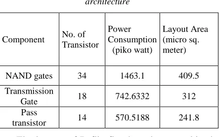
The layouts of D flip-flop have been combined to make LFSR and the comparison between LFSR using NAND gate, transmission gate and pass transistor is shown in table 3. All these layouts are implemented using 0.18µm CMOS technology. Number of transistors, power consumption and layout area of D flip-flop and LFSR is varied in difference technologies. According to table 2 and table 3 the power consumption is much lower if pass transistor is used to design DFF and LFSR.
The layout area also minimized if pass transistor is used for designing D flip-flop and LFSR.
Table 3: LFSR comparison using difference architecture
Component No. of Transistor Power Consumption (nano watt) Layout Area (micro sq. meter) NAND
gates 154 683.50 1808.04
Transmissio
n Gate 90 1523.7 1430
Pass
transistor 74 3.1049 1137.76
4. CONCLUSION
This paper describes how D flip-flop design is important to get low power application for LFSR. By comparing LFSR design using NAND gate, transmission gate and pass transistor, the research showed that, pass transistor have smallest power consumption which is 3.1049 nano watt. This also applies to number of transistor and layout area, which is 74 and 1137.76 micro square meter respectively. Thus, pass transistor is the most efficient method that can be used to design LFSR.
REFRENCES:
[1] M. Kalaiselvi and K.S. Neelukumari, “LFSR-reseeding scheme for achieving test coverage”, in Proc. of International Conference on Information Communication and Embedded Systems, Chennai, India, February 21- 22, 2013, pp. 1209-1213.
[2] F. Mohd-Yasin, M. K. Khaw, and M. B. I. Reaz, “Radio frequency identification: Evolution of transponder circuit design”, Microwave Journal, Vol.49, No.6, 2006, pp. 56-70.
[3] J. Uddin, M. B. I. Reaz, M. A. Hasan, A. N. Nordin, M. I. Ibrahimy, and M. A. M. Ali, “UHF RFID antenna architectures and applications”, Scientific Research and Essays, Vol.5, No.10, 2010, pp. 1033-1051.
[4] Y. K. Teh, F. Mohd-Yasin, F. Choong, M. I. Reaz, and A. V. Kordesch, “Design and analysis of UHF micropower CMOS DTMOST rectifiers”, IEEE Transactions on Circuits and Systems II: Express Briefs, Vol. 56, No. 2, 2009, pp. 122-126.
Lumpur, Malaysia, December 6-9, 2010, pp.168-171.
[6] F. Mohd-Yasin, M. K. Khaw, and M. B. I. Reaz, “Techniques of RFID systems: Architectures and applications”, Microwave Journal, Vol. 49, No. 7, 2006, pp. 62-74. [7] M. K. Khaw, F. Mohd-Yasin, and M. I. Reaz,
“Recent advances in the integrated circuit design of RFID transponder”, in Proc. of IEEE International Conference on Semiconductor Electronic, Scotland, UK, May 23-28, 2004, pp. 326-330.
[8] L. Feng, X. Wang, and Y. Fang, “An Improved Algorithm of Stream Cipher Based on LFSR”, in Proc. of 8th International Conference on Wireless Communications, Networking and Mobile Computing, Shanghai, China ,September 21-23, 2012, pp. 1-4.
[9] M. J. Rani and S. Malarkkan, “Design and Analysis of a Linear Feedback Shift Register with Reduced Leakage Power ˮ, International Journal of Computer Applications, Vol.56, No.14, 2012, pp.9-13.
[10] W. Aloisi and R. Mita, “Gated-Clock Design of Linear-Feedback Shift Registers”, IEEE Transactions on Circuits and Systems II: Express Briefs, Vol. 55, No. 6, 2008, pp. 546 - 550.
[11] R.S. Katti, X. Ruan, and H. Khattri, “Multiple-output low-power linear feedback shift register design”, IEEE Transactions on Circuits and Systems I: Regular Papers, Vol. 53, No.7, 2006, pp.1487-1495.
[12] H. Lv, Jian-Xia Xie, Jun-Chu Fang, and P. Qi, “Generating of a nonlinear pseudorandom sequence using linear feedback shift register”, in Proc. of International Conference on ICT Convergence, Jeju Island, Korea, October 15- 17, 2012, pp. 432 - 435.
[13] H. S. Kim and S. Kang, “Increasing encoding efficiency of LFSR reseeding-based test compression”, IEEE Transactions on Computer-Aided Design of Integrated Circuits and Systems, Vol. 25, No. 5, 2006, pp. 913 – 917. [14] S. Krishnaswamy and H.K. Pillai, “On the
Number of Linear Feedback Shift Registers With a Special Structure”, IEEE Transactions on Information Theory, Vol. 58, No.3, 2012, pp. 1783-1790.
[15] J. Lin, S. Chen, and Y. Hu. “Cycle-Efficient LFSR Implementation on Word-based Micro-architecture”, IEEE Transactions on Computers, Vol. 62, No. 4, 2012, pp. 832 - 838.
[16] V. Marudhai, “Implementation of LFSR on ASIC”, in Proc. of Annual IEEE India Conference, Kochi, India, December 7-9, 2012, pp. 275-279.
[17] N. A Doshi and S.B Dhobale, “LFSR Counter Implementation in CMOS VLSI”, in Proc. of World Academy of Science, Engineering and Technology, Kuala Lumpur, Malaysia, 2008, pp. 942-946.
[18] N. Mukherjee, J. Rajski, G. Mrugalski, A. Pogiel, and J. Tyszer, “Ring Generator: An Ultimate Linear Feedback Shift Register”, Computer, Vol. 44, No.6, 2011, pp. 64-71. [19] P. Murali and G. Senthilkumar, “Modified
Version of Playfair Cipher Using Linear Feedback Shift Register”, in Proc. of International Conference on Information Management and Engineering, Kuala Lumpur, Malaysia, April 3-5, 2009, pp. 488-490.
[20] D. Muthiah and A. Arockia Bazil Raj, “Implementation of high-speed LFSR design with parallel architectures” , in proc. of International Conference on Computing, Communication and Applications (ICCCA), Tamilnadu, India, Feb 22-24, 2012, pp. 1-6. [21] V. Sidorenko, G. Richter, and M. Bossert,
“Linearized Shift-Register Synthesis”, IEEE Transactions on Information Theory, Vol. 57, No. 9, 2011, pp. 6025-6032.
Figure 3: D Flip-Flop layout using NAND gate
[image:6.612.112.499.383.599.2]Figure 5: D Flip-Flop layout using Transmission gate
[image:7.612.141.475.412.633.2]