14th International Conference on Wireless Communications, Networking and Mobile Computing (WiCOM 2018) ISBN: 978-1-60595-578-0
A Design of Real-Time Clock for Wireless Communication
SoC in Smart Grid
Yingying Chi1,2,* and Zhe Zheng1,3
ABSTRACT
This paper presents a real-time clock (RTC) designed for wireless communication system-on-chip (SoC) in smart grid. The RTC is a high-density integrated application-specific circuit using high-precision crystal oscillator as the clock source to keep track of time and date information. The accuracy of travel time makes it very suitable for all occasions requiring low power consumption and accurate timing. The front-end design is implemented with Verilog HDL, and the back-end design and verification are performed with Synopsys` EDA tools.
INTRODUCTION
A real-time clock device is an application-specific integrated circuit that provides functions such as calendar/clock, timing and data storage. It is often used as a clock source and parameter-setting storage circuit for various computer systems. RTC is characterized by accurate timing, low power consumption, and small size. It is especially suitable for recording the time and related information of events occurring in various embedded systems, such as communications engineering, power automation, and industrial control. With the continuous development of integrated circuit technology, new devices with RTC are also being introduced. These new products, not only have accurate real-time clock but also have large-capacity memories, temperature sensors, and A/D data acquisition channels, have been applied in the embedded systems with a microcontroller as the core[1].
The proposed RTC in this paper can provide accurate current time organized as year, month, day, hour, minute and second for the embedded processor. When the main power supply of the system is powered off, the RTC is powered by the backup battery; when there is no battery backup, the registers of the real-time clock generator are cleared after the power is turned off, therefore the real time data is required for calibration after the power is reapplied[2]. The proposed RTC is a time
1
tick generator, a calendar clock organized as year, month, day, hour, minute, and
1
Global Energy Interconnection Research Institute Co.,Ltd. 2
State Grid Key Laboratory of Information & Network Security 3
State Grid Laboratory of Electric Power Communication Network Technology, Beijing, China
second in BCD code, a timing alarm for alarm interruption or wake-up from a power failure mode, and also a leap year generator.
SYSTEM ARCHITECTURE
Architecture
The RTC structure is shown in Figure 1. It is mainly composed of a clock frequency division module, a register control module, a reset signal processing module, and a clock generation module. The register control module includes clock control, interrupt control, interrupt enable control, interrupt status control and address decode control. The clock generation module can perform functions such as calendar clock, timing alarm, leap year calculation and so on.
Functional Modules
As shown in Figure 2, the top-level module rtc_top is connected to the MCU SFR bus via the bus interface module rtc_biu. As seen in the external interface description of the RTC top-level module in Table I, both the read and write enable signals are active low, which means that the bus is allowed to be idle.
The APB wrapper is a conversion component of the AMBA APB protocol and the MCU SFR bus protocol.
Oscillator
Sampling Timer
Interrupt Control
Clock Control Interrupt
Enable Interrupt
Status
Bus Decoder RTC_INT
Address Data Bus Control
Second Minute Hour Day Month Year Time Tick Time_Tick
Reset Register
Calendar Clock Generator Frequency
Divider
Leap Year Generator
[image:2.612.105.494.430.626.2]Second/Minute/Hour/Day/Month/Year Latch
The rtc_top is the top level of the proposed RTC, which merely instantiate the functionality of two modules, rtc and rtc_biu. The rtc module is the core component which works in the RTC clock domain and consists of the main logic and configuration registers of the RTC. The rtc_biu is a bus interface which provides the appropriate MCU clock domain for RTC and it includes bus interface and high-speed pulse units. When writing the time setting value or RTC calibration data, write protection is required first by writing a specific password register, and then the data to be configured is written into rtc_biu. After all the configuration data is written into the rtc_biu module, the write protection is resumed. If the write data is valid, it will be written to the RTC at the same time; if the write data is illegal, an error interrupt will be triggered and the write will be invalid. The RTC internal register status remains unchanged.
The rtc_time module is a group of registers for implementing and maintaining the RTC, including the year/month/day/hour/minute/second registers and the correction register. The module updates the internal registers when a second carry occurs, that is, one cycle width second pulse, or when setting RTC data. Cases where the internal registers need to be updated include writing configuration data, time accumulating and carry. Through the clock gating design, this module works at 1Hz frequency.
According to the configuration data, the rtc_cfg module determines whether the current data value or the configuration value is written in the time data register, and also it determines whether the value in the time data register is valid. If not, the current value is used as the write value instead of the configuration value.
The handshake module rtc_hs implements a handshake with the rtc_biu module and generates a read/write signal to the rtc. When a write operation and a second carry occur at the same time, the carry process has a higher priority, which means that the write signal needs to be delayed.
When the bus initiates a read RTC time operation, the read cache module rtc_rb latches the time data to prevent the second carry from occurring while the bus reads the time register sequentially.
rtc_top
APB
wrapper rtc
rtc_time
rtc_rb
rtc_hs
rtc_itr
rtc_cnt_ocs
rtc_cfg rtc_biu
MCU SFR Interface APB
[image:3.612.154.443.518.649.2]The second counting module rtc_cnt_osc counts the OSC clock and generates a second pulse with a OSC width. The OSC cycle is about 30uS, so the adjustment step per second is 30ppm. In order to increase the compensation resolution, compensation is performed at 29th second and 59th second, that is, the compensation is performed every 30 seconds, and the compensation accuracy can be increased to 1ppm. The compensation method uses a 14-bit complement configuration data named cal. The compensation value is cal-1. So, if no compensation is needed, the cal value should be 1. Normally, the counter is calibrated every 30 seconds, that is, the correction value is added or the correction value is subtracted every 30 seconds. In this design, the correction value lookup table directly stores the accurate count value at a certain temperature, and the correction value is directly assigned to the counter when correcting. Thus, the complexity of the compensation logic can be minimized by avoiding the use of a 14-bit adder.
[image:4.612.105.492.467.683.2]The interrupt management module rtc_itr manages the RTC interrupts, including timer interrupts and error interrupts. Error interrupts include interrupts caused by writing configuration data when write protection is not released and interrupts caused by writing illegal configuration data. The timer interrupt is actually a time information interrupt. The RTC timer interrupt interval setting is shown in Table Ⅱ. When rtc_itr is 111, sec_itv[6] decides whether to use the second counter interrupt, which is active high. The second counter is a counter with a count range of 0~sec_itv[5:0] and a count step length of 1 per second. Its time period is 0~63 seconds; therefore it can generate a timer used in low-power modes with a timing range from 1 second to 1 minute.
TABLE I. Interface of RTC.
Categor
y Name I/O Description
Global Signals
clk I system high-speed clock
clk_rtc I RTC clock, 32768Hz oscillator
rst_n I bus interface asynchronous reset
rtc_rst_n I RTC core asynchronous reset
se I boundary scan enable
Bus Interface
Signals
madr[7:0
] I bus address
mwr_n I write enable
mrd_n I read enable
mdin[7:0
] I data input
mdout[7:
Interrupt Signals
rtc_sp O 1Hz, 50% duty cycle, a periodic interrupt
source or wake-up signal
rtc_intr O RTC timer interrupt pulse signal
rtc_ille_i
tr O RTC error interrupt
Others
sp_i I external pulse input
pll_div_
[image:5.612.104.491.86.199.2]o O system clock frequency output
TABLE II. RTC timer interrupt interval setting.
rtc_itr Interrupt Interval
000 1 second
001 1 minute
010 1 hour
011 1 day
100 0.5 second
101 0.25 second
110 0.125 second
111 0.0625 second
Main Features
The main features of the proposed RTC such as write protection, data configuration/reading, cross-clock handshake, high-frequency counts and calibration are described in detail.
Write Protection
RTC`s internal registers. The situation in which the write protection is lifted is hereinafter referred to as CE.
RTC Data Configuration and Reading
The data delivered by the bus is first cached and then written in parallel to the RTC`s internal registers at the same time. This can avoid both bus wait and the risks associated with writing time information sequentially. The configuration data to be cached includes time information like year, month, day, hour, minute and second. On the rise edge of the CE signal, the time data is all set to 1, which is a special invalid clock data used to indicate that the information has not been modified. After that, the bus writes part or all of the time data one by one. At the falling edge of CE, configuration data is written to the RTC by shaking hands.
Reading time data from RTC also requires synchronization and caching. When the read operation of the data register is initiated, the RTC latches all the time data first, and then the bus can read out the required data one by one.
Cross Clock Handshake
Both the read and write of the RTC time data by bus are cross-clock domain operations. The read operation is initiated by reading the data register and the write operation by dragging CE down. Handshake operation can make the data be read and written after stabilization, which ensures the reliability of the read/write operation. In order to ensure that the handshake is correct, CE`s high level should maintain at least 3 OSC clock widths, that is, 100us.
High-frequency Counter
The high-frequency counter is designed based on a 24-bit counter and a 24-bit threshold register. It has two modes of operation, which can be configured by the state register of the high-frequency counter.
Mode 1 is the frequency divider mode. Whenever the counter counts to the preset threshold value referred as div_pll, the counter returns to zero and flips the output signal, therefore a divided signal whose frequency is fsys/(2·(div_pll+1)) can be obtained. When frequency of the input system clock is 3.2MHz, a second pulse with high resolution is obtained, and the calibration is performed every second by rewriting the frequency division coefficient div_pll according to the temperature. By default, the system clock is divided by 2 and the corresponding division coefficient is equal to zero. The system clock can be divided by 225 maximum.
pulse again, and divides the count value by 2 to the threshold div_pll, so that the width of the external seconds pulse can be recorded and the threshold can be automatically learned to get accurate second division. In state 3, the state is maintained and the counting stops.
Calibration
RTC calibration can be achieved using high-frequency second pulse or temperature compensation.
When using the high-frequency second pulse for correction, the user writes a div_pll value in the frequency division threshold register, and the following relationship exists between the frequency of the high-frequency second pulse and the current system clock:
2
fSYS× (div_pll + 1) = 1
fSP (1) Among them, fSYS is the current system clock frequency, and fSP is the frequency of the high-frequency second pulse when the frequency division threshold is div_pll.
Since fOSC= fSYSK , where K is the multiplier coefficient of the PLL. Substitute it to get fOSC :
fOSC=K2× (div_pll + 1) × fSP (2) The RTC correction is performed at an OSC clock frequency of 32768Hz. The calibration occurs every 30 seconds and the value of the RTC correction register is updated every 30 seconds too. The value of the correction register is referred as C, and the average period is:
T =
1
fOSC×32768×29+ 1
fOSC×(32768+C−1)
30 =
1
fOSC× (32768 + C−1
30) (3) When the system works at the frequency of fSYS = K ∙ fOSC, the value of the high-frequency division threshold register referred as div_pll is TH0. The frequency of the high-frequency second pulse measured via the pin is fSP0. The following equation can make T in equation (3) equals to 1.
C = [2
K× (TH0 + 1) × fSP0− 32768] × 30 + 1
= [2
K× (
fSYS
2 − 1 + 1) × fSP0− 32768] × 30 + 1
time. Temperature measurement circuit principle is shown in Figure 3 and the RTC temperature compensation principle is shown in Figure 4.
Temperature
Sensor ADC
[image:8.612.128.473.135.212.2]Signal Process
Figure 3. Temperature measurement block diagram.
Measure Temperature
Obtain the compensation value of RTC at the current temperature according to the temperature curve
Modify the value of the correction register
Figure 4. RTC temperature compensation principle.
When measuring temperature, put the RTC device into the temperature-controlled box, adjust the temperature-temperature-controlled box from -40°C to 80°C, read the values from the temperature sensor in turn. By recording, we can see that the value read from the register is linear with the actual temperature value, the slope is basically the same, but the constant term is biased.
Four RTC-containing devices (such as a power meter) are placed in a temperature-controlled box, and the temperature-controlled box is adjusted from -40 to 80°C. The crystal frequency of the pin output is measured in turn using a frequency meter. It can be seen from the record that the frequency of the crystal oscillator is parabolic to the temperature. The coefficient deviation between different devices is very small and only the constant term is biased.
The corresponding RTC correction value at each temperature can be calculated by the following method and made into a table for query. First, take the frequency of the crystal oscillator at which the second pulse output is exactly one second as a reference, like 32768Hz. Then the measured crystal frequency x is compared with the reference value, and the correction value y is calculated by the following equation:
[image:8.612.185.406.269.359.2]the value of (1FFF − y) to the correction register; if y < 0, write y to the correction register to calibrate the clock.
Verification
RTC's functional tests are performed using bus operation test sequences, including normal travel/read time test, time legal setting test, timer interrupt test, correction value setting test, illegal time setting test, write protection collision test, high-speed frequency division test and external pulse width count test. It should be noted that the address of the data configuration and data reading are the same, but correspond to different registers. The configuration register is a write only register while the reading register is a read only register, both of which share the same address.
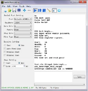
[image:9.612.210.384.279.459.2]18
Figure 5. RTC time information setting and reading.
Use EJTAG to connect to the chip test board and connect the serial debugging tool via RS232. Configure the time information for RTC, read the time data and compare it with the written value. Reset the chip test board, as shown in Figure 5, the result indicates that the RTC is working properly.
Conclusion
alarm for alarm interruption or wake-up from a power failure mode, and a leap year generator.
References
1. https://wenku.baidu.com/view/108938e6d15abe23482f4d4d.html.
2. Dong-Soo Lee, Sung-Jin Kim, etc., “A Design of Fast-Settling, Low-Power 4.19-MHz
Real-Time Clock Generator with Temperature Compensation and 15-dB Noise Reduction,” IEEE Transactions on Very Large Scale Integration (VLSI) Systems, 2018, pp. 1151-1158.
3. Wolfgang Gut, Gerald Hilber, etc., “Low power Real Time Clock with high accuracy over large
supply voltage range,” Norchip 2012, pp. 1-4.
4. Ying-Wen Bai, Hsiao-Chung Chen, “An adjustable design for the Real Time Clock of high-end
server systems,” Canadian Conference on Electrical and Computer Engineering, 2008, pp. 183-188.