32
Static Phase Range Enhancement of Reflectarray Resonant Elements
M. F. M. Shukri and M. Y. Ismail,
Abstract
-There has been much interest
recently in developing reflectarray antenna
due to the combination of some of the best
features between the parabolic reflector and
phased array antennas. This paper presents
the study of the relationship between
phasing distribution characteristics and the
bandwidth of different resonant reflectarray
elements. The gradient characteristics of
different elements of patch, dipole and ring
printed on a grounded dielectric substrate
have been investigated at X-band frequency
range using CST computer model. The
preliminary simulated results generated from
CST computer model demonstrate that ring
elements contribute the highest reflection
loss performance of 1.74 dB compared to
the other two element of dipoles and
patches. The attainable static linear phase
range of 177
ofor ring elements is shown to
offer a trade off between the static phase
range and the bandwidth of the reflectarray
elements.
Keywords: Reflectarray, Phase Range, Resonant Elements
I. INTRODUCTION
A microstrip reflectarray consists of a flat array of microstrip patches or dipoles printed on a thin dielectric substrate [1]. The incident signal illuminating from feed antenna to the array elements to scatter the incident field with the proper phase required to form a planar phase.
This work was supported in part by Research and Management Center of Universiti Tun Hussein Onn Malaysia.
M. F. M. Shukri and M. Y. Ismail are with Universiti Tun Hussein Onn Malaysia, Batu Pahat, Johor. (phone: 4538339; fax: 07-4536060 ; e-mail: [email protected]).
Many types of resonant elements can be used in printed reflectarray antenna depending on its applications. For examples variable size patch elements [2], [3], spiral patch element [4], cross dipole elements [5], [6] and ring elements [7], [8]. The applications were such as dual frequency [7] and for the solar panel reflectarray [5]. There are some feeding method that can be used such as prime-focus feeding, offset feeding and cassegrain feeds [1]. Feed horn is usually used and situated at its focus. This feeding can eliminates the complexity and losses of a microstrip feed. In this project the phasing distribution characteristics will be analyzed using different resonant elements. The operating frequency used for this project will be in X band frequency range (8-12 GHz).
II. THEORY
A. Reflectarray antenna
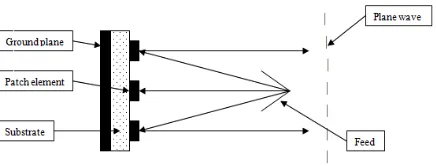
[image:1.612.325.543.494.577.2]Due to the introduction of the printable microstrip antennas, the technologies of combining the reflectarray and microstrip radiators were investigated [9].
Figure 1: Geometry of the microstrip reflectarray.
A feed antenna illuminates the array whose individual elements are designed to scatter the incident field with the proper phase required to form a planar phase surface in front of the aperture, as suggested in Figure 1. The bandwidth performance of a reflectarrray is no match to that of a parabolic reflector. For a printed microstrip reflectarray, its bandwidth is primarily limited by two factors that are
Proceedings of MUCEET2009
Malaysian Technical Universities Conference on Engineering and Technology June 20-22, 2009, MS Garden,Kuantan, Pahang, Malaysia
33
narrow bandwidth of the microstrip patch elements on the reflectarray surface and the differential spatial phase delay [10]. The path length from the feed to all patch elements is all different. This leads to different phase delays. In order to compensate for the different path length, the elements must have corresponding phase advancements design.B. Scattering parameter, S11
The scattering parameter, S11 is referring to
[image:2.612.349.532.181.262.2]reflection loss of the antenna in which the reflection loss of a reflectarray antenna should be 0 dB at resonance in order to get a maximum reflected energy
.
Figure 2: Simulation of S11 variation.
Minimum reflection loss can be achieved as shown in Figure 2 when the signal energy reflection is the same as when signal energy is illuminated.
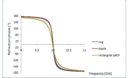
C. S-shaped phase curve plots
[image:2.612.76.293.264.328.2]The slope of the phase versus frequency is a measure of the bandwidth of reflectarray as a curve with a smaller slope will lead to less phase error [1]. There is tradeoff between phase range and the bandwidth. This is indicated by the gradient of the S-shaped phase curve.
Figure 3: Reflection phase versus frequency.
To provide a suitable compensation for all the elements in array, the phasing range needs to be close to 360° at a given frequency [11]. At 180° phase difference, resonant frequency is achieved due to maximum reflection of the signal.
D. Differential Spatial Phase Delay
The differential spatial phase delay, ∆S is the phase difference between the two paths S1 and S2
[image:2.612.75.280.522.605.2]from the feed to the reflectarray elements. The differential spatial phase delay is due to the different lengths from the feed to each point on the wave front of the radiated beam [12].
Figure 4: Differential spatial phase delay of reflectarray [12].
Bandwidth in large reflectarrays, as in the case of space applications, is drastically reduced because of the different path length. The different lengths from the feed to each patch location, which is compensated by the reflection coefficient to produce a reflected field with progressive phase [9].
E. Phase Delay
Phase errors can be introduced by fabrication tolerances in flatness of array and etching of elements [1]. Phase errors can also be introduced by the feed antenna if its phase center is not well-defined [13]. Phase errors related to the changes in patch size [14].
III. METHODOLOGY
A. CST Computer Model Simulations
Analysis has been done with the results in order to observe the parameters of the simulation results. The parameters such as S11 and S-shaped
phase curve have been investigated. Apart from that, the current distribution parameter also carried out.
[image:2.612.339.525.601.693.2]
34
B. Fabrications of AntennasFrom the results CST computer model simulation fabrications of different resonant elements have been carried out. There are several stages in fabrication process that required producing the antennas. The fabrication process was prepared using facilities in UTHM PCB laboratory and using the material supplied. The material for substrate is Rogers RT5870 with dielectric constant, εr 2.33 and
dissipation factor, tan δ 0.0012. The fabrications processes include three steps:
a) Dry Film Lamination
Substrate board was cut to match with the size of patch elements.
1. The film laminator machine was set to preheat.
2. Substrate board was placed into laminator machine.
b) UV Exposure
1. The film of patch layout was attached to the laminated substrate board.
2. The substrate board was placed under UV exposure around 2 minutes.
3. The film was taken off and can be seeing printed on the surface of the substrate board.
c) Etching Process
i. Photo Resist Developer
1. In this process laminator film was vanished.
ii. Copper Etching and Resist Strip
1. In copper etching process unwanted copper remove by Etching Machine.
2. The unwanted surface substrate board was placed into Spray Stripping Machine.
3. PCB Dryer Machine used to dry up the substrate board.
IV. RESULTS AND DISCUSSIONS
Simulations have been done using CST computer model in order to study the scattering behaviour of resonant elements of reflectarray. Measurements have been performed using the waveguide simulator technique as it is able to measure the scattering matrix of an infinite array of resonant elements.
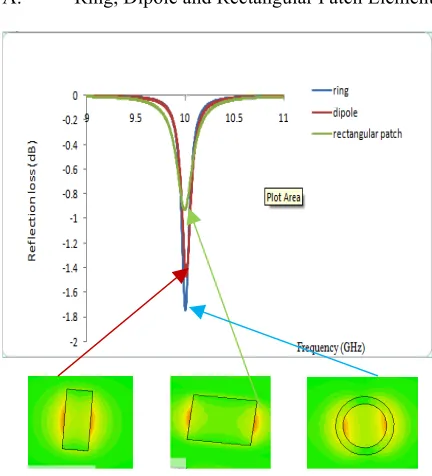
[image:3.612.323.539.80.318.2]A. Ring, Dipole and Rectangular Patch Element
Figure 6: Scattering parameter of ring, dipole and rectangular patch elements
(ring element dimensions: outer radius= 3.97 mm and inner radius= 2.97 mm; dipole element, w = 3.74 mm and 8.6 mm and rectangular patch element, w = 11.62 mm and l = 8.5mm)
Simulated results generated from CST computer model demonstrate that ring element is shown to have higher loss compared to dipole and rectangular patch element. The significant change in the loss performance of the ring element is due to the small area of the ring element compared to dipole and rectangular patch elements. Because of this, ring element has a higher loss and less bandwidth compared to dipole element and rectangular patch element [1]. This is clearly shown by the surface current distribution generated from the CST computer model.
35
Figure 7: Measured and simulated results of ringElement
[image:4.612.329.535.170.297.2]
Figure 8: Measured and simulated results of dipole element
Figure 9: Measured and simulated results of rectangular patch
From Figure 7,8 and 9 show the scattering parameter results for three different elements of dipole, square patch and ring. The ripples demonstrated in the plots are due to the mismatched of the calibrations. The cable connected to the vector network anylzer should have been calibrated properly to get scatrering parameters of S11. The dimensions of
patch fabrication also has effected. Similar with S-shaped phase curves in previously, ring element contribute a wider phase range compared to other two elements. Dipole element nearly same as ring element has wider phase range. Bandwidth for ring
element can be increased by a suitable choosing the outer and inner radius ratio [7].
Table 1 shows the linear phase range and Figure of Merit for three resonant elements. Both wider linear phase range and larger Figure of Merit contributed by ring element followed by dipole and rectangular patch elements.
Figure 10: Combination of ring, dipole and rectangular patch element in S-shaped phase curve.
[image:4.612.69.294.174.304.2]
Table 1:Figure of Merit (FoM).
The significant difference in the static phase range is primarily due to the trade off between narrow bandwidth and greater linear phase range.
V. CONCLUSIONS
[image:4.612.314.537.350.449.2]36
ACKNOWLEDGMENT
The author would like to thank Universiti Tun Hussein Onn Malaysia for providing the equipment and materials.
REFERENCES
[1] D. M. Pozar, S. D. Targonski and H. D. Syrigos, “Design of
Millimeter Wave Microstrip Reflectarrays,” IEEE Trans. Antennas
Propag., vol. 45, no.2, 1997, pp. 287–296.
[2] H. Rajagopalan and Y. R. Samii, “Dielectric and Conductor Loss Quantification for Microstrip Reflectarray: Simulations and
Measurements,” IEEE Trans. Antennas Propag., vol. 56, no.4,
2008, pp. 1192–1196.
[3] D. M. Pozar and T. A. Metzler, “Analysis of a Reflectarray Antenna Using Microstrip Patches of Variable Size,” Electron. Letter, vol. 29, no. 8, 1993, pp. 657-658
[4] D. M Pozar and Stephan D. Targonski “Analysis and Design of a Microstrip Reflectarray Using Patches of Variable Size”, IEEE Transactions on Antennas and Microwave Propagation
[5] S. Datthabasombat, A. Prata, Jr, P. Brown and O. Quientero “ Spiral Microstrip Patch Element For Reflecarray.
[6] M. E. Bialkowski, A.M. Abbosh and K. H. Sayidmarie (2008) “Investigations into Phasing Characteristics of Printed Single and Double Cross Elements for Use in a Single Layer Microstrip Reflectarray” IEEE.
[7] D. M. Pozar and Stephen D. Targonski (1998) “ A Microstrip Reflecarray using Crossed Dipoles “, IEEE.
[8] N. Misran, R. Cahill and V.F. Fusco (2002) “ Reflection Phase Response of Microstrip Stacked Ring Elements “Electronics
Letters, No.8, Vol 38.
[9] K. H. Sayidmarie and M. E. Bialkowski (2008) “ Multi-Ring Unit Cells for Increased Phasing Range in Single Layer Microstrip Reflectarrays “ , Proceedings of iWAT.
[10] Vibha Rani Gupta and Nisha Gupta “Gain and Bandwidth Enhancement in Compact Microstrip Antenna”.
[11] Jose A. Encinar and J. Agustin Zornoza (2003) “ Broadband
Design of Three Layer Printed Reflectarrays “, IEEE Transactions
on Antennas and Propagation, No 7, Vol 51.
[12] John D. Kraus and Ronald J. Marhefka (2002) “ Antennas For All Aplications”, McGraw-Hill Higher Eduction.
[13] John Huang, Jose A.Encinar (2008) “Reflectarray Antennas” Institute of Electrical and Electronic Engineers.
![Figure 4: Differential spatial phase delay of reflectarray [12].](https://thumb-us.123doks.com/thumbv2/123dok_us/8781343.904387/2.612.339.525.601.693/figure-differential-spatial-phase-delay-reflectarray.webp)