Technology (IJRASET)
Low Area and Low Power CMOS technology based
RAM and Ternary CAM memory design
V.Raghavendranm1, B.Pushparaj2
II year M.E (Applied Electronics), Assistant Professor / Department of ECE Renganayagi Varatharaj College of Engineering, Salvarpatti, Sivakasi.
Abstract - Ternary content addressable memory (TCAM) is an associative memory or associative array for very high speed searching applications. It compares input search data (tag) against a table of stored data and returns the address of matching data. Several custom computers were built to implement TCAM. In this paper the system proposed an XOR based content addressable memory. Data matching process is applicable to match line sense amplifier (MLSA). Given an input tag the proposed architecture computes a few possibilities for the location of the matched tag and performs the comparisons on them to locate a single valid match. Proposed method is to design the CMOS based RAM and CAM memory architecture design. This design is used to find match line data effectively and to reduce the leakage power level for match line process. The proposed system is mainly focused by the matched line sense amplifier process and to compare the content data between the data register and 4x4 TCAM cell design. Ternary CAM design is used to consume less power and also to reduce the leakage power of CMOS transistors. This design is used to reduce the delay time as well as to increase the speed in ML search process.
Keywords - Content Addressable Memory(CAM), Ternary CAM, XOR type CAM cell, Static Random Access Memory (SRAM), Low Power.
I. INTRODUCTION
Standard computer memory such as random access memory (RAM) in which the user supplies a memory address and the RAM returns the data word stored at that address. TCAM is designed such that the user supplies a data word and the TCAM searches its entire memory to see if that data word is stored anywhere in it [2]. If the data word is found the TCAM returns a list of one or more storage addresses where the word was found. Numerous devices have been produced by Integrated Device Technology, Cypress Semiconductor, IBM, Broadcom and others to the Look-aside interface agreement [6]. Binary CAM is the simplest type of TCAM which uses data search words consisting entirely of 1s and 0s [1]. Ternary TCAM (TCAM) allows a third matching state of "X" or "don't care" for one or more bits in the stored data word thus adding flexibility to the search [2]. For example a ternary CAM might have a stored word of "10XX0" which will match any of the four search words "10000", "10010", "10100" or "10110".
The added search flexibility comes at an additional cost over binary CAM as the internal memory cell must now encode three possible states instead of the two of binary CAM [4]. This additional state is typically implemented by adding a mask bit such as "care" or "don't care" bit to every memory cell. In modern computer memory a sense amplifier is one of the elements which make up the circuitry on a semiconductor memory chip. A sense amplifier is part of the read circuitry that is used when data is read from the memory its role is to sense the low power signals from a bit line that represents a data bit 1 or 0 stored in a memory cell and amplify the small voltage swing to recognizable logic levels so the data can be interpreted properly by logic outside the memory [2]. Modern sense amplifier circuit consists of two to six usually four transistors [7]. Sense amplifiers for core memory sometimes contained thirteen transistors. There is one sense amplifier for each column of memory cells so there are usually hundreds or thousands of identical sense amplifiers on a modern memory chip. As such sense amplifiers are one of the only analog circuits in a computer memory subsystem. In this paper TCAM refers to binary CAM (BCAM) with don’t care [2]. The CAM array is divided into several equally sized sub blocks which can be activated independently. For a previously trained network and given an input tag the classifier only uses a small portion of the tag and predicts very few sub blocks of the TCAM to be activated. Once the sub blocks are activated the tag is compared against the few entries in them while keeping the rest deactivated and thus lowers the dynamic energy dissipation as well as to reduce the power consumption.
the system design of 6T based static random access memory (SRAM) CMOS design [Fig.4]. This design is to store the single bit value. This design consists of two inverter cross connection is used to maintain the given input data. Then the system design of 8T based XOR Ternary CAM design [Fig.2]. It consists of selection line (SL) and the bit line (BL) to control the TCAM cell. This process used to find the address bit location. Then the scan based enable process is to find the TCAM cell array result. The XOR gate function to match the SRAM data and TCAM data and to invert the activation result. The match line process is to check the CAM data register. The clock function is to control the output matched line row then it will get the content address [Fig.1].
Fig. 1 Proposed system flow diagram If the write line is set to ‘1’, then to get the data to cross inverter circuit connection.
Fig. 2 XOR type Single CAM cell
[image:3.612.173.443.378.630.2]Technology (IJRASET)
Fig. 3 Two-Side Self-Gating Ternary CAM array
[image:4.612.178.424.312.435.2]The scan based enable process is to find the TCAM cell array result and to apply the CAM and RAM data. The XOR gate function to match the SRAM data and TCAM data and to invert the activation result [2]. To check the all the row CAM data to data register input data bit then to activate the ML function.
Fig. 4 Proposed circuit of 6T based SRAM
The match line process is to check the CAM data register and RAM data register value. The clock function is to control the output matched line row and to get the content address [4]. This matched line process is mainly focused by the TCAM cell array input data storage [5]. The final output is to identify the content address effectively and to increase the ML check process time. Then to consider the power consumption level and to check the match line delay time also. Area consumption is depends on optimization of MOS transistors count level.
III. RESULT ANALYSIS
[image:4.612.174.441.571.705.2]simulator.
Fig. 6 Schematic entry of 8T based Ternary CAM design
[image:5.612.181.434.315.474.2]n fig.6 denoted as schematic entry of eight transistors based Ternary CAM memory design using S-Edit of TANNER version 13.0 simulator.
Fig. 7 Schematic entry of 4x1 TCAM array cell
In fig.7 represented as schematic design of 4x1 ternary content addressable memory cell using S-Edit of TANNER version 13.0 simulator.
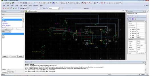
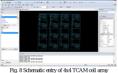
Fig. 8 Schematic entry of 4x4 TCAM cell array
[image:5.612.207.435.509.651.2]Technology (IJRASET)
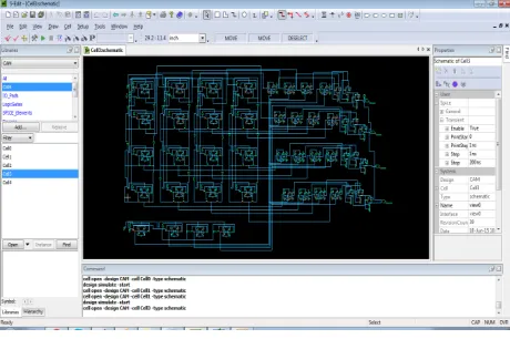
Fig. 9 Schematic entry of 4x4 TCAM with MLSA
[image:6.612.79.510.277.626.2]In fig.9 conclude as a schematic design of 4x4 ternary content addressable memory cell array with match line sense amplifier and scan based enable function using S-Edit of TANNER version 13.0 simulator.
Fig.10 Output - Power consumption of 4x4TCAM
IV. PERFORMANCE COMPARISIONS
Parameters of Simulation (Units) Existing System Proposed System
Supply Voltage (V) 1.8 5
Optimization of MOS transistors count level (~ numbers)
512 400
Power consumption (mw) 94 70
Delay time (ns) 7 2.42
Area consumption (mm^2) 4.83 0.320
V. CONCLUSION
was also implemented in the same process technology.
REFERENCES
[1] Naoya Onizawa, Shoun Matsunaga, Vincent.G.Gaudet, Warren J.Gross and Takahiro Hanyu, Members IEEE, “High Throughput Low Energy Self Timed CAM based on Reordered Overlapped Search Mechanism”, IEEE Transactions on Circuits and Systems-I:Regular papers, Volume 61, No 3, March 2014, pp. 865-876.
[2] Yen-Jen Chang, Kun-Lin Tsai and Hsiang-Jen Tsai, Members IEEE, “Low Leakage TCAM for IP Look-up using Two-Side Self-Gating”, IEEE Transactions on Circuits and Systems-I, Regular papers, Volume 60, No 6, June 2013, pp. 1478-1486.
[3] Salvador Petit, Rafeal Ubal, Julio Sahuquillo and Pedro Lopez, Members IEEE, “Efficient Register Renaming and Recovery for High Performance Processors”, IEEE Transactions on Very Large Scale Integration (VLSI) Systems, Volume 22, No 7, July 2014, pp. 1506-1514.
[4] Anh-Tuan Do, Shoushun Chen, Zhi-Hui Kong and Kiat Seng Yeo, “A High Speed Low Power CAM with a Parity bit and Power Gated ML Sensing”, IEEE Transactions on Very Large Scale Integration (VLSI) Systems, Volume 21, No 1, January 2013, pp. 151-156.
[5] Shun-Hsun Yang, Yu-Jen Huang and Jin-Fu Li, “A Low Power Ternary Content Addressable Memory with Pai-Sigma Match Lines”, IEEE Transactions on Very Large Scale Integration(VLSI) Systems, Volume 20,No 10, October 2012, pp. 1909-1913.
[6] Hooman Jarollahi, Naoya Onizawa, Vincent Gripon and Warren J.Gross, “Reduced Complexity Binary Weighted Coded Associative Memories”, ©2013 IEEE, pp. 2523-2527.
[7] Hooman Jarollahi, Naoya Onizawa, Vincent Gripon and Warren J.Gross, “Architecture and Implementation of an Associative Memory using Sparse Clustered Networks”, ©2012 IEEE, pp. 2901-2904.
[8] Nen-Fu Huang, Whai-En Chen, Jian-Yu Luo and Jun-Min Chen, “Design of Multi-field IPv6 Packet Classifiers Using Ternary CAMs,” ©2001 IEEE, pp. 1877-1881.
[9] Yen-Jen Chang, Member IEEE, “Don’t Care Gating (DCG) TCAM design used in network routing table,” IEEE Transactions on Very Large Scale Integration (VLSI) Systems, Volume 18, No 11, November 2010, pp. 1599-1607.