6
I
January 2018
S-Parameter and Positron Lifetime Studies of Mn
Doped Zn
1-X
o
x
Vandana Rathore1
1
School of Engineering and Technology, Jagran Lakecity University, Bhopal-462044, India.
Abstract: Zinc Oxide (ZnO) is an fascinating material and have potential applications as a transparent conductive electrodes for solar cells, light emmitting diodes as well as for gas sensors. Interaction between dopant, impurities and intrinsic defects plays an essential role to enhance the electrical and optical properties of ZnO thin films. Positron annihilation spectroscopy (PAS) is a non destructive technique to study thin films and nanocrystalline materials. The mechanism of positron annihilation in oxide thin films has been discussed in terms of diffusion of positrons inside the grain boundaries, nanovoids and thermally generated vacancies. The mean positron lifetime and S-parameter as a function of grain size in pure and Mn doped ZnO thin films has been calculated by using positron diffusion model. The samples are prepared by Spray pyrolysis method and temperature dependent measurements revels information about the presence of shallow positron traps like grain boundaries and interfacial defects. The calculations of shows that mean positron lifetime decreases as the grain grows. While the S-parameter increases with the increase in the siza of grains. This increase in
has been ascribed to the increase in the number of thermally generated vacancies at higher temperatures. diffusion can also be closely linked with thermal defect formation at higher temperatures. Thus, information regarding grain boundaries in thin films and nano composites can be gathered by DTM (diffusion Trapping Model).I. INTRODUCTION
II. FORMULATION OF THE DIFFUSION TRAPPING MODEL
The mechanism of positron annihilation in nanocrystalline materials is known to be more complex than that in metals and semiconductors because, a fraction of positrons can form a bound state with an electron. In the following, we consider the case of the slow positrons incident on a thin film having size (50 nm-200 nm). The positron gets rapidly thermalized before annihilation. After slowing down within 10 ps the penetrated positrons either directly annihilate with surrounding electrons or combine with an electron to form positronium. Fractions of positrons may diffuse back to the surface and escape into the vacuum. The positrons and positronium both are known to localize in interfacial defect and nanovoids. The theoretical model is based on diffusion trapping model (DTM). When a beam of moenergetic positron is implanted into a semiconductor surface the following processes have been considered to occur before annihilation. Firstly the positrons may diffuse back to the surface and annihilate as a free particle. Secondaly it may be trapped at a defect site. In the present work, we have considered two types of defects i.e. trapping into shallow defects and in native ion vacancy defects. The rate equations have been setup to describe all the above processes and have been solved to obtain the Doppler broadening line shape parameter or S-parameter as a function of incident positron energy in undoped and ZnO doped with different types of ions. The diffusion trapping model is able to describe the positron annihilation in ZnO thin films and it has been observed that at low energy the Sparameter corresponds to positron annihilation in the surface state and for higher energy the same corresponds to the positron annihilation in the bulk material. In case of ion implanted ZnO the S-parameter was found to be dependent on the concentration of vacancy clusters. The vacancy clusters concentration was found to be related to the atomic number of the implanted ion as well as on the fluency. The three dimensional diffusion equation has been solved and the rate equations are set up to describe the tapping of positrons at interfacial defects and nanovoids. The model has been functional to calculate the mean positron lifetime (
) in pure and Mn-doped ZnO thin films as a function of grain size. It has been also employed to explain the S-parameter configuration in pure and doped ZnO thin films. In the present work, our endeavor is to understand the consequence of positron mean lifetime on grain size and types of defects in nanocrystalline thin films of zinc oxides. In the model considered, we assume that positrons diffuse in the interfacial defects in which they annihilate with annihilation rate of free positrons in the samplef (=1/f). Let C(r,t) is the local positron density with in the grain. The change in the positron concentration inside defects with time and space is described by the three dimensional diffusion equation:
,
) , ( ) , ( ) , ( nv2 n C r t
r t r C t r C D t t r C f
(1)For the present calculation, D+ is the positron diffusion coefficient and C (r,t) is the positron density as a function of both time and position. we assume that at t = 0 the positrons are uniformly distributed and there are no positrons trapped at interfacial defects and nanovoids. Thus, the diffusion equation is solved subjected to the boundary conditions: where V is the volume of the grain having radius R. Thus, we obtain the solution of equation (1). When a beam of monoenergetic positrons is implanted from vacuum into the grain, the positron survives before annihilation either as a free positron or trapped at the grain boundary or into the thermally induced vacancy.
0 n 2 2 3 exp ) 1 2 ( ) , ( t R D R r V n t r C f n (2)In the above equations nfg, nfv represent the fraction of positrons trapped at the grain boundaries and into nanovoids vacancies respectively. nvf represents the fraction that detrapped from vacancy to free state. fg, fv and vf represent the transition rate from free to grain boundary, free to vacancy and from vacancy to free state respectively. g and vare the positron annihilation rate at the grain boundary and into the vacancy respectively. The total number of positrons reaching at the grain boundary is given by
)
,
(
)
(
t
ds
C
r
t
N
fg
(3)The mean positron lifetime (
) in the nanocrystalline samples can be written as: Thus, one gets
0 n nn 1 1
b B 1 v g fv vf g fv g g
g
In case of thin films the Doppler broadening line shape parameter or S parameter would be a linear combination of three energy-independent terms, Ss, Sp and Sf. The Doppler broadening line shape parameter of annihilation radiation i.e. S-parameter
could be obtained from the equation for the positron annihilation in fine grained particles and nanocrystalline grain clusters in the following manner.
) , ( 1 ) ( ) ( 1 1 ) ( ) / ) (( 1 1Sf dVg r s
V D B B s S S S f f g (5)
The equation (12) has been used to obtain the mean positron lifetime in pure and doped ZnO thin films, while equation (13) has been used to calculate the S- parameter in these films.
III. RESULTS AND DISCUSSION
Diffusion Trapping Model as described above, mean positron lifetime have been calculated in pure and Mn doped ZnO thin films a function of grain size. We have used the samples which we have prepared by spray pyrolysis technique. The samples have been prepared with the appropriate temperature conditions for pure ZnO and Mn doped ZnO thin films. The doping percentage has been kept 5% and 10%. The transition rate fg is understood to be proportional to D+, whose dependence on the temperature is given by
2 1
T
D
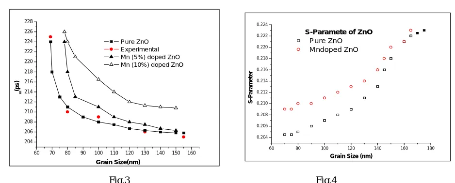
.60 70 80 90 100 110 120 130 140 150 160 204 206 208 210 212 214 216 218 220 222 224 226 228 Pure ZnO Experimental Mn (5%) doped ZnO Mn (10%) doped ZnO
m
(p
s
)
Grain Size(nm)
60 80 100 120 140 160 180
0.204 0.206 0.208 0.210 0.212 0.214 0.216 0.218 0.220 0.222 0.224
S-Paramete of ZnO
Pure ZnO Mndoped ZnO S -P a ra m e te r
[image:4.612.70.539.303.492.2]Grain Size (nm)
Fig.3 Fig.4
figure 3: comparison of calculated mean positron lifetime (
M ) as a function of grain size in pure zno thin films and mn doped zno thin films with the experimental observations of p.m.g. nambissan [14] for zns.figure 4: comparison of calculated S-parameter as a function of grain size in pure ZnO and Mn doped ZnO thin films.
If the diffusion length L+ competes the size of the grain the probability of the transition rate from free to grain boundary is high. Pasquini et al [13] have shown that the trapping coefficient for the thermal vacancy shows an increasing trend as temperature rises. Further, the trapping rate is expected to be proportional to the thermal vacancy concentration.
of the different positron trapping sites including the trapping into thermal vacancies inside the grains. Information regarding vacancy concentration in fine-grained samples in principle could be obtained from PAS data. In case of ZnO doping the size of the nanovoid cavity changes due to the increase in doping concentration. The free volume hole concentration has been found to decrease with the increase in doping concentration. Thus positron annihilation is a powerful tool for defect studies on a nanoscopic scale. It is applicable in almost all materials which are important in material science and is more suitable for study of bulk as well as near-surface properties of thin films.
REFERENCES [1] Wada K and Hyodo T 2013 J. Phys: Conf. Ser. 443 012003
[2] D.C. Look, Mat. Sci. Eng. B, 80, 383, (2001).
[3] N. Katsarakis, M. Bender, V. Cimalla, E. Gagaoudakis, G. Kiriakidis, Sensor. Actuat. B, 96, 76, (2003). [4] J.B. Lee, H.J. Lee, S.H. Seo, J.S. Park, Thin Solid Films, 398/399 641, (2001).
[5] Djurisic AB, Leung YH 2;8/9:944–961 (2006) [6] Djurisic AB, Ng AMC, Chen XY, 34:191–259 (2010) [7] Janotti A, Van de Walle CG Rep Prog Phys 72:126501(2009)
[8] Brandt, W., Dupasquier, A.: Positron Solid State Physics. North Holland, Amsterdam (1983) [9] Dupasquier, A., Mills Jr., A.P.: Positron Spectroscopy of Solids. IOS, Amsterdam (1995)
[10] Krause-Rehberg, R., Leipner, H.S.: Positron Annihilation on Semiconductors—Defect Studies. Springer, Berlin (1999) [11] Ishii, A.: Positrons at Metallic Surfaces. Trans Tech, Aedermannsdorf (1992)
[12] R. Krause-Rehberg, H.S. Leipner „Positron Annihilation in Semiconductors“ Springer-Verlag, 1999 ISBN 3-540-64371-0 [13] L. Pasquini, A.A. Rempel, R. Wurschum, K. Reimann, M.A. Muller, B. Fultz, and H.E. Schaefer, Phys. Rev. B 63, 134114 (2001).