Technology (IJRASET)
D–STATCOM Based Multi-Level Inverter for
Reactive Power Compensation
Srinivasa Acharya1 , B. Trinadha2, B. Srinivasa Rao 3 1,2
Assistant professor, 3Associate professor
Dept. of EEE, Aditya Institute Of Technology And Management, Tekkali , Srikakulam (Dist),A.P, India
ABSTRACT-The line upgrading techniques with Static Synchronous Compensator (STATCOM) is one of the promising technologies applied to improve power system performance. The STATCOMs in the distribution utilities (DSTATCOMs) are increasingly investigated for dynamic reactive power compensation and power quality improvement in the distribution utilities. This paper presents an investigation of seven-Level Cascaded H - bridge (CHB) Inverter as Distribution Static Compensator (DSTATCOM) in Power System (PS) for compensation of reactive power and harmonics. The simplification and analyzing of three phase circuits can be done by d-q reference frame theory. The DST ATCOM helps to improve the power factor and eliminate the Total Harmonics Distortion (THD) drawn from a Non- Liner Diode Rectifier Load (NLDRL). Finally a level shifted PWM (LSPWM) and phase shifted PWM (PSPWM) techniques are adopted to investigate the performance of CHB Inverter. The results are obtained through Matlab / Simulink software package.
Keywords: DSTATCOM, Cascaded H bridge (CHB), proportional integral (PI) control, D-Q reference frame theory.
I. INTRODUCTION
Technology (IJRASET)
inverters are being widely used because of their modularity and simplicity. Various modulation methods can be applied to CRB inverters. CRB inverters can also increase the number of output voltage levels easily byincreasing the number of R-bridges. This paper presents a DSTATCOM with a proportional integral controller based CRB multilevel inverter for the harmonics and reactive power mitigation of the nonlinear loads. This type of arrangements have been widely used for PQ applications due to increase in the number of voltage levels, low switching losses, low electromagnetic compatibility for hybrid filters and higher order harmonic elimination.
A. Static Synchronous Compensator
[image:3.612.232.333.270.351.2]Static Synchronous Compensator (STATCOM) is a voltage source converter based FACTS controller. It is a shunt controller mainly used to regulate voltage by generating/absorbing reactive power. The schematic diagram of STATCOM is shown in Fig. 1. STATCOM has no long term energy support in the DC Side and cannot exchange real power with the ac system ; however it can exchange reactive power. The reactive power is varied by varying the magnitude of the converter output voltage. A small phase difference exists between the converter output voltage and STATCOM bus voltage so that real power is drawn from the lines to compensate for the losses. STATCOMs are employed at distribution and transmission levels – though for different purposes.
Fig.1. schematic diagram of STATCOM
B. Voltage Source Converters
In recent years, voltage source converter technology has made a great progress through the development of high power self-turnoff type semiconductor devices. The rating for converter of this type in practical application has already reached as high.
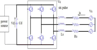
Because of its advantage over the line commutated type in performance characteristics and compactness, various applications of the voltage source converter have been developed and researched.Three phase Voltage Source Converter (VSC) is heart of most new FACTS and custom power equipments. It may be employed as a series or shunt element or combination of both, as in case of Unified Power Flow Controller (UPFC). Multilevel Voltage Source Converter topology is superior alternative to multipulse arrangement for high power applications like STATCOM. Voltage source converters (VSC) are commonly used to transfer power between a dc system and an ac system or back to back connection for ac systems with different frequencies, such as variable speed wind turbine systems[2]. A basic VSC structure is shown in Fig. 2 where Rs and Ls represent the resistance and inductance between the converter ac voltage (VC) and the ac system voltage (Vs) and Is is the current injected into the grid. A dc capacitor is connected on the dc side to produce a smooth dc voltage. The switches in the circuit represent controllable semiconductors, such as IGBT or power transistors. 6-pulse D-STATCOM configuration with the IGBT’s used as power devices. The IGBTs are connected anti parallel with diodes for commutation purposes and charging of the DC capacitor .For converter the most important part is the sequences of operation of the IGBTs. The IGBTs signals are referred to the Pulse Width Modulation (PWM) that will generate the pulses for the firing of the IGBTs. IGBTs are used in this simulation because it is easy to control the switch on and off of their gates and suitable for the D-STATCOM.
[image:3.612.223.389.616.702.2]Technology (IJRASET)
C. Basic Configuration and Operation Of DSTATCOM
When a STATCOM is employed at the distribution level or at the load end for power factor improvement and voltage regulation alone it is called D-STATCOM. Fig.2 shows a basic configuration diagram of the D-STATCOM. The D-STATCOM mainly consists of DC voltage source behind self-commutated inverters using IGBT and coupling transformer. The IGBT inverter with a DC voltage source can be modeled as a variable voltage source. The distribution power system can also be modeled as a voltage source. Two voltage sources are connected by a
I=(V-V0)/X (1)
[image:4.612.180.414.269.419.2]Reactor representing the leakage reactance of the transformer. The principle operation modes of the D-STATCOM output current, I which varies depending upon the voltage.Where V, Vo, X are the system voltage, output voltage of the IGBT-based inverter, the total ckt reactance respectively. If is equal to V, then no reactive power is delivered to the system. If is greater than V, the phase angle of I is leading with respect to the phase angle of V by 90 degrees. Thus, a leading reactive power flows in the Capacitive Mode of the D-STATCOM. If is lower than V, the phase angle of I is lagging with respect to the phase angle of V by 90 degrees. Thus, a lagging reactive power flows in the Inductive Mode of the D-STATCOM.
Fig.3.Single-line diagram of D-STATCOM
II. H-BRIDGE MULTILEVEL INVERTER
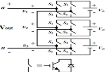
The traditional two or three levels inverter does not completely eliminate the unwanted harmonics in the output waveform. Therefore, using the multilevel inverter as an alternative to traditional PWM inverters is investigated. In this topology the number of phase voltage levels at the converter terminals is 2N+1, where N is the number of cells or dc link voltages. In this topology, each cell has separate dc link capacitor and the voltage across the capacitor might differ among the cells. So, each power circuit needs just one dc voltage source. The number of dc link capacitors is proportional to the number of phase voltage levels .Each H-bridge cell may have positive, negative or zero voltage. Final output voltage is the sum of all H-bridge cell voltages and is symmetric with respect to neutral point, so the number of voltage levels is odd. Cascaded H-bridge multilevel inverters typically use IGBT switches. These switches have low block voltage and high switching frequency.Fig.4.
[image:4.612.199.376.576.696.2]Technology (IJRASET)
Consider the seven level inverter; it requires 12 IGBT switches and three dc sources. The power circuit of inverter is shown in the figure 4. A cascaded H-bridges multilevel inverter is simply a series connection of multiple Hbridge inverters. Each H-bridge inverter has the same configuration as a typical single-phase full-bridge inverter.
[image:5.612.203.448.167.286.2]The cascaded H-bridges multilevel inverter introduces the idea of using Separate DC Sources (SDCSs) to produce an AC voltage waveform. Each H-bridge inverter is connected to its own DC source Vdc. By cascading the AC outputs of each H-bridge inverter, an AC voltage waveform is produced.
Fig 5. Output Voltage of cascaded H-bridge seven level inverter
By closing the appropriate switches, each H-bridge inverter can produce three different voltages: +Vdc, 0 and -Vdc. It is also possible to modularize circuit layout and packaging because each level has the same structure, and there are no extra clamping diodes or voltage balancing capacitors. The number of switches is reduced using the new topology. This circuit is simulated using the MATLAB software. The results are shown in the later sections in detail.
III. PROPOSED TOPOLOGY
[image:5.612.189.406.431.575.2]The main objective is to improve the quality output voltage of the multilevel inverter with reduced number of switches. An important
Fig.6. Proposed Power circuit for 7-level output
issue in multilevel inverter design is that to generate nearly sinusoidal output voltage waveform and to eliminate lower order harmonics. A key concern in the fundamental switching scheme is to determine the switching angles in order to produce the voltage with fundamental frequency. There are three modes of operation for the proposed 7-level multilevel inverter. These modes are explained as below.
A. Powering Mode
Technology (IJRASET)
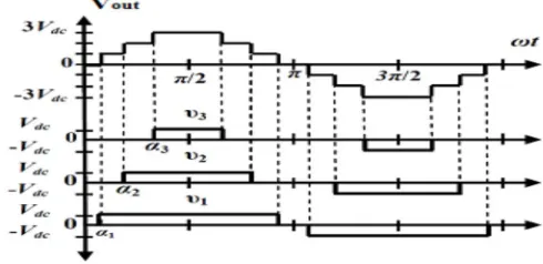
2Vdc, current pass is; the lower source, Q5, the upper source, Q1, load, Q4, and back to the lower source. When the output voltage is 3Vdc, the current pass comprises: upper supply, Q1, load, Q4, Q7, lower supply. In the negative half cycle, Q1 and Q4 are replaced by Q2 and Q3 respectively.
Fig.7. Waveforms of the proposed seven level inverter
B. Free-Wheeling Mode
Free-wheeling modes exist when one of the main switches is turned-off while the load current needs to continue its pass due to load inductance. This is achieved with the help of the anti-parallel diodes of the switches, and the load circuit is disconnected from the source terminals. In this mode, the positive half cycle current pass comprises; Q1, load, and D2 or Q4, load, and D3, while in the negative half cycle the current pass includes Q3, load, and D4 or Q2, load, and D1.
C. Regenerating Mode
In this mode, part of the energy stored in the load inductance is returned back to the source. This happens during the intervals when the load current is negative during the positive half cycle and viceversa, where the output voltage is zero. The positive current pass comprises; load, D2, Q6, the lower source, and D3, while the negative current pass comprises; load, D1, Q6, the lower source, and D4.
From the figure 7 switching pattern for the various switches are explained. In this paper fundamental frequency switching scheme is employed which reduces the switching losses. Because the switching frequency is less in this method when compared to the other methods. Switching losses are directly proportional to the switching frequency.
IV. DESIGN OF SINGLE H-BRIDGE CELL A. Device Current
The IGBT and DIODE currents can be obtained from the load current by multiplying with the corresponding duty cycles. Duty
cycle, d = ½ (l +Kmsinwt) Where, m = modulation index K = + 1 for IGBT, -1 for Diode. For a load current given by
idevice=
2
I sin (wt-
) (2)The average value of the device current over a cycle is calculated as
idevice=
2
I
sin(
wt
-
)
x
(1
+
km
sinwt)dwt
2
=
2I
cos
Φ
g
K
2
Π
1
m(3)
The device RMS current can be written as
i
rms
=
Technology (IJRASET)
=
cos
Φ
3
Π
K
g
1
I
2
m
(4)B. IGBT Loss Calculation
IGBT loss can be calculated by the sum of switching loss and conduction loss. The conduction loss can be calculated by,
Pon(IGBT) =
V
ceo
* Iavg(igbt)+ I2 rms(igbt)* rceo (5)Iavg(igbt) =
2
I
cos
Φ
g
m
2
Π
1
(6)
Irms(igbt)=
2
I
cos
Φ
3
Π
m
g
1
(7)
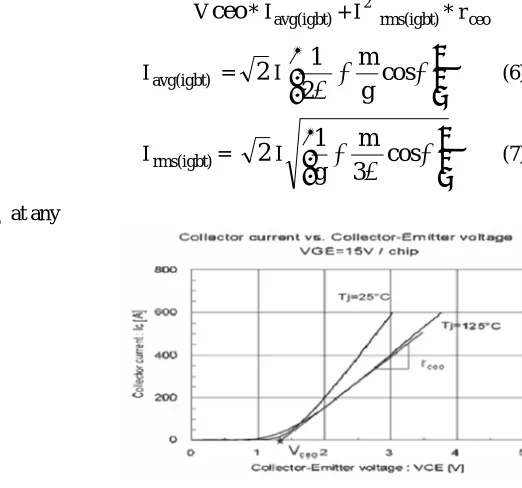
Values of Vceo and rceo at any
[image:7.612.139.400.187.431.2]junction
Fig. 8 IGBT output characteristics
temperature can be obtained from the output characteristics (Ic vs. Vce) of the IGBT as shown in Figure-8.
The switching losses are the sum of all turn-on and turn-off energies at the switching events
Esw= Eon+ Eoff = a+ bI + cI2 (8)
Here VDC is the actual DC-Link voltage and Vnom is the DC Link Voltage at which Esw is given. Switching losses are calculated
by summing up the switching energies
Psw=
E
(i)
T
1
sw n 0
(9)Here 'n' depends on the switching frequency
Psw = n
0
T
1
a
+
bI
+
cI
2
= 0
T
1
4
cI
Π
bI
2
a
2 (10)Technology (IJRASET)
Psw(IGBT) = fsw
nor DC 2
V
V
*
4
cI
Π
bI
2
a
(11)So, the sum of conduction and switching losses is the total losses given by
PT(IGBT) = Pon(IGBT)+ Psw(IGBT) (12)
C. Diode Loss Calculation
The DIODE switching losses consist of its reverse recovery losses; the turn-on losses are negligible.
Erec=
a
+
bI
+
cI
2 (13)Psw(DIODE) = Pon(DIODE) + Psw(DIODE) (14)
So, the sum of conduction and switching losses gives the total DIODE looses.
PT(DIODE) = P
on(DIODE) + Psw(DIODE) (15)
The total loss per one switch (IGBT +DIODE) is the sum of one IGBT and DIODE loss.
PT = PT(IGBT)+ Psw(DIODE) (16)
D. Thermal Calculations
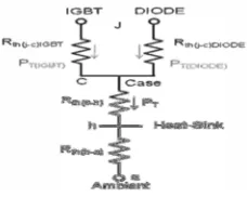
The junction temperatures of the IGBT and DIODE are calculated based on the device power losses and thermal resistances. The thermal resistance equivalent circuit for a module is shown in Fig 5. In this design the thermal calculations are started with heat sink temperature as the reference temperature. So, the case temperature from the model can be written as follows.
TC= PTRth(ch)+ Th (17)
Here Rth(ch)= Thermal resistance between case and heatsink
PT= Total Power Loss (IGBT + DIODE) (18)
IGBT junction temperature is the sum of the casetemperature and temperature raise due to the power losses inthe IGBT.
Tj(DIODE) = PT(DIODE)+ Rth(jc)DIODE+ TC(19)
[image:8.612.249.363.513.604.2]The above calculations are done based on the average powerlosses computed over a cycle. So, the corresponding thermalcalculation gives the average junction temperature. In orderto make the calculated values close to the actual
Fig. 9 Thermal resistance equivalent circuit
values, transient temperature values are to be added to the average junction temperatures.
E. DC-Capacitor Selection
Technology (IJRASET)
Fig.10 H-Bridge converter
Ic= -
U
*
K
I
sin
2wt
2
1
V
1
WL ac dc
(20)Since the value of 'L' is very small, the above equation canbe simplified to
IC= -
U
*
K
sin
2wt
2
1
V
1
ac dc (21)IC= -K
wt
V
U
dc ac2
sin
*
2
1
= -K2
m
sin
2wt
(22)Here 'm' is the modulation index and
Icp= C
dt
du
pp; sin
2wt
=
2
m
I
2
= C2w*ΔVV
dc (23)C =
2
I
V
*
ΔV
1
4w
m
dc (24)F. PWM Techniques For CHB Inverter
The most popular PWM techniques for CHB inverterare 1. Phase Shifted Carrier PWM (PSCPWM), 2. LevelShifted Carrier PWM (LSCPWM).
1) Phase Shifted Carrier PWM (PSCPWM):
Fig.11 Phase Shifted Carrier PWM
Technology (IJRASET)
carrier phase shift of 1800/ m (No. of levels) for cascadedinverter 1S introduced across the cells togenerate the stepped multi level output waveformwith lower distortion.
2. Level Shifted Carrier PWM (LSCPWM): Figure-12shows the Level shifted carrierpulse width modulation. Each cell is modulatedindependently using sinusoidal unipolarwidth modulation and bipolar pulsewidthmodulation respectively, providing an even power distribution among the cells. A carrier Level shift by 1/m (No.
Fig.12 Level Shifted Carrier PWM
of levels) for cascaded inverter 1S introduced across the cells to generate the stepped multilevel output waveform with lower distortion.
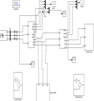
[image:10.612.233.376.165.306.2]IV. MATLAB/SIMULINK MODELING AND SIMULATION RESULTS
Figure- 13 shows the Matab/Simulink power circuit model of DSTATCOM. It consists of five blocks named as source block, non linear load block, control block, APF block and measurements block. The system parameters for simulation study are source voltage of llkv, 50 hz AC supply, DC bus capacitance 1550 e-6 F, Inverter series inductance 10 mH, Source resistance of 0.1 ohm and inductance of 0.9 mh. Load resistance and inductance are chosen as 30mh and 60 ohms respectively.
Fig. 13 Matlab/Simulink power circuit model of DSTATCOM
[image:10.612.232.389.436.604.2]Technology (IJRASET)
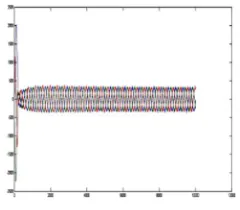
[image:11.612.236.358.239.349.2]Fig. 14seven level PSCPWM output
[image:11.612.244.364.376.481.2]Figure-15, 16, 17 shows the three phase source voltages, three phase source currents and load currents respectively without DST AT COM. It is clear that without DSTAT COM load current and source currents are same.
[image:11.612.242.369.517.650.2]Fig. 15 Three phase source voltage versus time
Fig. 16 Three phase source current versus time
Technology (IJRASET)
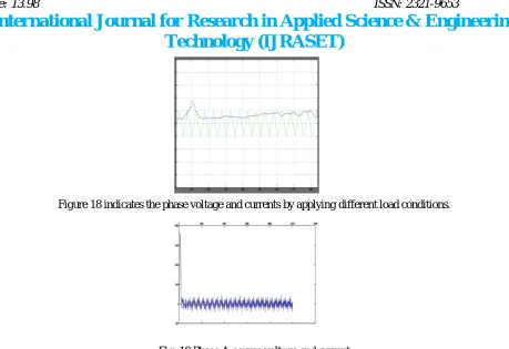
Figure 18 indicates the phase voltage and currents by applying different load conditions.
[image:12.612.233.363.81.204.2]Fig. 18 Phase A source voltage and current
Figure 19, 20 indicates controller fluctuations on both input and output sides. By using DSTATCOM the fluctuations are minimized in a less number.
Fig. 19 Controller input voltage fluctuations
Fig. 20 Controller output voltage fluctuations
Figure-21 shows the harmonic spectrum of Phase - A Source current without DST ATCOM. The THD of source current without DST ACOM is 31.31%.
Fig. 21 Harmonic spectrum of Phase-A Source current without DSTATCOM
[image:12.612.216.356.390.491.2] [image:12.612.244.369.569.678.2]Technology (IJRASET)
Fig. 21 Harmonic spectrum of Phase-A Source current with DSTATCOM
V. CONCLUSION
A DSTATCOM with seven levels CHB inverter is investigated. Mathematical modeling on multi-level inverters can be developed. The source voltage , loadvoltage , source current,load current, power factor simulation results under non-linear loads are presented. Finally Matlab/Simulink basedmodel is developed and simulation results are presented.
REFERENCES
[1] P.Bhagwat. and V.R.Stefanovic. "Generalized structure of a multilevel PWM Inverter:' IEEE Trans. Ind. Appln, VoI.IA-19. no.6, pp. I OS7-1069, Nov.!Dec .. 1983.
[2] J.Rodriguez. Jih-sheng Lai, and F Zheng peng, "Multilevel Inverters; A Survey of Topologies, Controls, and Applications," IEEE Trans. Ind. Electron., vol.49 , n04., pp.724-738. Aug.2002.
[3] Roozbeh Naderi, and Abdolreza rahmati, "Phase-shifted carrier PWM technique for general cascaded inverters," IEEE Trans. Power.Electron., vo1.23, no.3, pp. I 257-I 269. May.2008.
[4] Bhim Singh, Kamal AlHaddad & Ambrish Chandra, 1999, A Review of Active Filter for Power Quality Improvements, IEEE Trans on Industrial Electronics, 46(S), pp.960970
[5] Jason R. Wells, XinGengPatrick L. Chapman Philip T. Kreinand Brett M. Nee, “Modulation-Based Harmonic Elimination”, IEEE Transactions on power electronics, vol. 22, no. 1,pp336-340, 2007.
[6] J. Napoles, A. J. Watson, J. J. Padilla, J. I. Leon, L. G. Franquelo, P. W. Wheeler and M. A. Aguirre,”Selective Harmonic Mitigation Technique for Cascaded H-Bridge Converters with Non-Equal DC Link Voltages”, IEEE Transactions on power electronics,pp1-9,2012.
[7] John N. Chiasson, Leon M. Tolbert, Keith J. McKenzieand Zhong Du, “A Unified Approach to Solving the Harmonic Elimination Equations in Multilevel Converters”,IEEE Transactions on power electronics, vol. 19, no. 2, pp478-500,2004.
[8] A. Maheswari, S. Mahendran, Dr. I. Gnanambal, “Implementation of Fundamental Frequency Switching Scheme on Multi –Level Cascaded Hbridge Inverter Fed Three Phase Induction Motor Drive” Wulfenia journal,Klangfurt, Austria, Vol 19, No. 8, pp10-24,2012.
[9] S.J.Kim and S.K.Sul, “A novel filter design method for suppression of high voltage gradient in voltage-fed PWM inverter,” Proc. Appl. Power Electron. Conf.,1997, pp.122-127
[10] M.M.Swamy, K.Yamada, and T.Kume, “Common mode current attenuation techniques for use with PWM drives,” IEEE Trans. Power Electron., vol.16, pp.248-255, Mar. 2001
[11] S.Ogasawara, H.Ayano, and H.Akagi, “An active circuit for cancellation of common-mode voltage generated by a PWM inverter,” IEEE Trans. Power Electron. vol.13,pp.835-841, Sept.1998