Abstract—This paper presents the design and simulation of a High Efficiency DC/DC buck converter for mobile applications and systems on a chip (SOC) designed with CMOS technology 0.18 µm using SIMetrix and Cadence simulators. The circuit of the proposed buck converter was designed with both poly and 5 metals. First we compare the performance of the converter modes internal and external coil and the yield of sleep modes and bybass. Finally we present results of simulation of current and output voltages. The range of the supply voltage is [2,5V- 5.5V], the nominal switching frequency is 50MHz.
Index Terms— DC/DC Buck, High Efficiency, CMOS technology, Simetrix and Cadence Simulators.
I. INTRODUCTION
HIS section include the advantages, the characterization and the utilization of the DC-DC buck Converter. Power consumption has become one of the most important issues in modern electronics due to increased complexity and speed of the system. In order to curb the effect of power on a system as a whole, multiple power domains have been proposed as an architecture scheme for low power design. To support multi-Vdd, an array of supply voltages needs to be generated. DC/DC converters can be integrated on chip and convert the input voltage to different voltage levels in-ternally. The first method is convenient for relative low currents (few hundreds of mA) because the cost of an extra switch in the buck scheme limits the power efficiency. To miniaturize the DC-DC converter, the used strategy increases the operating frequency to reduce inductance and capacitance. Target is to obtain small values to enable on-chip or in-package integration, [1-4]. The request of currents below 1 A makes reasonable the sizes of power switches. The dynamic dissipation is relatively low and the operational frequency can be increased from nowadays 5 MHz to several tens or hundreds of MHz. However, high switching frequency causes a quadratic increase of power in
1Polydisciplinary Faculty of Ouarzazate, Department Mathematics and
Informatics and Management, Laboratory of Engineering Sciences and Energy, Ibn Zohr University- Agadir BP/638 Morocco, [email protected]
2Faculty of Sciences Department of Mathematic and Informatics,
Laboratory of Mathematic informatics and Applications Mohamed V University-Agdal Rabat BP/1014 Morocco, [email protected]
3,4Polydisciplinary Faculty of Ouarzazate, Laboratory of Engineering
Sciences and Energy, Ibn Zohr University- Agadir BP/638 Morocco, [email protected] , [email protected]
the control circuit that quickly becomes a non-negligible fraction of the dynamic dissipation, thus reducing efficiency. Buck converter aims at efficiencies higher than a linear regulator for a large range of the output current [5-25]. If the generated voltage Vout is D times the supply voltage, the efficiency of the linear regulator is D. Therefore, the goal is to keep system efficiency well above D for an extended range of output current. Just obtaining very high switching frequency [1, 2] is not practical. The goal of this design is to achieve for 1-A output current, efficiency higher than what reported in published research results, [3, 4].
This design reduces the power of the control loop at high switching frequency by a novel control strategy. Instead of using op-amps, the design employs current mode processing followed by a voltage-to-pulse converter. The total required current is as low as 45 µ A for switching frequencies up to 120 MHz. The buck converter, fabricated in a 0.18-µm CMOS technology with both poly and 5 metals, achieves 93% peak efficiency with 0.3A output current, 2.5-V output voltage, 50-MHz switching frequency and 5.5-V supply voltage. 22µF capacitor and requires clock and Vref/Vramp input of 1,23V.
II. DESIGNTOOLS A. Simetrix Smulator
The SIMetrix user interface provides an environment where multiple views can be managed within a window [26]. There are a range of views, for example content related views such as the Schematic Editor, Symbol Editor and Waveform Viewer, along with more system related views such as the Command Shell and File Viewer. By dragging a views title bar, views can be rearranged within a window into the layout that best suits the needs. We note that there are conceptually two types of views within SIMetrix. The first,System Views, provide tools to operate the program, which includes the Command Shell and File Viewer. The second,Workspace Views, provide means for developing and reviewing designs, which includes the Schematic Editor and Waveform Viewer.
Catena Software's SIMetrix/SIMPLIS is a popular Circuit Simulation package. SIMetrix/SIMPLIS is a combination ® of two independent circuit simulators: SIMetrix, a
SPICE-Designing and Simulation of High Efficiency
DC-DC Buck Converter Using the Tools
Simetrix and Cadence
1
Salah-ddine Krit, Member IAENG,
2Jalal Laassiri, Member IAENG,
3Kaoutar Bendaoud,
4Lahoucine
El maimouni
based simulator with numerous enhancements including custom models for power transistor devices; and SIMPLIS, a fast simulator that uses piecewise linear approximations and includes useful analysis modes for switching power supply circuits.
Circuit Simulation using SIMetrix and SIMPLIS in Altium Designer is similar to using Advanced Sim, Altium Designer's built-in simulator. Altium Designer supports SIMetrix/SIMPLIS in three main ways: Direct Simulation from Altium Designer using SIMetrix/SIMPLIS Using models from the SIMetrix/SIMPLIS model library, not only in the native SIMetrix and SIMPLIS simulators but in also in Altium Designer's built-in simulator Exporting Schematics containing simulation models to SIMetrix/SIMPLIS format.
B. Cadence Simulator
Analog Design Environment (ADE) is integrated on Cadence Custom IC Design software. The user can simulate his design (schematic, extracted layout, vhdl, etc.) using the ADE [27]. This tutorial explains necessary steps required in preparing your design and using ADE to simulate the circuit. The tutorial assumes that you have the inverter cell with schematic and symbol views created as described in “Virtuoso Schematic Composer Tutorial” (available on class website).
In the Cadence AMS simulator, compiled objects (modules, macromodules, and user-defined primitives) and other derived data are stored in libraries. The library structure uses a Library Cell: View approach, where:
A library relates to a specific design or to a reference library.
Cells relate to specific modules or building blocks of the design.
Views relate to different representations of the building blocks.
[image:2.595.310.549.49.271.2]III. PRINCIPLES OF PWMBUCK CONVERTERS This section covers the theoretical aspects of the DC-DC Buck converter. A practical method of designing the sliding coefficients is also introduced.
Fig. 1. Bsic Buck Converter Topology.
[image:2.595.65.276.576.720.2]This converter gives an output voltage vo smaller than the input voltage vs. It is based on the circuit of figure 1.
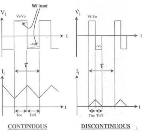
Fig. 2. Inductor voltage and inductor Current.
The figure 2 show the voltage and the current of the inductor in continuous and discontinuous mode.
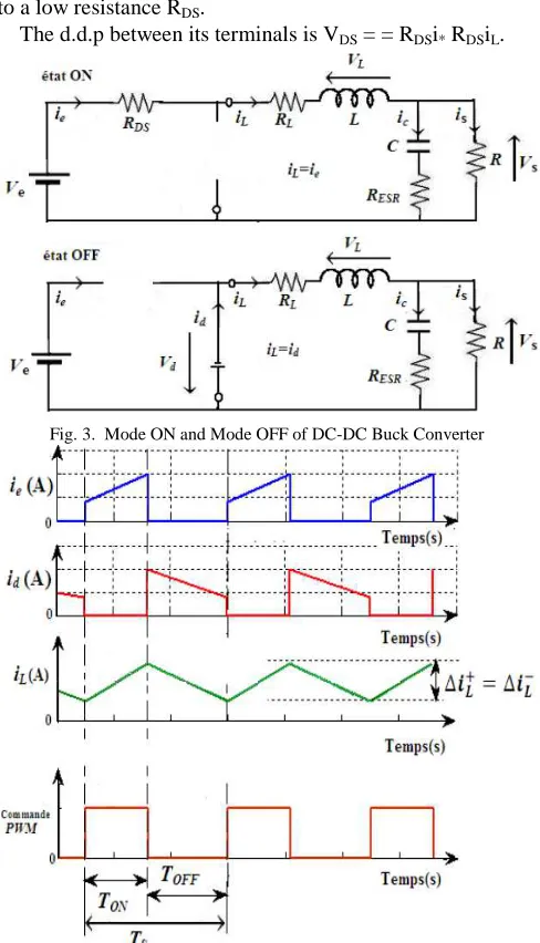
The operation of a buck converter can be divided into two time according to the state of Pch switch Fig.1 The ON state where the transistor Pch (Q) is on. The current through the inductance increases linearly. The voltage across the diode is negative, no current the crosses. The off-state when the transistor Pch (Q in the equations below) is blocked. The diode becomes conductive. it provides the continuity of the current in the inductor. The current through the inductor decreases.
The buck converter with ideal switching devices will be considered here which is operating with the switching period of T and duty cycle D, [1]. The state equations corresponding to the converter in continuous conduction mode (CCM) can be easily understood by applying Kirchhoff's voltage law on the loop containing the inductor and Kirchhoff's current law on the node with the capacitor branch connected to it. When the ideal switch is ON, the dynamics of the inductor current
i t
L( )
and the capacitorvoltage
v t
C( )
are given by,1
(
)
,
0
,
:
1
(
)
L
in o
o o
L
di
V
v
dt
L
t
dT
Q ON
dv
v
i
dt
C
R
=
−
< <
=
−
and when the switch is OFF are presented by,
1
( )
, , :
1
( )
L
o
o o
L
di
v
dt L dT t T Q OFF
dv v
i
dt C R
= −
< <
= −
A.CONDUCTION CONTINUE
to a low resistance RDS.
[image:3.595.48.292.53.479.2]The d.d.p between its terminals is VDS = = RDSi* RDSiL.
Fig. 3. Mode ON and Mode OFF of DC-DC Buck Converter
Fig. 4. Current and voltages obtained by continuous conduction of the buck converter
B.CONDUCTION DISCONTINUOUS
[image:3.595.312.546.54.305.2]In some cases, the amount of energy required by the load is low enough to be transferred in a shorter time than a switching period. During this part of the period the transistor M1 and the diode Da are blocked. [19] The current through the coil is canceled (IL = 0). The difference between the conduction and continuous conduction is added a third time (standby state) D3*Ts in the period Ts. The circuits of Fig.3 apply except that TOFF is different from (1 - D)*Ts. Fig.5 illustrates the variation with time of the current in the transistor ie, the current id in the diode, the current iL through the coil and the PWM voltage control of buck converter in discontinuous conduction mode.
Fig. 5. Current and voltages obtained by discontinuous conduction in a buck converter.
IV. SIMULATION RESULTS AND DISCUSSIONS
Experimental results show that, at the minimum 2.5V supply, the output control range is [0,5V- 2,45V] with an output current up to 0.3A.
Figure1 shows the yields depending on the load current of the converter internal mode (internal coil) and external mode (external coil). Figure 6 shows the yields depending on the load current of the converter to sleep mode (standby) and ON Mode (Bypass).
[image:3.595.308.548.561.758.2]The high voltage causes a greater dynamic dissipation This reduces the yield to low current. However low power control (only 35 µ A) holds the overall yield nearly a decade under the peak. Figure 7 and Figure 8 shows the currents and voltages across the components of the proposed buck converter, table 1 shows a comparison of the results of the proposed buck converter with references. The simulation results shows that the proposed converter is improved in performance for all modes compared the results.
Fig.5. Efficiency Versus the load current performance in internal mode and the external mode
Fig.6. Efficiency Versus the load current
[image:4.595.52.289.54.239.2]Fig.7. out voltage and output current of the proposed Buck Converter
Fig.8. Simulation results of the proposed DCDC Buck Converter . Efficiency Versus the load current
voltage and output current of the proposed Buck Converter
[image:4.595.48.288.518.722.2]e proposed DCDC Buck Converter
Table 1
Shows a comparison of the results of the proposed buck converter with references.
Reference Ve(min) Vs(min) Fs [17] 2,5 V 1,8 V 50
MHz
Proposed Buck
2,5 V 0,5 V 50 MHz
V. CONCLUSION This paper presented the design
buck Converter dedicated for mobile applications and systems on a chip (SOC) with CMOS technology 0.18 microns using SIMetrix and Cadence
achieved a new PWM circuit for controlling this model for different loads to optimize converter efficiency in ON mode (bypass) and sleep mode (standby). We compared the results of the converter output modes internal and external coil bobbin. This model was used of curre
loads. Against internal loop feedback between the output and the input of the power transistors ensures a switching voltage to zero in real time. This reduces the energy consumed by these transistors and achieves an efficiency of over 90% for a variety of charges. In addition, an external reaction against-loop is used in the PWM circuit to follow the new reference voltage.
REFERENCES
[1] J. Wibben and R. Harjani, “A High
Converter Using 2 nH Integrated Inductors”, IEEE Solid-State Circuits, vol. 43, pp. 844
[2] M. Wens and M. Steyaert, “A Fully
DC-DC Step-Down Converter, Regulated by a Constant On/Off-Time Control System”, Proc. of 2008 IEEE European Solid-State Circuits Conferenc
[3] P. Hazucha, G. Schrom, J. Hahn, B.A. Bloechel, P. Hack,G.E. Dermer, S. Narendra, D. Gardner, T. Karnik, V. De, and S.Borkar, “A 233-MHz 80%–
DC Converter Utilizing Air
IEEE J. of Solid-State Circuits, vol. 40, pp. 838 2005.
[4] K. Onizuka, K. Inagaki, H. Kawaguchi, M. Takamiya, and T. Sakurai, “Stacked-Chip Implementation of On
Converter for Distributed Power Supply System in SiPs”, IEEE J. Solid-State Circuits
2007.
[5] G J.S. Bridle, “Probabilistic Interpretation of Feedforward Classification Network Outputs, with Relationships to Statistical Pattern Recognition,” Neurocomputing Algorithms, Architectures and Applications, F. Fogelman Soulie and J. Herault, eds., NATO ASI
Springer-Verlag, pp. 227-236, 1989. (Book style with paper title and editor)
[6] Texas Instrument. "understanding buck power stages in switch mode power supplies". Mixed Signal Products, slva57, March 1999.
[7] J. Mahdavi, A. Emadi, and H. A. T
space averaging method to sliding mode control of PWM DC/DC converters,” in Proc.
a comparison of the results of the proposed buck converter with
Fs Technology efficiency 50
MHz
0,13 µm 2-poly 6-metal CMOS
76%
50 MHz
0,18 µm 2-poly 5-metal CMOS
90%
ONCLUSION
presented the design and simulations of a DC/DC onverter dedicated for mobile applications and systems on a chip (SOC) with CMOS technology 0.18 and Cadence simulators. We PWM circuit for controlling this model for different loads to optimize converter efficiency in ON mode (bypass) and sleep mode (standby). We compared the results of the converter output modes internal and external coil bobbin. This model was used of current values of different loads. Against internal loop feedback between the output and the input of the power transistors ensures a switching voltage to zero in real time. This reduces the energy consumed by these transistors and achieves an efficiency of ver 90% for a variety of charges. In addition, an external loop is used in the PWM circuit to follow
EFERENCES
J. Wibben and R. Harjani, “A High-Efficiency DC–DC Converter Using 2 nH Integrated Inductors”, IEEE J. of
State Circuits, vol. 43, pp. 844-854, April 2008. M. Wens and M. Steyaert, “A Fully-Integrated 130nm CMOS
Down Converter, Regulated by a Constant Time Control System”, Proc. of 2008 IEEE European State Circuits Conference, pp. 62-65, Sept. 2008. P. Hazucha, G. Schrom, J. Hahn, B.A. Bloechel, P. Hack,G.E. Dermer, S. Narendra, D. Gardner, T. Karnik, V. De, and –87% Efficient Four-Phase DC–
-Core Inductors on Package”, State Circuits, vol. 40, pp. 838-845, April
K. Onizuka, K. Inagaki, H. Kawaguchi, M. Takamiya, and T. Chip Implementation of On-Chip Buck Converter for Distributed Power Supply System in SiPs”, State Circuits, vol. 42, pp. 2404-2410, Nov.
J.S. Bridle, “Probabilistic Interpretation of Feedforward Classification Network Outputs, with Relationships to Statistical Pattern Recognition,” Neurocomputing— Algorithms, Architectures and Applications, F. Fogelman-Soulie and J. Herault, eds., NATO ASI Series F68, Berlin:
236, 1989. (Book style with paper
Texas Instrument. "understanding buck power stages in switch mode power supplies". Mixed Signal Products, slva57,
Conference, vol. 2, Oct. 1997, pp. 820-827.
[8] V. F. Pires, J. Fernando and A. Silva, “Teaching nonlinear modeling, simulation and control of electronic power converters using Matlab/SIMULINK,“ IEEE Transactions on Education, vol. 45, no. 3, pp. 301-315, August 2002.
[9] J. H. Su‚ J.J. Chen et D. S. Wu. "learning feedback controller design of switching converters via matlab/simulink". IEEE Transactions on Education, 45, 2002.
[10]D. Logue et P. T. Krein. "simulation of electric machinery and power electronics interfacing using matlab/simulink ". in 7th Workshop Computer in Power Electronics, 2000.
[11]A. Benlafkih‚ S. Krit et M. Chafik Elidrissi. "low voltage ,comparative study of pid controller and analog controller on dc/dc buck converter for mobile devices applications". International Conference on Information Systems and Technologies ICIST’13, TANGIE, MOROCCO. MARCH, 22 - 24, 2013.
[12]K. S. Leung et H. S. H. Chung. "a comparative study of the boundary control of buck converters using first- and secondorder switching surfaces -part i : Continuous conduction mode". IEEE PESC,pp. 2133–2139, 2005. [13]Venable Instruments. "optimum feedback amplifier design for
control systems".
[14]D. Mattingly. "designing stable compensation networks for single phase voltage mode buck regulators". Intersil Technical Brief TB417.1, 2003.
[15]Sipex société. "loop compensation of voltage-mode buck converters". 16, 2006.
[16]W. Keng. "switch-mode power converters, design and analysis". Academic Press, 2006.
[17]Youngkook Ahn, Hyunseok Nam, and Jeongjin Roh, Senior Member, IEEE "A 50-MHz Fully Integrated Low-Swing Buck Converter Using Packaging Inductors" IEEE TRANSACTIONS ON POWER ELECTRONICS, VOL. 27, NO. 10, OCTOBER 2012
[18]DCB Semiconductor. "5v, 2a, 1.5mhz step-down dc-dc converter". http ://www.bcdsemi.com, Rev. 1.0, 2012. [19]A. Benlafkih‚ S. Krit et M. Chafik Elidrissi. "design and
modeling of dc/ dc buck converterfor mobile device applications". Journées Doctorales en Technologies de l’Information et de la Communication "JDTIC’13", 29-30, Novembre ,kénitra-Maroc, 2013.
[20]M. Gildersleeve‚ H.P. Forghani zadeh et G.A. Rincon-Mora. "a comprehensive power analysis and a highly efficient, mode-hopping dc-dc converter". IEEE Asia-Pacific Conference on ASIC, pp. 153-156, 2002.
[21]J. Klein. "synchronous buck mosfet loss calculations with excel model". Fairchild Semiconductor Publication, 2006. [22]Yali Xiong‚ Shan Sun‚ Hongwei Jia‚ Patrick Shea et Z. John
Shen. "new physical insights on power mosfet switching losses". IEEE Transactions on Power Electronics, 24, 2009. [23]O. Djekic et M. Brkovic. "synchronous rectifiers vs. schottky
diodes in a buck topology for low voltage applications". Power Electronics Specialists Conference, 2, 1997.
[24]Sven E. Fagerstrom et Nagy N. Bengiamin. "buck/boost converter modeling and simulation for performance optimization". California State University at Fresno, Department of Electrical and Computer Engineering 5241 N. Maple Avenue, Fresno, CA 93740, U.S.A.
[25]F. Amatoul‚ M. Lamchich et A. Outzourhit. "design and simulation of dc/dc buck converter for stand alone photovoltaic energy system with lead acid battery storage". International journal of information scinces and Computer Engineering, 2, 2011.
[26]Simetrix Spice And Mixed Mode Simulation, Verilog-A LanguageReference Manual.www.simetrix.co.uk/Files/manual s/6.0/SimulatorReference.pdf