1
Electrical performance of conducting polymer (SPAN) grown on
GaAs with different substrate orientations
D A Jameela,b, M Aziza, J F Felixc,d, N Al Saqria,e, D Taylora, H Albalawia, H Alghamdia, F Al Masharya, M Heninia
aSchool of Physics and Astronomy, Nottingham Nanotechnology and Nanoscience Center University of Nottingham, NG7 2RD, United Kingdom
b
Department of Physics, Faculty of Science, University of Zakho, Kurdistan Region-Iraq cDepartamento de Física, Universidade Federal de Viçosa, 36570-900, Viçosa, Minas Gerais Brazil dUniversidade de Brasília, Instituto de Física, Núcleo de Física Aplicada, Brasília DF 70910-900, Brazil
e
Department of Physics, College of Science, Box 36, Sultan Qaboos University, Al Khoud, 123, Oman
This article reports the effect of n-type GaAs substrate orientation, namely (100),
(311)A and (311)B, on the electrical properties of sulfonated polyaniline (SPAN)/GaAs
heterojunction devices. In addition, the inhomogeneity of the interface between various
GaAs substrates and SPAN is investigated in terms of barrier height and ideality factor
by performing I-V measurements at different temperatures (20-420K). The I-V results
indicate that the value of the rectification ratio (IF/IR) at 0.5V is higher for SPAN/(311)B
GaAs samples than for SPAN/(100) GaAs and SPAN/(311)A GaAs samples. Moreover,
the barrier height decreases and the ideality factor increases with decreasing
temperature for all three heterostructure devices. The high value of mean barrier of
SPAN/(311)B (calculated from the plots of as a function of 1/2kT) confirms that the
GaAs substrate orientation results in an increase of barrier homogeneities. Furthermore,
the C-V characteristics were obtained at room temperature. The C-V measurements
showed that the carrier distributions at the interface and away from the interface in high
index (311) GaAs orientations are more uniform and have better barrier homogeneity
than those grown on the conventional (100) GaAs substrates.
Keywords
: (100) GaAs, (311)A GaAs, (311)B GaAs, I-V and C-V*Manuscript
2
1.
Introduction
Essentially conducting polymers, such as polyaniline (PANI), sulfonated polyaniline
(SPAN), poly(p-phenylene-vinylene), polypyrrole, polyacetylene, polythiophene, etc.,
are promising semiconductors materials with confirmed technological potential due to
their unique optical and electrical properties [1]. Among the family of organic
semiconductors, the semiconducting polymers have attracted the most attention for
applications in electronic and optoelectronic devices, particularly due to their
exceptional electrical properties and easy synthesis [2–4]. As a result, this category of
polymers has been used in several applications such as organic light emitting diodes
(OLEDs) [5,6], solar cells [7,8], battery electrodes [9,10], photodiodes [11], energy
storage [12], transistors [13], gas sensors [14], biosensors [15], radiation sensors [16],
anti-corrosive coatings [17,18] and electromagnetic interference shielding [19].
Sulfonated polyaniline (SPAN), which is particularly a p-type semiconductor,
represent a class of self-doped conducting polymers and a derivative of PANI, has
received a great interest in recent years, because of its unique electroactive physical
properties, enhanced process ability and potential industrial applications [20–22]. This
material is environmentally stable over a wide range of temperatures. It can be grown as
thin films over large areas at low cost [3]. In addition, SPAN has a big advantage in
electronic circuitry design [8] because it forms Ohmic contacts with metals used in
microelectronic applications such as Al, Ag and Cu. A typical band gap of SPAN is in
the range 2.755–2.883eV [23].
On the other hand, in recent years III–V compound semiconductors, and in
particular gallium arsenide (GaAs), have been used most frequently in the fabrication of
electronic and optoelectronic devices. Recently, high index GaAs substrates, such as
3
because the optical properties of heterostructures grown on (311)A GaAs and (311)B
GaAs are considerably better than those grown on (100) surfaces [24, 27].
As it is well known, the crystallographic orientation of the substrate has a significant
effect on incorporation of impurities and defects and consequently on optical and
electronic properties of III–V materials [28]. The ideality factor n and barrier height
(BH) as well as the electrical characteristics are fundamental parameters of a Schottky
barrier diode (SBD) and these give an indication about the quality of the Schottky
interface. The SBD parameters must be determined over a broad range of temperatures
because the analysis of the current-voltage (I-V) characteristics of the SBD measured
only at room temperature does not provide accurate information about the conduction
mechanism and the barrier nature created at metal semiconductor interface in order to
understand these phenomena and determine precisely the parameters of the Schottky
diodes. Chand et al.[29] and Hardikar et al.[30] analysed the experimental
current-voltage data which revealed that there is an increase in the ideality factor and a decrease
in the zero-bias barrier height with decreasing temperature. Consequently, the ideality
factor and the barrier height established from forward I-V characteristics are found to be
temperature dependent. This confirms that the Schottky barrier height is inhomogeneous
in nature at the interface. This behaviour has been successfully described on the basis of
the thermionic emission mechanism with Gaussian distribution of the barrier height
[31].
To fabricate a hybrid organic/inorganic semiconductor heterojunction device with
the aim to obtain specific optical and electrical properties on the bases of their doping
levels, a thin organic film is deposited onto the surface of a conventional inorganic
4
spin coating used for thin film deposition at room temperature. Recently, a new
technique of SPAN films preparation has been developed by Yang et al. [32].
In this paper, we report on the fabrication and electrical characterization of
Au/SPAN/GaAs heterojunctions grown on three different substrate orientations, namely
n-type GaAs (100), (311)A and (311)B. We have investigated the effect of the substrate
orientation on the heterojunction parameters such as barrier height and ideality factor as
a function of the temperature. Additionally, in order to understand the behaviour of the
devices barrier homogeneity Capacitance-Voltage (C-V) measurements were performed
at room temperature.
2.
Materials and Methods
2. 1. Devices fabrication
The n-type silicon-GaAs substrates with a concentration of 2x1018 cm−3 were used to
growth SPAN. The SPAN thin films have been grown on (100), (311)A and (311)B
GaAs substrates by self-assembly. For this, after the cleaning process of substrates, a
backside electrical contact of nickel (Ni)-gold (Au) was deposited by thermal
evaporation using a BOC Edwards 306 system. For more details see procedure
described elsewhere [13,33]. Subsequent to the backside electrical deposition, a 200 nm
thick SPAN thin film was deposited onto the (100), (311)A and (311)B GaAs epitaxial
layer at a rate of 1.8 nm/h by adopting a procedure based on the process initially
developed by Yang et al. [32] and described in Ref.[13], except that the aniline and
metanilic acid amounts (455 μl and 1.715 g, respectively) and the growth temperature
(10 °C) are different. Finally, a circular electrical contact was obtained by thermal
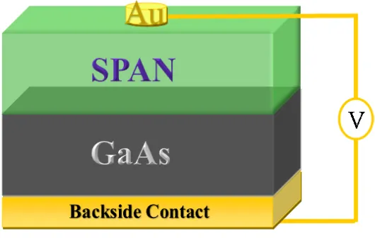
5
GaAs, SPAN/(311)A GaAs and for SPAN/(311)B GaAs hybrids devices, as shown
schematically in Fig. 1.
2. 2. Device characterization
The temperature dependence of the I-V characteristics in the temperature range of
20–420 K with intervals of 20K was measured by using a current source measurement
unit (Keithley 236) and a closed-loop helium cryostat (Janis CCS-450).
Capacitance-Frequency measurements were performed using LCR meter (Agilent E4980). The
thicknesses of the thin films were measured on a profilometer (Dektak 6M).
3.
Results and Discussion
3.1
. Current–Voltage Characteristics
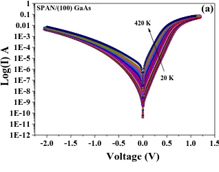
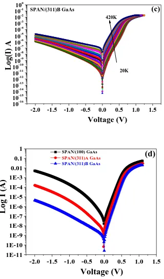
The electrical I-V measurements were performed in the temperature range of 20-420
K with a temperature step of 20 K on SPAN/(100) GaAs, SPAN/(311)A GaAs and
SPAN/(311)B GaAs samples to study the diode parameters such as the series resistance
(Rs), the ideality factor (n) and the barrier height (ϕBo). Typical forward and reverse bias
I-V characteristics of SPAN/(100) GaAs, SPAN/(311)A GaAs and SPAN/(311)B GaAs
n-type heterostructures in a semi-logarithmic scale are shown in Fig. 2(a–b),
respectively. Fig. 2(d) shows a semi-logarithmic I-V plots at room temperature of
SPAN/(100) GaAs, SPAN/(311)A GaAs and SPAN/(311)B GaAs. Clearly as illustrated
in Fig. 2(d), the SPAN/(311)B GaAs heterostructures exhibit better I–V characteristics
6
at room temperature and applied voltage of 0.5 V the value of the rectification ratio
(which is the ratio of forward current (IF) to the reverse current (IR)) is approximately
2x10², 3.7x10³ and 1.7x10⁴ for SPAN/(100) GaAs, SPAN/(311)A GaAs and
SPAN/(311)B GaAs samples, respectively. It is worth noting that the rectification value
is highest in samples grown on (311)B GaAs substrates. This is one of the indications
that the interface charges between SPAN and GaAs (311)B substrates are the lowest.
In order to explore further the electrical behaviour of the organic/inorganic
semiconductor devices parameters such as series resistance, barrier height and ideality
factor are extracted by modelling the devices as Schottky diodes. As can be seen from
Fig. 2(a, b and c), the forward bias I-V plots were not perfectly linear and displayed a
downward concave curvature at high voltage. This downward curvature originates from
the presence of a small series resistance (Rs) as determined from the analysis of the
experimental forward I-V characteristics. The obtained values of Rs ranged from 6.5–
8.25 Ω, 12–20.7 Ω and 8.7–11 Ω for SPAN/(100) GaAs, SPAN/(311)A GaAs and
SPAN/(311)B, respectively. The experimental current–voltage (I–V) data were
modelled by the well-known thermionic emission (TE) equation at forward bias (V ≥
3kT/q) [34].
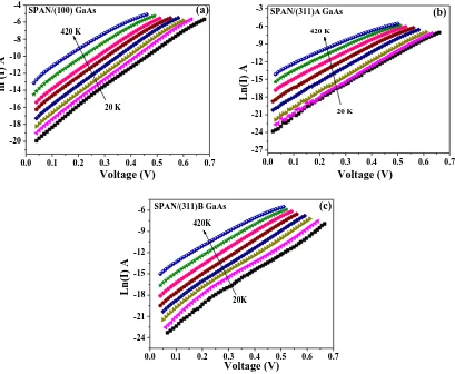
where is the saturation current determined by extrapolating the linear portion in the
ln(I) versus V plot (Fig. 3) to the intercept point on the current axis at V = 0 [35] and
defined by
7
In the above equations, q is the electronic charge, V is the forward-bias voltage, k is
the Boltzmann constant, T is the absolute temperature, is the zero-bias barrier
height, S is the effective diode area, and is the effective Richardson constant of 8.16
Acm-2k-2 for n-type GaAs [35]. From equation (1), the ideality factor ‘n’, which is a
dimensionless quantity, represents a measure of the conformity of the diode behaviour
to pure thermionic emission. n can be expressed as
According to the TE theory, the zero-bias BH and the ideality factor n, for all
three samples, are determined from intercepts and slopes of the forward-bias ln(I)
versus V plot at each temperature (Fig. 3), respectively. For SPAN/(100) GaAs
heterojunctions, the values of and n changed from 0.039 eV and 25.24 (at 20K) to
0.76 eV and 1.48 (at 420 K), respectively. Whereas, for SPAN/(311)A GaAs device,
these values change from 0.044 eV and 22.44 to 0.80 eV and 1.44, respectively, for the
same temperature range. While for SPAN/(311)B GaAs devices the obtained values of
and n varied from 0.053 eV and 19.4 to 0.86 eV and 1.4, respectively. The high
quality of the SPAN/n-GaAs devices is confirmed by the high values of and the low
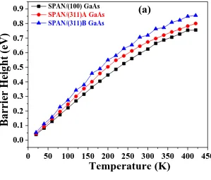
values of n (an ideal diode has an n of 1) at room temperature. It can be seen from Fig.
4(a) and (b) that the zero-bias barrier height and ideality factor reveal strong
temperature dependence, that is the value of decreases and n increases with the
decrease of temperature for all three devices. This behaviour was also observed in
8
across the organic/inorganic interface is a temperature activated process, where
electrons at low temperatures are able to overcome only the lower barriers and as a
result, the current transport will be dominated by the current flowing through the
regions of lower and larger n [1]. This means that more and more electrons have
sufficient energy to surmount a higher barrier when the temperature increases.
Subsequently, in addition to the regions of the heterojunction with low barrier heights,
the dominant barrier heights in other regions will increase with temperature and voltage
bias [35, 36]. Furthermore, an apparent decrease in BH and increase in ideality factor at
low temperatures are due to the barrier inhomogeneity and other effects such as defects,
thickness inhomogeneity and non-uniformity of the interfacial charges [30].
The zero-bias barrier height at room temperature, as seen in Fig. 4(a) is calculated to
be 0.62 eV, 0.67 eV and 0.72 eV for the SPAN/(100) GaAs, SPAN/(311)A GaAs and
SPAN/(311)B GaAs heterostructures, respectively. of SPAN grown on (311)B
GaAs substrate is greater than that of SPAN grown on (100) and (311)A GaAs
substrates. This value is also greater than the value reported by Felix et al. [37] for
SPAN/4H-SiC hybrid devices. In addition, the ideality factor at room temperature is
determined to be 1.77 for the SPAN/(100) GaAs, 1.63 for SPAN/(311)A GaAs and 1.61
for SPAN/(311)B GaAs devices, as shown in Fig. 4(b). Taking into account the fact that
n = 1 for an ideal diode, it is observed that n values differ from unity for all the three
devices, however the SPAN/(311)B GaAs device is nearest to the ideal case. When the
experimental values of n are higher than unity, thisdeviation from unity is attributed to
the bias dependence of the barrier height and barrier inhomogeneity. The high values of
the ideality factor are also probably due to a potential drop in the interfacial layer and
the presence of excess current as well as the recombination current through the
9
worth pointing out that the higher barrier height and lower ideality factor values for
SPAN/(311)B GaAs devices is an evidence of their excellent electrical properties and
good homogeneities when compared with SPAN grown on (100) and (311)A GaAs
heterojunctions. It is important to note that the electrical properties and barrier
homogeneities of SPAN grown on (311)A plane are better than those of sample grown
on (100) orientation. Therefore, the substrate orientation has a strong impact on the
electrical properties and barrier inhomogeneities of the devices.
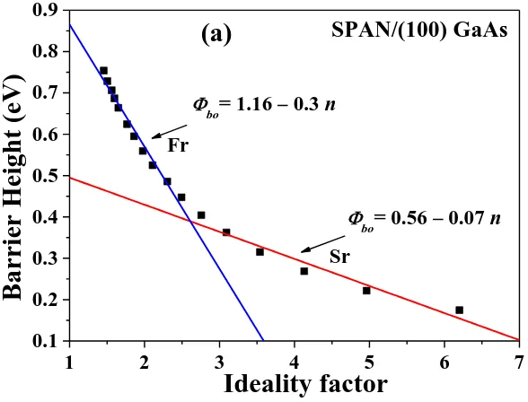
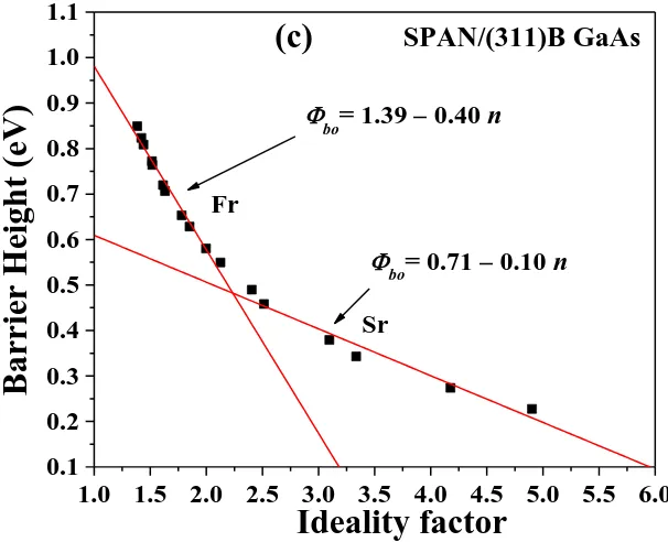
Fig. 5(a – c), show the variation of as a function of n for the SPAN/(100) GaAs,
SPAN/(311)A GaAs and SPAN/(311)B GaAs heterojunctions, respectively. According
to these figures, the barrier height is correlated linearly with the ideality factor with an
extrapolated at n = 1 that would correspond to the laterally homogeneous barrier
height and for which pure TE applies as the unique mechanism through which
conduction takes place. Note that the versus n characteristics for the three devices
show two linear regions, namely first region (Fr) and second region (Sr), over two
temperature ranges (420-200K) and (180-40K), respectively, with two extrapolated
barrier heights at n = 1. For SPAN/(100) GaAs hybrid devices (Fig. 5(a)), the value of
at n = 1 of Fr and Sr regions is 0.86 eV and 0.49 eV, respectively. While for
SPAN/(311)A GaAs devices, the value of at n = 1 of the Fr region is 0.94 eV and
of the Sr region is 0.55 eV, as shown in Fig. 5(b). However, for SPAN/(311)B GaAs
devices, these values are 0.99 eV and 0.61 eV for the same regions, as shown in Fig.
5(c).
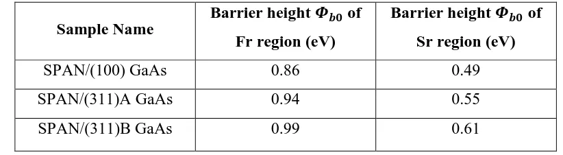
The value of barrier height at n = 1 of Fr and Sr regions for the three devices are
presented in Table 1, where one can observe that the value of Fr region and Sr
region increase as the substrate orientation n-GaAs is changed from (100) to (311)A and
10
significant role in improving the electrical properties and barrier homogeneity of the
devices. Sellai et al. [39] pointed out that the barrier height found by extrapolation to n
= 1 may be considered as a reasonable good estimate for the homogeneous barrier
height. Thus, the barrier of SPAN/(311)B GaAs samples is more homogeneous, because
value at n = 1 for both regions are higher than those of (100) GaAs and (311)A
GaAs samples.
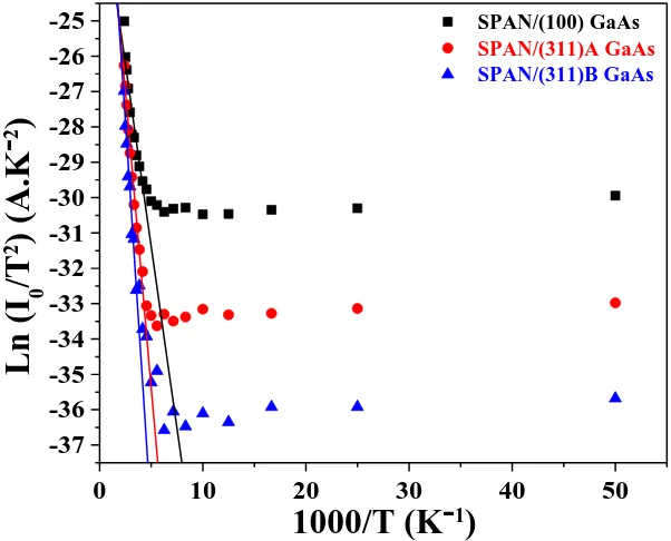
The barrier height can also be determined by rewriting equation (3) (see equation 5)
and using the Richardson plot of the saturation current
The plots of ln(Io/T2) versus 1000/T for SPAN/(100) GaAs, SPAN/(311)A GaAs
and SPAN/(311)B GaAs heterojunctions are depicted in Fig. 6. The experimental data
are seen to fit well with a straight line over a wide range of temperatures. According to
equation (5), the plot of ln(Io/T2) versus 1000/T yields the zero-bias barrier height
from the slope and the Richardson constant from the intercept of the straight line. The
zero-bias barrier height values as obtained from the slope of the straight lines
portion of the curves for SPAN/(100) GaAs, SPAN/(311)A GaAs and SPAN/(311)B
GaAs devices are 0.18 eV, 0.29 eV and 0.38 eV, respectively. The higher barrier energy
value for SPAN/(311)B GaAs devices could be indicative of less traps and defects, and
therefore better electrical properties and homogeneity, when compared with SPAN
grown on (100) and (311)A GaAs substrates. On the other hand, the value of
Richardson constants obtained from the intercept of the straight lines portion of the
curves and are 3.53×10⁻⁷ Acm-2K-2, 3.75×10⁻⁶ Acm-2K-2 and 1.2×10⁻⁵ Acm-2K-2 for
11
respectively. These values are much lower than the well-established value of 8.16 Acm
-2
K-2 for n-type GaAs. These deviations from the known Richardson constant may be
due to the spatial inhomogeneous barrier and potential fluctuations at the interface that
consist of low and high barrier areas. Moreover, nonlinear behaviour of ln(Io/T2) as a
function of 1000/T plot at low temperatures is as a consequence of the extra current
contribution arising from the reduction in the barrier height [29, 40]. Although the
Richardson constant values for the three devices differ from the expected Richardson
value, SPAN/(311)B GaAs devices have the closest values. Consequently, it is worth
pointing out that the samples grown on (311)B GaAs substrates are more homogeneous
than samples grown on (100) and (311)A substrates.
The decrease in the ideality factor and the increase in barrier height with the
increase of temperature can also be explained on the basis of a thermionic mechanism
with Gaussian distribution of barrier heights due to the barrier height inhomogeneities
prevailing at organic/inorganic semiconductor interface [41]. In other words the
increase of the value of n with decrease of temperature is direct result of the bias
dependence of the mean barrier and the standard deviation of the Gaussian
distribution of barrier heights in Schottky diodes. The Gaussian distribution of the
barrier heights and variation of the ideality factor with temperature are expressed by the
following equations[41,42].
and
It is assumed that both the mean barrier at a given voltage ( ) as well as are
12
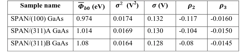
and [43], where , and n are mean barrier height, standard
deviation of the barrier height distribution and the ideality factor, respectively. Usually
the temperature dependence of is small and can be neglected. The coefficients and
are the voltage deformation of the barrier height distribution. The plots of as a
function of 1/2kT and (n-1-1) as a function of 1/2kT are shown in Fig. 7(a–c) for the
SPAN/(100) GaAs, SPAN/(311)A GaAs and SPAN/(311)B GaAs heterojunctions,
respectively. The plot of versus 1/2kT (Fig. 7(a), for SPAN/(100) GaAs) should be
a straight line that gives = 0.974 eV from the intercept and = 0.132 V from the
slope. In contrast, for SPAN/(311)A GaAs (see Fig. 7(b)) and SPAN/(311)B GaAs (see
Fig. 7(c)), the values of increased to 1.014 eV and 1.08 eV, respectively. However,
is reduced to 0.130 V for SPAN/(311)A GaAs and 0.128 V for SPAN/(311)B GaAs.
It is important to point out that the value of is not small compared to value for all
the three samples, confirming the presence of the interface inhomogeneties [42]. These
values are displayed in Table 2. S. Chand and J. Kumar [42] argued that the decrease of
the standard deviation leads to an increase in the barrier height and a decrease in the
ideality factor. The standard deviation is a measure of the barrier homogeneity. The
lower value of corresponds to a more homogeneous barrier height. Accordingly, the
SPAN/(311)B GaAs devices have better homogeneity and excellent electrical properties
when compared with SPAN grown on (100) and (311)A GaAs. The plot of (n-1-1)
versus 1/2kT as illustrated in Fig. 7(a–c) is a straight line that gives the voltage
coefficients and from the intercept and slope of the plot as = -0.117 and =
-0.0160 for the SPAN/(100) GaAs hybrid devices (Fig. 7(a)), while these coefficients are
changed to -0.104 and -0.0150, respectively, for the SPAN/(311)A GaAs hybrid devices
(Fig. 7(b)). Whereas, for SPAN/(311)B GaAs hybrid devices (Fig. 7(c)), the values of
13
illustrated in Table 2. From this table it can be seen that the value of , (- ) and (- )
is decreased by changing the substrate orientation n- GaAs from (100) to (311)A and
(311)B GaAs. Boyarbay et al.[41] investigated the electrical properties of the
Au/PANI/p-Si/Al and Au/PANI TiO2 TTAB/p-Si/Al heterojunctions. They reported
that the value of mean barrier decreases due to < 0 and the value of
decreases with decreasing (- . The same behaviour has been observed in this study,
thus, the value of increases as the substrate orientation is changed from (100) to
(311)A and (311)B GaAs. It means that of sample grown on (311)B substrate is
greater than that of (100) and (311)A. However, value of the SPAN/(311)B GaAs
sample decreased with decreasing (- ) leading to an increase in barrier height. This
confirms that the SPAN/(311)B samples have better barrier homogeneity and electrical
properties than the other two samples.
3.2
. Capacitance–Voltage Characteristics
In order to investigate further the barrier height homogeneity of the three samples,
the capacitance (C) as a function of voltage measurements were performed at room
temperature (300K). The C-V characteristics for the three devices demonstrate that the
capacitance increases as the reverse voltage tends to zero, as presented in Fig. 8. On the
other hand, as seen in Fig. 9(a), the 1/C2 versus V characteristics of the SPAN/(100)
GaAs is not linear indicating that the doping (concentration of carriers as a function of
depletion width) in the bias range -1.5V to 0V is neither uniform nor linearly graded
[43]. These results infer non-uniformity in the carrier distribution at the interface and
away from the interface. These effects could cause a non-homogeneous or a spatially
14
represented as 1/C2 versus V plots for the SPAN/(311)A GaAs and SPAN/(311)B GaAs
diodes (Fig. 9(b) and (c)) reveal approximately a linear behaviour which indicates that
the doping is uniform in the same bias range (depletion region). As a result, the carrier
distribution at the interface and away from interface is uniform and consequently the
barrier height could be more homogeneous for SPAN grown on (311) GaAs
orientations.
4.
Conclusion
Organic semiconducting polymer SPAN grown on (100), (311)A and (311)B GaAs
substrates have been investigated. The current-voltage characteristics of the three
samples show that the value of the rectification ratio (IF/IR) at 0.5V is higher for
SPAN/(311)B GaAs samples than for SPAN/(100) GaAs and SPAN/(311)A samples.
Furthermore, a lower and higher n values in the sample grown on (100) and (311)A
GaAs could be attributed to more barrier inhomogeneity and other effects such as
defects and non-uniformity of the interfacial charges than in the samples grown on the
(311)B GaAs. The high values of Richardson constant and mean barrier also
confirm that the GaAs substrate orientation results in an increase of barrier
homogeneities. This is also supported by the higher value of and smaller value of
observed in the SPAN/(311)B GaAs samples. The value of increases due to
(-and decrease with decreasing (- . Moreover, the C-V measurements provide
evidence that the carrier distributions at the interface and away from the interface in
high index (311) GaAs orientation are more uniform and have better barrier
homogeneity than those of samples grown on the conventional (100) GaAs substrates.
15
substrate orientations of GaAs have also shown that the high index planes play a role in
improving the electrical properties of the samples. However, it is clear from this work
that the barrier homogeneity and electrical properties of the sample grown on the (100)
GaAs are not as good as those of the SPAN samples grown on the high index (311)
GaAs and particularly SPAN/(311)B GaAs.
Acknowledgement
The author would like to thank the Ministry of Higher Education of Kurdistan-Iraq
and University of Zakho for supporting his PhD studies at University of Nottingham,
UK. Also the authors would like to thank the Brazilian funding agencies through grants
from CAPES, FAPDF and CNPq for supporting this project under research grant
16
REFERENCES
[1] S.E. El-zohary, M.A. Shenashen, N.K. Allam, T. Okamoto, M. Haraguchi,
Electrical Characterization of Nanopolyaniline / Porous Silicon Heterojunction at High Temperatures, J. Nanomater. 2013 (2013) 1–8.
[2] S.-Y. Lee, G.-R. Choi, H. Lim, K.-M. Lee, S.-K. Lee, Electronic transport
characteristics of electrolyte-gated conducting polyaniline nanowire field-effect transistors, Appl. Phys. Lett. 95 (2009) 013113. doi:10.1063/1.3176444.
[3] X. Wei, Y.Z. Wang, S.M. Long, C. Bobeczko, A.J. Epstein, Synthesis and
Physical Properties of Highly Sulfonated Polyaniline, J. AM. Chem. Soc. 118 (1996) 2545–2555.
[4] F. Yakuphanoglu, E. Basaran, Electrical and Optical Properties of an Organic
Semiconductor Based on Polyaniline Prepared by Emulsion Polymerization and Fabrication of Ag / Polyaniline / n-Si Schottky Diode, J. Phys. Chem. B. 110 (2006) 16908–16913.
[5] S.E. Jang, J.Y. Lee, High power efficiency in single layer blue phosphorescent
organic light-emitting diodes, J. Lumin. 131 (2011) 2788–2791. doi:10.1016/j.jlumin.2011.07.014.
[6] T. Schwab, M. Thomschke, S. Hofmann, M. Furno, K. Leo, B. Lüssem,
Efficiency enhancement of top-emitting organic light-emitting diodes using conversion dyes, J. Appl. Phys. 110 (2011) 083118. doi:10.1063/1.3656452.
[7] J.A. Chang, J.H. Rhee, S.H. Im, Y.H. Lee, H. Kim, S. Il Seok, et al.,
High-performance nanostructured inorganic-organic heterojunction solar cells., Nano Lett. 10 (2010) 2609–12. doi:10.1021/nl101322h.
[8] R. Valaski, F. Muchenski, R.M.Q. Mello, L. Micaroni, L.S. Roman, I. a.
Hümmelgen, Sulfonated polyaniline/poly(3-methylthiophene)-based photovoltaic devices., J. Solid State Electrochem. 10 (2005) 24–27. doi:10.1007/s10008-005-0648-8.
[9] A.G. Macdiarmid, S.-L. Mu, N.L.D. Somasiri, W. Wu, Electrochemical
17
Mol. Cryst. Liq. Cryst. 121 (2011) 187–190. doi:10.1080/00268948508074859.
[10] P. Nova, K. Mu, O. Haas, Electrochemically Active Polymers for Rechargeable Batteries, Che.Rev. 97 (1997) 207–281.
[11] F. Yakuphanoglu, M. Kandaz, B.F. Senkal, Inorganic–organic photodiodes based on polyaniline doped boric acid and polyaniline doped boric acid:nickel(II) phthalocyanine composite, Sensors Actuators A Phys. 153 (2009) 191–196. doi:10.1016/j.sna.2009.05.008.
[12] X. Zhang, W.J. Goux, S.K. Manohar, Synthesis of Polyaniline Nanofibers by “Nanofiber Seeding,” J. Am. Chem. Soc. 126 (2004) 4502–4503.
doi:10.1021/ja031867a.
[13] .J. da Silva, . a. mmelgen, R.M.Q. Mello, D. Ma, Hybrid metal-base transistor with base of sulfonated polyaniline and fullerene emitter, Appl. Phys. Lett. 93 (2008) 053301. doi:10.1063/1.2967731.
[14] J.M.G. Laranjeira, H.J. Khoury, W.M. de Azevedo, E.F. da Silva Jr., E. a. de Vasconcelos, Fabrication of high quality silicon–polyaniline heterojunctions, Appl. Surf. Sci. 190 (2002) 390–394. doi:10.1016/S0169-4332(01)00901-1.
[15] K. Arshak, V. Velusamy, O. Korostynska, K. Oliwa-Stasiak, C. Adley, Conducting Polymers and Their Applications to Biosensors: Emphasizing on Foodborne Pathogen Detection, IEEE Sens. J. 9 (2009) 1942–1951.
doi:10.1109/JSEN.2009.2032052.
[16] U.F. De Pernambuco, C. Universita, Conducting Polymer/Silicon Heterojunction Diode for Gamma Radiation Detection, Radiat Prot Dosim. 101 (2002) 85–88.
[17] D.E. Tallman, G. Spinks, A. Dominis, G.G. Wallace, Electroactive conducting polymers for corrosion control, J. Solid State Electrochem. 6 (2001) 73–84. doi:10.1007/s100080100212.
[18] A. Kalendová, D. Veselý, J. Stejskal, M. Trchová, Anticorrosion properties of inorganic pigments surface-modified with a polyaniline phosphate layer, Prog. Org. Coatings. 63 (2008) 209–221. doi:10.1016/j.porgcoat.2008.06.001.
[19] Y. Wang, X. Jing, Intrinsically conducting polymers for electromagnetic interference shielding, Polym. Adv. Technol. 16 (2005) 344–351. doi:10.1002/pat.589.
[20] X.L. Wei, A.J. Epstein, Synthesis of highly sulfonated polyaniline, Synth. Met. 74 (1995) 123–125. doi:10.1016/0379-6779(95)03362-9.
[21] Y. Liao, V. Strong, W. Chian, X. Wang, X.-G. Li, R.B. Kaner, Sulfonated Polyaniline Nanostructures Synthesized via Rapid Initiated Copolymerization with Controllable Morphology, Size, and Electrical Properties, Macromolecules. 45 (2012) 1570–1579. doi:10.1021/ma2024446.
[22] M. Narasimhan, M. Hagler, V. Cammarata, M. Thakur, Junction devices based on sulfonated polyaniline, Appl. Phys. Lett. 72 (1998) 1063.
doi:10.1063/1.120965.
18
[24] M. Henini, a Polimeni, a Patanè, L. Eaves, P.. Main, G. Hill, Effect of the substrate orientation on the self-organisation of (InGa)As/GaAs quantum dots, Microelectronics J. 30 (1999) 319–322. doi:10.1016/S0026-2692(98)00129-3.
[25] L. Wang, M. Li, M. Xiong, L. Zhao, Effect of interfacial bonds on the morphology of InAs QDs grown on GaAs (311) B and (100) substrates, Nanoscale Res. Lett. 4 (2009) 689–693. doi:10.1007/s11671-009-9304-z.
[26] A. Talneau, J. Charil, A. Ougazzaden, Wavelength accuracy in distributed phase-shifted DFB lasers, IEEE Photonics Technol. Lett. 11 (1999) 406–408.
doi:10.1109/68.752530.
[27] Y. Li, M. Niewczas, Strain relaxation in (100) and (311) GaP/GaAs thin filGaPms, J. Appl. Phys. 101 (2007) 064910–1. doi:10.1063/1.2709615.
[28] M. Shafi, R.H. Mari, a. Khatab, D. Taylor, M. Henini, Deep-level Transient Spectroscopy of GaAs/AlGaAs Multi-Quantum Wells Grown on (100) and (311)B GaAs Substrates, Nanoscale Res. Lett. 5 (2010) 1948–1951.
doi:10.1007/s11671-010-9820-x.
[29] S. Chand, J. Kumar, Current transport in Pd2Si/n-Si(100) Schottky barrier diodes at low temperatures, Appl. Phys. a-Materials Sci. Process. 63 (1996) 171–178. doi:10.1007/s003390050368.
[30] S. Hardikar, M.K. Hudait, P. Modak, S.B. Krupanidhi, N. Padha, Anomalous current transport in Au/low-doped n-GaAs Schottky barrier diodes at low temperatures, Appl. Phys. A Mater. Sci. Process. 68 (1999) 49–55. doi:10.1007/s003390050852.
[31] O.F. Yuksel, N. Tuǧluoǧlu, B. Gulveren, . Şafak, M. Kuş, Electrical properties of Au/perylene-monoimide/p-Si Schottky diode, J. Alloys Compd. 577 (2013) 30–36. doi:10.1016/j.jallcom.2013.04.157.
[32] C.H. Yang, L.R. Huang, Y.K. Chih, W.C. Lin, F.J. Liu, T.L. Wang, Molecular assembled self-doped polyaniline copolymer ultra-thin films, Polymer (Guildf). 48 (2007) 3237–3247. doi:10.1016/j.polymer.2007.04.013.
[33] M. Onoda, K. Yoshino, Fabrication of self-assembled multilayer heterostructure of poly(p-phenylene vinylene) and its use for an electroluminescent diode, J. Appl. Phys. 78 (1995) 4456–4462. doi:10.1063/1.359854.
[34] D.K. Schroder, Semiconductor Material and Device Characterization, 2006. doi:10.1063/1.2810086.
[35] C. Coskun, M. Biber, H. Efeoglu, Temperature dependence of current-voltage characteristics of Sn/p-GaTe Schottky diodes, Appl. Surf. Sci. 211 (2003) 360– 366. doi:10.1016/S0169-4332(03)00267-8.
[36] R.T. Tung, Electron transport of inhomogeneous Schottky barriers, Appl. Phys. Lett. 58 (1991) 2821–2823. doi:10.1063/1.104747.
[37] J.F. Felix, M. Aziz, D.L. Da Cunha, K.F. Seidel, I. a. Hümmelgen, W.M. De Azevedo, et al., Investigation of deep-level defects in conductive polymer on n-type 4H- and 6H-silicon carbide substrates using I-V and deep level transient spectroscopy techniques, J. Appl. Phys. 112 (2012) 014505–1.
19
[38] M. Pattabi, S. Krishnan, Ganesh, X. Mathew, Effect of temperature and electron irradiation on the I-V characteristics of Au/CdTe Schottky diodes, Sol. Energy. 81 (2007) 111–116. doi:10.1016/j.solener.2006.06.004.
[39] A. Sellai, A. Mesli, M. Petit, V. Le Thanh, D. Taylor, M. Henini, /Ge (1 1 1) Schottky contacts for spin injection, Semicond. Sci. Technol. 27 (2012) 035014. doi:10.1088/0268-1242/27/3/035014.
[40] J.H. Werner, H.H. Güttler, Barrier inhomogeneities at Schottky contacts, J. Appl. Phys. 69 (1991) 1522–1533. doi:10.1063/1.347243.
[41] B. Boyarbay, H. Çetin, a. Uygun, E. Ayyildiz, Electrical characterization of the polyaniline/p-silicon and polyaniline titanium dioxide
tetradecyltrimethylammonium bromide /p-silicon heterojunctions, Thin Solid Films. 518 (2010) 2216–2221. doi:10.1016/j.tsf.2009.07.140.
[42] S. Chand, J. Kumar, Effects of barrier height distribution on the behavior of a Schottky diode, J. Appl. Phys. 82 (1997) 5005–5010. doi:10.1116/1.581174.
20
Figure Captions
Fig. 1: Layer structure of sulfonated polyaniline (SPAN) grown on (100), (311)A and (311)B GaAs substrates by self-assembly technique.
Fig. 2: Semi-logarithmic plots of dark I–V characteristics of (a) SPAN/(100) GaAs, (b)
SPAN/(311)A GaAs, (c) SPAN/(311)B GaAs hybrid devices in the temperature range of 20–420 K at 20 K intervals and (d) Semi-logarithmic plots of dark I–V characteristics of SPAN/(100) GaAs, SPAN/(311)A GaAs and SPAN/(311)B GaAs hybrid devices at room temperature (300 K).
Fig. 3: Dark ln(I) versus bias voltage (V) characteristics for (a) SPAN/(100) GaAs, (b) SPAN/(311)A GaAs and (c) SPAN/(311)B GaAs heterojunctions at selected temperatures for clarity.
Fig. 4: Temperature dependence of (a) the barrier height and (b) ideality factor of SPAN/(100) GaAs, SPAN/(311)A GaAs and SPAN/(311)B GaAs heterojunctions determined from I–V characteristics in the temperature range of 20-420K at 20K intervals.
Fig. 5: Barrier height versus ideality factor of (a) SPAN/(100) GaAs, (b) SPAN/(311)A GaAs and (c) SPAN/(311)B GaAs devices at various temperatures.
Fig. 6: Richardson plots for the SPAN/(100) GaAs, SPAN/(311)A GaAs and SPAN/(311)B GaAs heterojunctions.
Fig. 7: Zero-bias barrier height and ideality factor vs. 1/2kT curves of (a) the (100) GaAs, (b) the (311)A GaAs and (c) the Au/SPAN/n-(311)B GaAs diodes according to Gaussian distribution of the barrier heights.
Fig. 8: C-V characteristics of (a) SPAN/(100) GaAs, (b) SPAN/(311)A GaAs and (c) SPAN/(311)B GaAs diodes at room temperature (300K).
Table 1: Summery of barrier height of both regions (Fr and Sr) at n = 1 for SPAN/(100),
(311)A and (311)B GaAs samples.
Sample Name
Barrier height of
Fr region (eV)
Barrier height of
Sr region (eV)
SPAN/(100) GaAs 0.86 0.49
SPAN/(311)A GaAs 0.94 0.55
[image:21.595.89.500.112.225.2]SPAN/(311)B GaAs 0.99 0.61
Table 2: Mean barrier height , standard deviation and voltage deformation coefficients
( and ) of the barrier height for SPAN/(100), (311)A and (311)B GaAs samples.
Sample name (eV) (V2) (V)
SPAN/(100) GaAs 0.974 0.0174 0.132 -0.117 -0.0160
SPAN/(311)A GaAs 1.014 0.0169 0.130 -0.104 -0.0150
[image:22.595.87.499.115.205.2]SPAN/(311)B GaAs 1.08 0.0164 0.128 -0.08 -0.0145
Fig. 1: Layer structure of sulfonated polyaniline (SPAN) grown on (100), (311)A and
(311)B GaAs substrates by self-assembly technique.
Figure 1
[image:23.595.166.431.77.245.2]-2.0 -1.5 -1.0 -0.5 0.0 0.5 1.0 1.5 1E-12
1E-11 1E-10 1E-9 1E-8 1E-7 1E-6 1E-5 1E-4 1E-3 0.01 0.1 1
420 K
Voltage (V)
Log(
I) A
SPAN/(100) GaAs
20 K
(a)
-2.0 -1.5 -1.0 -0.5 0.0 0.5 1.0 1.5
1E-13 1E-12 1E-11 1E-10 1E-9 1E-8 1E-7 1E-6 1E-5 1E-4 1E-3 0.01 0.1 1
20 K 420 K
SPAN/(311)A GaAs
Voltage (V)
Log(
I) A
[image:24.595.90.408.98.349.2](b)
Figure 2
-2.0 -1.5 -1.0 -0.5 0.0 0.5 1.0 1.5 10-16 10-15 10-14 10-13 10-12 10-11 10-10 10-9 10-8 10-7 10-6 10-5 10-4 10-3 10-2 10-1 100 20K
Voltage (V)
Log(
I) A
420KSPAN/(311)B GaAs
(c)
-2.0 -1.5 -1.0 -0.5 0.0 0.5 1.0 1.5
1E-11 1E-10 1E-9 1E-8 1E-7 1E-6 1E-5 1E-4 1E-3 0.01 0.1 1
Voltage (V)
Log I (A)
SPAN/(100)GaAs SPAN/(311)AGaAs
SPAN/(311)B GaAs
(d)
Fig. 2: Semi-logarithmic plots of dark I–V characteristics of (a) SPAN/(100) GaAs, (b)
SPAN/(311)A GaAs, (c) SPAN/(311)B GaAs hybrid devices in the temperature range of 20–
420 K at 20 K intervals and (d) Semi-logarithmic plots of dark I–V characteristics of
SPAN/(100) GaAs, SPAN/(311)A GaAs and SPAN/(311)B GaAs hybrid devices at room
[image:25.595.88.408.116.660.2]Fig. 3: Dark ln(I) versus bias voltage (V) characteristics for (a) SPAN/(100) GaAs, (b)
SPAN/(311)A GaAs and (c) SPAN/(311)B GaAs heterojunctions at selected temperatures for
clarity.
0.0 0.1 0.2 0.3 0.4 0.5 0.6 0.7
-20 -18 -16 -14 -12 -10 -8 -6 -4 ln ( I) A Voltage (V) (a) 20 K SPAN/(100) GaAs 420 K
0.0 0.1 0.2 0.3 0.4 0.5 0.6 0.7
-27 -24 -21 -18 -15 -12 -9 -6
-3 SPAN/(311)AGaAs
20 K 420 K (b) Voltage (V) Ln (I) A
0.0 0.1 0.2 0.3 0.4 0.5 0.6 0.7
-24 -21 -18 -15 -12 -9 -6 (c) Voltage (V) Ln (I) A SPAN/(311)B GaAs 420K 20K Figure 3
[image:26.595.92.501.89.425.2]0 50 100 150 200 250 300 350 400 450 0.0
0.1 0.2 0.3 0.4 0.5 0.6 0.7 0.8 0.9
Barrie
r Hei
ght
(
eV)
Temperature (K)
SPAN/(100)GaAs
SPAN/(311)AGaAs
SPAN/(311)BGaAs
(a)
0 50 100 150 200 250 300 350 400 450
0 5 10 15 20
25
(b)
Temperature (K)
Ideality factor
SPAN/(100)GaAs
SPAN/(311)AGaAs
SPAN/(311)BGaAs
Fig. 4: Temperature dependence of (a) the barrier height and (b) ideality factor of
SPAN/(100) GaAs, SPAN/(311)A GaAs and SPAN/(311)B GaAs heterojunctions determined
[image:27.595.99.398.103.358.2]from I–V characteristics in the temperature range of 20-420K at 20K intervals.
Figure 4
[image:27.595.95.401.107.634.2]1 2 3 4 5 6 7 0.1
0.2 0.3 0.4 0.5 0.6 0.7 0.8 0.9
Sr
bo= 0.56 0.07 n
bo= 1.16 0.3 n
Ideality factor
Barrie
r Hei
ght
(
eV)
SPAN/(100) GaAs
Fr
(a)
1.0 1.5 2.0 2.5 3.0 3.5 4.0 4.5 5.0 5.5 6.0
0.1 0.2 0.3 0.4 0.5 0.6 0.7
0.8
(b)
Sr Fr
bo= 0.63 0.08 n
bo= 1.27 0.33 n
Ideality factor
Barrie
r Hei
ght
(
eV)
[image:28.595.99.393.96.320.2]SPAN/(311)A GaAs Figure 5
1.0 1.5 2.0 2.5 3.0 3.5 4.0 4.5 5.0 5.5 6.0 0.1
0.2 0.3 0.4 0.5 0.6 0.7 0.8 0.9 1.0 1.1
Sr Fr
bo= 1.39 0.40 n
bo= 0.71 0.10 n
Ideality factor
Barrie
r Hei
ght
(
eV)
SPAN/(311)B GaAs
[image:29.595.96.399.100.346.2](c)
Fig. 5: Barrier height versus ideality factor of (a) SPAN/(100) GaAs, (b) SPAN/(311)A GaAs
0 10 20 30 40 50 -37
-36 -35 -34 -33 -32 -31 -30 -29 -28 -27 -26 -25
1000/T (K-
1)
Ln
(
I
0/T
2
)
(A.K
-2
)
SPAN/(100) GaAs
SPAN/(311)A GaAs
SPAN/(311)B GaAs
Fig. 6: Richardson plots for the SPAN/(100) GaAs, SPAN/(311)A GaAs and SPAN/(311)B
GaAs heterojunctions.
Figure 6
[image:30.595.94.395.104.347.2]10 15 20 25 30 35 40 45 0.0 0.1 0.2 0.3 0.4 0.5 0.6 0.7 0.8
bo= 0.974 eV
(a)
=0.0160
= 0.117
y = 0.117 0.0160 q(2KT)-1
= 0.132 V
Barrie
r Hei
ght
(
eV)
y = 0.974 0.0173 q(2KT)-1SPAN/(100) GaAs
(2KT)
-1(eV)
-1-0.9 -0.8 -0.7 -0.6 -0.5 -0.4 -0.3 -0.2 -0.1 0.0
(n
-1-1
)
10 15 20 25 30 35 40 45
0.0 0.1 0.2 0.3 0.4 0.5 0.6 0.7 0.8 0.9 SPAN/(311)A GaAs
(2KT)
-1(eV)
-1Barrie
r Hei
ght
(
eV)
-0.9 -0.8 -0.7 -0.6 -0.5 -0.4 -0.3 -0.2 -0.1 0.0(b)
=0.0150
=0.104
y = 0.104 0.0150 q(2KT)-1
=0.130 V
bo=1.014 eV
y = 1.014 0.017 q(2KT)-1
(n
-1
-1
[image:31.595.100.454.97.668.2])
Figure 7
10 15 20 25 30 35 40 45 0.0
0.1 0.2 0.3 0.4 0.5 0.6 0.7 0.8 0.9 1.0
=0.08 =0.0145
= 0.128 V
bo=1.08 eV
y = 1.08- 0.0164 q(2KT)-1
(2KT)
-1(eV)
-1Barrie
r Hei
ght
(
eV)
SPAN/(311)B GaAs
-0.8 -0.7 -0.6 -0.5 -0.4 -0.3 -0.2 -0.1 0.0
(c)
y = 0.08 0.0145 q(2KT)-1
(n
-1
-1
)
Fig. 7: Zero-bias barrier height and ideality factor vs. 1/2kT curves of (a) the
Au/SPAN/n-(100) GaAs, (b) the Au/SPAN/n-(311)A GaAs and (c) the Au/SPAN/n-(311)B GaAs diodes
[image:32.595.96.442.98.353.2]-1.8 -1.5 -1.2 -0.9 -0.6 -0.3 0.0 0.3 0.6 280 290 300 310 320 330 340 350 360
370 SPAN/(100) GaAs
(a)
-1.8 -1.5 -1.2 -0.9 -0.6 -0.3 0.0 0.3 0.6 216 218 220 222 224 226 228 230 232 234 236 (b) SPAN/(311)A GaAs
-1.8 -1.5 -1.2 -0.9 -0.6 -0.3 0.0 0.3 0.6 470 475 480 485 490 495 (c) SPAN/(311)B GaAs C ( pF ) C ( pF ) C ( pF )
Voltage (V) Voltage (V)
Voltage (V)
Fig. 8: C-V characteristics of (a) SPAN/(100) GaAs, (b) SPAN/(311)A GaAs and (c)
[image:33.595.117.499.99.382.2]SPAN/(311)B GaAs diodes at room temperature (300K).
Figure 8
-1.8 -1.5 -1.2 -0.9 -0.6 -0.3 0.0 0.3 0.6 0.7 0.8 0.9 1.0 1.1 1.2 (a) SPAN/(100) GaAs Voltage (V) Voltage (V) Voltage (V) 1 /C 2 ( pF -2 ) x 1 0 -5
-1.8 -1.5 -1.2 -0.9 -0.6 -0.3 0.0 0.3 0.6 1.85 1.90 1.95 2.00 2.05 2.10 2.15 (b) SPAN/(311)A GaAs 1 /C 2 ( pF -2 ) x 1 0 -5
[image:34.595.113.511.98.376.2]-1.8 -1.5 -1.2 -0.9 -0.6 -0.3 0.0 0.3 0.6 0.42 0.43 0.44 0.45 (c) SPAN/(311)B GaAs 1 /C 2 ( pF -2 ) x 1 0 -5
Fig. 9: Measured 1/C2 vs. V characteristics of (a) SPAN/(100) GaAs, (b) SPAN/(311)A GaAs
and (c) SPAN/(311) B GaAs diodes at room temperature (300 K).
Figure 9