Steven Leonard Neale
A Thesis Submitted for the Degree of PhD at the
University of St. Andrews
2008
Full metadata for this item is available in the St Andrews Digital Research Repository
at:
https://research-repository.st-andrews.ac.uk/
Please use this identifier to cite or link to this item: http://hdl.handle.net/10023/147
Thesis presented for the degree of
Doctor of Philosophy
to the University of St Andrews
by
Steven Leonard Neale, MSci
School of Physics and Astronomy University of St. Andrews North Haugh
St. Andrews
I, Steven Leonard Neale, hereby certify that this thesis, which is approximately twenty eight thousand words in length, has been written by me, that it is a record of the work carried out by me and that it has not been submitted in any previous application for a higher degree.
Signature of candidate: Date:
I was admitted as a research student and as a candidate for the degree of Doctor of Philosophy in September, 2002; the higher study for which this is a record was carried out at the University of St Andrews between 2002 and 2006.
Signature of candidate: Date:
I hereby certify that the candidate has fulfilled the conditions of the Resolution and Regulations appropriate for the degree of Doctor of Philosophy in the University of St Andrews and that the candidate is qualified to submit this thesis in application for that degree.
Signature of supervisor: Date:
In submitting this thesis to the University of St Andrews I understand that I am giving permission for it to be made available for use in accordance with the regulations of the University Library for the time being in force, subject to any copyright vested in the work not being affected thereby. I also understand that the title and abstract will be published, and that a copy of the work may be made and supplied to any bona fide library or research worker, that my thesis will be electronically accessible for personal or research use, and that the library has the right to migrate my thesis into new electronic forms as required to ensure continued access to the thesis. I have obtained any third-party copyright permissions that may be required in order to allow such access and migration.
Firstly, I would like to acknowledge the role of my supervisor Thomas F Krauss, without whose help and encouragement this thesis would not exist. Thank you for your endless enthusiasm and constant stream of (usually) good ideas.
Journal publications;
1 Cell Cytometry with a Light Touch: Sorting Microscopic Mater with a Light Touch. Journal of Biological Regulators and Homeostatic Agents, 18 (2), pp. 200-205, (2004).
2 All Optical Control of Microfluidic Components Using Form Birefringence. Steven L. Neale, Michael P. MacDonald, Kishan Dholakia, Thomas F. Krauss. Nature Materials 4 (7): 530-533 (2005).
3 Limiting factors to the size resolution achievable with Light Induced Dielectrophoresis (LIDEP). S.L. Neale, M Mazilu, M.P. MacDonald, J.I.B. Wilson, K. Dholakia and T.F. Krauss. In preparation (2006).
Conference publications;
4 Microfluidic Optical Sorting: Particle selection in an optical lattice. Michael P. MacDonald, Steven L. Neale, Lynn Paterson, Andrew Riches, Gabriel C. Spalding and Kishan Dholakia. Proceedings of Optical Trapping and Optical Micromanipulation, SPIE Vol 5514, pp. 1, (2004).
5 Optically actuated form birefringent microfluidic components. Steven L. Neale, Michael P MacDonald, Kishan Dholakia and Thomas F. Krauss. Proceedings of Optical Trapping and Optical Micromanipulation II, SPIE Vol 5930 (2005).
6 Size resolution with light-induced dielectrophoresis (LIDEP). S.L. Neale, M Mazilu, M.P. MacDonald, J.I.B. Wilson, K. Dholakia and T.F. Krauss.
Proceedings of Optical Trapping and Optical Micromanipulation III, SPIE Vol 6326 (2006).
0.1 Abstract . . . 1
1 Introduction
2 1.1 Microuidics . . . 31.1.1 Denitions . . . 3
1.1.2 Knudsen number . . . 4
1.1.3 Reynolds Number . . . 5
1.1.4 Mixing by diusion . . . 6
1.1.5 Flow Resistance . . . 6
1.2 Optical tweezers . . . 7
1.2.1 Particle tracking . . . 9
Bibliography
112 Microgears
14 2.1 Introduction . . . 142.1.2 Gradient force . . . 16
2.1.3 Scattered light . . . 16
2.1.4 Transfer of angular momentum . . . 16
2.2 Simulation . . . 19
2.2.1 FIMMwave simulations . . . 19
2.3 Optical Setup . . . 23
2.4 Fabrication . . . 25
2.4.1 Microfabrication techniques . . . 25
2.4.2 Silicon microgears . . . 28
2.4.3 Polymer microgears . . . 36
2.4.4 Photonic Crystal MicroGears (PCMG) . . . 43
2.5 Results . . . 49
2.5.1 Circularly polarised light . . . 49
2.6 Summary and Outlook . . . 53
2.6.1 Increasing the birefringence . . . 53
2.6.2 Multiple pass systems . . . 56
2.6.3 A new way to make the world go 'round? . . . 58
2.6.4 Conclusion . . . 60
2.7 Appendix . . . 61
2.7.1 Reactive Ion Etching . . . 61
Bibliography
673 Optical Sorting
69 3.1 Introduction . . . 693.1.1 State of the art, Fluorescence-Activated Cell Sorting FACS 70 3.2 Fabrication of a microuidic ow chamber . . . 74
3.2.2 SU-8 microuidic channels . . . 76
3.2.3 PDMS microuidic channels . . . 77
3.3 Optical setup . . . 87
3.4 Results . . . 91
3.5 Conclusions . . . 96
Bibliography
974 Light Induced Dielectrophoresis (LIDEP)
99 4.1 Introduction . . . 1004.1.1 Dielectrophoresis (DEP) . . . 100
4.1.2 Clausius-Mossotti Factor . . . 102
4.1.3 Dielectrophoresis of cells . . . 103
4.1.4 Light Induced Dielectrophoresis . . . 107
4.1.5 State of the art . . . 108
4.2 Simulation . . . 110
4.2.1 COMSOL and the Finite Element Method . . . 110
4.2.2 Maxwell's equations and the The Quasi Static Approxi-mation . . . 111
4.2.3 The quasi static approximation . . . 113
4.2.4 Boundary conditions . . . 114
4.2.5 Subdomain settings . . . 115
4.2.6 Checking the simulated potential drop against circuit analysis . . . 116
4.2.7 Plotting the electrical elds . . . 120
4.2.8 Plotting the gradient of the square of the electrical eld . 123 4.3 Fabrication . . . 126
4.3.2 Light Induced Dielectrophoresis (LIDEP) chamber . . . . 128
4.4 Optical setup . . . 131
4.4.1 Light Induced Dielectrophoresis (LIDEP) with a laser . . 131
4.4.2 LIDEP with a data projector . . . 133
4.5 Results . . . 135
4.5.1 Traditional dielectrophoresis (DEP) . . . 135
4.5.2 Dielectrophoresis (DEP) of red blood cells . . . 137
4.5.3 Light Induced Dielectrophoresis (LIDEP) . . . 139
4.6 Conclusions . . . 151
4.6.1 Dielectrophoresis (DEP) . . . 151
4.6.2 Light Induced Dielectrophoresis (LIDEP) . . . 151
4.6.3 Future development . . . 153
Bibliography
1555 Conclusions
158 5.1 Microgears . . . 1585.1.1 Increasing the rotation rate . . . 159
5.1.2 Microgear applications . . . 160
5.2 Optical Sorting . . . 160
5.2.1 Fabricating a ow chamber . . . 160
5.2.2 Maximum ow rate for optical sorting . . . 161
5.3 Light Induced Dielectrophoresis (LIDEP) . . . 161
5.3.1 Designing a LIDEP device . . . 161
5.3.2 Combining a LIDEP chamber with microuidic channels 163 5.3.3 The future of LIDEP . . . 164
0.1
Abstract
Three projects are described in this thesis that combine microfabrication tech-niques with optical micromanipulation. The aim of these projects is to use expertise in microlithography and optical tweezing to create new tools for Lab-on-Chip devices.
The rst project looks at the creation of microgears that can be moved us-ing an optical force. The microgears include one dimensional photonic crystal that creates birefringence. This allows the transfer of angular momentum from a circularly polarised light beam to the microgear, making them spin. The mi-crogears are simulated, fabricated and tested. Possible biological applications are suggested.
The second project looks at creating microchannels to perform microma-nipulation experiments in. Dierent methods of fabricating the microuidic channels are compared, and the resulting chambers are used to nd the maxi-mum ow rate an optical sorting experiment can be performed at.
The third project involves using a thin photoconductive layer to allow the optical control of an electrical force called dielectrophoresis. This light in-duced dielectrophoresis (LIDEP) allows similar control to optical tweezing but requires less irradiance than optical tweezing, allowing control over a larger area with the same input optical power. A LIDEP device is created and ex-periments to measure the electrical trap size that is created with a given optical spot size are performed.
Introduction
reduction in reagent consumption. Multiple tests can be carried out at the same time increasing condence in the results. However, it was realized early on that the real benets would come from integrating many processes onto one chip, there by eliminating manual labour time. Human errors such as pipetting errors would also be reduced [5]. The eld came be know as Lab-on-Chip (LOC) which has since proliferated with many active research groups [6][7][8][9], dedicated journals [10][11], and dedicated conferences [12][13]. Re-cently, commercial devices have also become available that use LOC technology [14] to analyze DNA, RNA and cells with many dierent techniques [15]. An example system consists of a machine the size of a desktop computer that reads a disposable cassette. The processes available include cell uorescence assays and RNA fragmentation, analysis and quality assurance. Also DNA analy-sis and Polymerase chain reaction (PCR) end point monitoring process are available [16]. Dierent processes use the same reading machine with dierent cassette kits.
1.1
Microfluidics
1.1.1
Definitions
Microuidics: uid phenomena in microstructures with one dimension 0.1 to 100 µm.
Nanouidics: uid phenomena in nanostructures with one dimension less than 100 nm.
Lab-on-a-chip: micro(uidic)system for the generation, manipulation or analy-sis of (bio)chemical information [17]. The term micro Total Analytical System (µT AS) refers to a system similar to a Lab-on-a-chip but with integrated
seen a huge surge of interest in the eld of microuidics fueled mainly by the promise of Lab-On-Chip (LOC) devices. Miniaturization may cause a revo-lution in uidics similar to the one it caused in computing as using similar technologies may give similar benets of speed and parallel processing. To study microuidics it is rst necessary to look at two dimensionless numbers, the Knudsen number and the Reynolds number, that show how uid ow on the micro scale diers from that on the macro scale.
1.1.2
Knudsen number
The equations that govern uid ow on a macro scale are based on a continuum hypothesis which assumes that the number of molecules in the uid is large enough for statistical averages to be valid. The continuum hypothesis is valid for systems that have a Knudsen number less than 0.01 [18]. The Knudsen number is dened by equation 1.1.
Kn =
λ
L (1.1)
Where λ is the mean free molecular path and L is a characteristic length
for the system such as the diameter of a channel. The mean free path for a water molecule at room temperature and pressure is 1.1×10⁻⁷m. From this we
nd that the Knudsen number is less than 0.01 for channels larger than 11µm
diameter. As the microuidic channels used here (see section 3) are 100µm
describe uid dynamics are the Navier-Stokes equations which only have a few analytical solutions.
1.1.3
Reynolds Number
An important description of a ow is its Reynolds number. The Reynolds number of a system is the ratio of the inertial forces to the viscous forces acting on the uid. When the viscous forces dominate the ow is laminar, when the inertial forces dominate the ow if turbulent. The transition occurs when this ratio is around 2300. Thus the Reynolds number can be used as a measure of the transition between laminar and turbulent ow. As the velocity of uid through a given geometry is increased, the Reynolds number is increased. The Reynolds number for ow down a channel is given by equation 1.2.
Re= ρvl
µ (1.2)
Wereρis the density, v is the average velocity,l is the most relevant length
scale (for a circluar pipe the diameter), and µ is the viscosity. So for a pipe
10cm in diameter a Reynolds number of 2300 gives a ow velocity of 4.6 cm per second. This means that any ow velocity faster than this would give turbulent ow. As the size of the pipe increases the velocity at which the uid becomes turbulent at decreases and hence most macroscopic ows are turbulent. For
a microuidic channel of diameter 100µm with ow of velocity 10µs−1 the
Reynolds number is 0.001. This shows that for microuidic channels ow will be laminar. This is important for optical sorting experiments where laminar ow is required (see section 3).
This gives us an optimal regime for most microuidic applications of between 10 and 100 µm [5].
1.1.4
Mixing by diffusion
If the ow is laminar, no turbulent mixing occurs and all the mixing is by diusion. The distance traveled by diusion is given by:
ddif f = √
2Dt (1.3)
Where ddif f is the distance traveled by diusion. D is the diusion
coe-cient and t is the time. The time the particles have to diuse across the channel is equal to the channel length divided by the uid velocity. If the particles are 1µmspheres the diusion coecient is 0.4 µm2s−1. Then for a sorting
exper-iment (see section 3) where the channel is 200 µm long and the uid velocity
is 10µms−1 then the diusion time is 20s. This gives a diusion distance of 4
µm. This means that if the channels are 100 µm wide the particles will only
diuse across a very small proportion of their width. If the particles are larger, the diusion coecient is lower so the mixing takes even longer. Also, as the channels get larger the distance the particles have to diuse gets larger and the time this takes goes up by the square of the distance. Thus large particles can take a long time to diuse across wide channels.
1.1.5
Flow Resistance
Rf low =
8µL
πr4 (1.4)
Where Rf low is the ow resistance, µ is the viscosity, L is the channels
length and r is the channels radius. The volume ow rate can then be gained from equation 1.5.
Q= ∆P
Rf low
(1.5)
Where Q is the volume ow rate and ∆P is the pressure drop [17]. This
shows us that the pressure necessary for a given ow rate increases with r−4.
This means that as there is a limit to the pressure that the syringe pump can apply there is a limit to ow rate that it can achieve through small channels. However for experiments with optical manipulation the ow rates generally used are so slow that this is not usually a problem. It is necessary to note that a ow set up by a pressure dierence forms a parabolic Poiseuille ow prole with slower ow at the edges of the channels than in the center.
1.2
Optical tweezers
When a microscopic particle is illuminated with a well focused laser beam it can experience forces exerted by light strong enough to move it around. When these forces are used to pick up and move a particle they are referred to as optical tweezers, a phenomenon rst studied by Ashkin in 1986 [19]. A particle in an optical eld experiences a total force Fmag where:
Fmag = (Fs2+F
2
g)
1/2 (1.6)
Fg =−
n2mr3
2 (
n2
p−n2m
n2
p+ 2n2m
)∇E2 (1.7)
Where nm andnp are the refractive indices of the medium and the particle
respectively, r is the radius of the particle and E is the electric eld. This force
acts in the direction of increasing optical gradient and is typically in the range of pN to f N. For large particles (Mie regime r > λ) the reason for this can
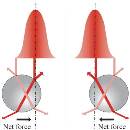
[image:18.595.199.419.317.536.2]be understood using a ray optics approach, see gure 1.1.
This shows a sphere in a Gaussian beam and how it reects and refracts light. If the gradient force, due to the refracted light, is stronger than the scattering force, due to the reected light, the particle will feel a net force towards the center of the beam.
For smaller particles (Rayleigh regime r < λ) we can not use ray optics
approach. Instead we consider the particle's polarisability. When a polarisable particle is placed in an electric eld a dipole is set up within the particle. This dipole will feel a force if there is a gradient in the electric eld, towards the stronger electric eld and hence towards the higher optical intensity. Again there is a scattering force due to reections, so the particle is only trapped when the gradient force is stronger than the scattering force.
1.2.1
Particle tracking
Many of the experiments in the thesis rely on the tracking of the movement of colloidal particles under various forces. This was accomplished using a particle tracking program called StAT written in LabVIEW by Graham Milne.
Figure 1.2: This gure shows a screen shot of StAT tracking particles. 5µm
colloid can be seen marked with red boxes that show the program has recognised them.
[1] Feynman RP. There's Plenty of Room at the Bottom. Talk given at the annual meeting of the American Physical Society 1959.
[2] Krauss TF, DeLaRue RM, Brand S. Two-dimensional photonic-bandgap structures operating at near infrared wavelengths. Nature 383 (6602): 699-702 OCT 24 1996
[3] Harrison JD, Manz A, Fan Z, Ludi H, Widmer HM. Capillary Elec-trophoresisand Sample Injection Systems Integrated on a Planar Glass Chip. Anal Chem 1992 Vol 64 p1926-1932.
[4] Harrison JD, Manz A, Fan Z, Fluir K, Fan Z, Eenhauser CS. Microma-chining a miniaturized capillary electrophoresis-based chemical analysis system. Science 261 p895-897
[6] Ramsey JM. MIC, Technical University of Denmark, http://www.mic.dtu.dk/research/microtas/microtas.htm
[7] Manz A. Imperial College London,
http://www.achem.ic.ac.uk/Web2002/zentral20group%20page.htm
[8] van den Berg A. The Lab-on-a-Chip Group, University of Twente, http://www.mesaplus.utwente.nl/mutas/bios/index.php
[9] Harrison JD. Department of Chemistry, University of Alberta, http://www.chem.ualberta.ca/faculty/harrison.htm
[10] Lab on a Chip, Published by the Royal Society of Chemistry, Chairman Manz A.
[11] microTAS, a virtual journal on micro Total Analysis Systems, Edited by van den Berg A.
[12] microTAS 2003, http://ww.mictotas2003.org/
[13] Microuidics, Physics and Chemistry of,
http://.grc.org/programs/2003/microu.thm
[14] Caliper, http://www.calipertech.com/
[15] Agilent, http://www.chem.agilent.com/Scripts/PDS.asp?lPage=51
[16] Agilent Bioanalyzer 2100 applications,
http://www.chem.agilent.com/scripts/LiteratureResults.asp?iprodinfotype= 4&1115
[18] Happel and Brenner, Low reynolds number hydrodynamics, Prentice Hall (1965)
[19] Ashkin A, Dziedzic JM, Bjorkholm JE, Chu S, Optics Letters, 11, 288 (1986)
[20] Hughes M.P., Nanoelectromechanics in engineering and biology, CRC Press (2003).
Microgears
2.1
Introduction
2.1.1
Rotating microgears with optical forces, the state of the
art
Since they were rst demonstrated in 1986 [1] optical tweezers (see section 1.2) have rapidly developed into a diverse research area giving physicists and biologists control over the micro world. No longer just used to move particles around, optical tweezers have formed a comprehensive micro tool kit. One valuable tool is the ability to rotate or align micro particles to a particular direction.
and micro Total Analysis Systems (microTAS). Here it is envisioned to per-form experiments that were traditionally carried out on macroscopic samples in centralised laboratories, on tiny volumes of analyte on a microuidic chip. They could also be used to help mixing which is a problem as discussed in section 1.1.4.
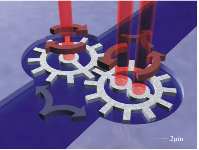
Figure 2.1: A microgear pump. Silicon microgears are optically tweezed by a rotating light pattern (red arrows) driving uid through the chan-nel (blue arrows).
2.1.2
Gradient force
An asymmetric particle can be rotated by the optical gradient force (see sec-tion 1.2) with a rotating light pattern. The principle of this idea has been demonstrated [3] but not applied to any specic applications. The motivation for this work was to create an optically powered micropump (see gure 2.1).
2.1.3
Scattered light
The second group depend on the scattering of light from an appropriately shaped object (similar to a propeller in a uid) to use radiation pressure as the driving force [4, 5, 6]. This approach has the advantage of simplicity as no complicated light pattern is required. It suers from the drawback of not being able to precisely rotate the microgear or align it but to only spin it at a speed controlled by the input power. The scattering forces also push the particle away from the focus of the laser beam reducing the quality of the optical trap.
2.1.4
Transfer of angular momentum
particle will rotate. This method has the advantage over OAM that there is no associated absorption to cause heating which is a problem when high powers are used.
Figure 2.2: A Photonic Crystal MicroGear (PCMG). The one dimensional photonic crystal in the center of the microgear refracts light ain-sotropically, along and across its slots, creating birefringence. The pitch of the photonic crystal is given by A whilst the ll factor is B/A.
quartz is not trivial. Birefringent microlenses and microprisms have been re-alised by creating in plane birefringence in a polymide. This is achieved with a curing process that aligns rod like structures within the polymide lm, how-ever the birefringence achieved is only ∆n = 0.05[7]. Another solution to the
problem is to transfer angular momentum from light to an arbitrary shaped birefringent particle which is close to the microgear. The rotating particle causes uid ow that rotates the microgear [8]. A more elegant approach how-ever, is to use form birefringence. Here we create slots in the material that are roughly the same size as the wavelength of light (a one dimensional Photonic Crystal (PC), see gure 2.2). The light propagates preferentially along the slots to across them creating an articial birefringence called form birefrin-gence. This allows the use of any material convenient for microfabrication and also can give a birefringence of up to ∆nef f = 0.5, higher than found in
natu-rally birefringent materials such as calcite ∆n= 0.16(see section 1.2). In this
2.2
Simulation
2.2.1
FIMMwave simulations
The magnitude of the birefringence was modeled using a vector mode solver (FIMMWAVE, Photon Design). This located the Fundamental Transverse Electric (FTE) and Fundamental Transverse Magnetic (FTM) modes of the 1D photonic Crystal lattice. FTE was dened as having the polarisation aligned with the slots and FTM as having polarisation across the slots. The dierence between the eective refractive indices of the two modes is taken to be the birefringence ∆nef f. Figure 2.3 shows simulated FTE and FTM modes. Here
the slots run horizontally and it is clear that the FTM mode (a) is more evenly spread across the slots, whereas, the FTE mode (b) is better conned. The connement is in the higher refractive index parts of the slots, the microgear material rather than the medium they are suspended in, making the FTE mode see a higher nef f.
Figure 2.3: Simulated form birefringence of a microgear. The slots in the cen-ter of the microgears are simulated as a one dimensional photonic crystal lattice. The Fundamental Transverse Magnetic (FTM, a) and Fundamental Transverse Electric (FTE, b) modes are located. This plot shows the magnitude of the electrical eld with yellow showing areas of high eld.
The exchange of momentum between the light and the microgear due to the birefringence exerts a torque, τ, on the microgear given by [10];
τ ∝Eo2[1−cos(kd∆nef f)] (2.1)
Where Eo is the electric eld, k is the wave vector, d is the microgear's
thickness and∆nef f is the birefringence. From this it can be seen the maximum
torque will be achieved atd∆nef f =λ/2, when the particle acts as a half wave
plate. Circularly polarised light has SAM of ±~per photon. If passed through
a half wave plate the light will be changed into circularly polarised light of the
other handedness giving 2~ angular momentum to the microgear per photon.
As our value for d∆nef f is less than a tenth of the value for a half wave plate
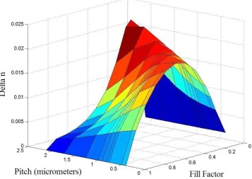
Figure 2.4: Form birefringence as a function of pitch and ll factor, simulated for Su-8 in water. As the pitch increases so does the maximum form birefringence. The optimum ll factor changes with pitch.
2.3
Optical Setup
The sample cell containing the microgears was placed into a simple optical tweezing setup shown in gure 2.5. The sample cell consisted of a microscope slide and a cover slip separated by a vinyl spacer. The laser used was an IPG Photonics bre laser operating at 1070nm with a max power of 10W. This was focused down to a spot 5µm in diameter. Laser powers up to one Watt were
used as it was found that at higher powers the radiation pressure (see section 1.2) pushed the microgears against the microscope slide causing friction that hindered the microgears rotation.
The microgears are optically trapped in two dimensions allowing them to be moved around horizontally in the sample cell and then rotated in one of two ways. Either using circularly polarised light (use the Quarter Wave Plate (QWP)), or with linearly polarised light that has had its direction of polari-sation rotated (by rotating the Half Wave Plate (HWP) in a rotating mount). The rotation of the microgears was observed on a CCD camera and videos were recorded for analysis.
2.4
Fabrication
2.4.1
Microfabrication techniques
Microgears have been created for optical manipulation in a number of dierent ways. The most popular fabrication method is two photon polymerization [3][4]. Here light is focused tightly into a photocurable resin which absorbs two photons in a single quantum event polymerizing the resin into a hard shape which is dened by moving the focus of the beam within the resin. As the two-photon absorption is proportional to the square of the light intensity the area of polymerization is small compared to the optical spot size allowing the fabrication of features down to 100s of nm.
Other methods include photolithographic lifto [8], conventional MEMS fabrication techniques [5] and commercial MEMS fabrication [6]. Microcom-ponents have been made from a birefringent polyimide lm by electron beam lithography and reactive ion etching [7]. Soft lithography has also been used to create PDMS microgears [11] which could have been optically driven but were magnetically driven. Which fabrication method is most suitable depends primarily on the material that the microgears are to be made from and the minimum feature size of the microgears.
Silicon was chosen as the microgear material as it has a high refractive index which gives a high refractive index dierence between the microgear and the medium it is put into. This gives a high optical gradient force (see section 1.7) and hence a strong interaction with an optical pattern. The rst microgears were designed to have circles of material in their centers that could be grabbed by this force and rotated by rotation of the optical pattern (see gure 2.1).
mi-crometer size range. We chose to use two methods to pattern material on these length scales, photolithography and electron beam lithography. These techniques have the advantage of being widely available and well understood due to their use in the construction of microprocessors. Two photon polymer-ization has the advantage of being able to easily construct 3D features but is not compatible with mass fabrication so is unlikely to become as popular. Features down to two micrometers can be made using photolithography whilst the e-beam lithography system at St Andrews can go down to 16nm but has the drawback of being more technologically demanding. To construct a gear that could be moved using optical tweezers it is desirable to make features that are smaller than two micrometers hence it is necessary to use electron beam lithography whilst photolithography could be used to construct channels for the microgears to spin in. For an explanation of photolithography see section 3.2.1.
2.4.1.1 Electron Beam Lithography (EBL)
Electron beam lithography (EBL) involves the exposure of a thin layer of polymer, the resist, to a focused beam of electrons. The resist is chosen and prepared so that the electron beam eects its solubility. In a positive resist the polymer chains in the exposed areas are cut by the beam making it more soluble When the sample is placed in a developer these areas are washed away. In a negative resist the exposure cross-links polymer chains so that they are less soluble and when it is placed in developer the unexposed areas are washed away (see gure 2.6).
Figure 2.6: A pattern of microgears that has been written using Electron Beam Lithography (EBL). Here PMMA, a positive resit, has been used so the areas around the microgears have been exposed and hence removed when the sample was developed.
being written in series, but this also gives it exibility allowing the design to be changed easily giving fast prototyping. The high resolution also comes at a high nancial price with the high precision system being expensive to purchase and to maintain due to its complexity.
see section 2.4.3.2, for electrons scattering and the proximity eect see section 2.4.4).
2.4.1.2 Reactive Ion Etching
Transfer of the pattern from the resist into the microgear material was per-formed by Reactive Ion Etching (RIE) in a home built RIE setup. The process of RIE involves exposing areas of material that are to be removed to a plasma of a gas that will chemically react with this material forming a volatile gas. Ions are accelerated towards the sample to make the etching anisotropic, giv-ing vertical side walls. Areas covered by the resist are not aected by the plasma so remain. The resist will be eroded by the plasma but by choosing the chemistry wisely a combination of gas, material and resist can be found to give good selectivity (the selectivity is dened as the thickness of material removed divided by the thickness of resist removed). The key parameters in RIE are the power used and the pressure the etching is carried out at. How these parameters aect the dierent etching and the dierent recipes used will be discussed in the relevant chapters.
2.4.2
Silicon microgears
2.4.2.1 Using PMMA as an etch mask
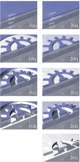
and lifting o technique is similar to a previously used microgear fabrication technique [6]. For this process to work a thick enough layer of resist is needed so that the silicon can be etched away before the resist. If this is not possible then a two mask process is required where the pattern is transferred from the resist into a hard mask that is then used as a mask to etch the microgear material.
The two processes are shown in gure 2.7. First PMMA is spun on (1(a), 2(a)) and patterned by EBL (1(b), 2(b)). The pattern is then transferred into the silicon in a one step process 1(c) or into a hard mask for a two step process 2(c). This hard mask is then used to pattern the silicon 2(d) before the microgear is released (1(d), 2(e)).
A sample of microgears patterned into 130nm thick PMMA on SOI was obtained from the University of Glasgow. The silicon on top of the SOI was 330nm thick so a selectivity of three was required to be able to use the PMMA as an etch mask. A series of experiments were conducted to nd the optimum conditions for high selectivity (see appendix 2.7.1). It was found that the maximum selectivity achievable was 1.2 so it was necessary to go to a two step mask method using PMMA and silica as masks.
2.4.2.2 Using silica as an etch mask
The etching of the resist is due more to physical bombardment of ions from the plasma than it is due to actual chemical etching. Thus to etch deeper into the silicon a harder mask that will not be eected by either the physical or chemical etching is needed. Using silica as an etch mask, a much higher selectivity can be achieved. Although silica can be etched using uorine chemistry (the uorine in CHF3 reacts with the Si in SiO2 to form the volatile gas SiF4) it etches
transferred from PMMA into silica it can then be transferred from the silica into the silicon (see gure 2.7). SOI coated with 100nm of silica was obtained and 130nm of PMMA was spun on and patterned by EBL. The pattern was transferred into the silica using CHF3 at 0.03 mbarr, 33W with the gas ring
at position 30mm for 15 minutes. This removed almost all of the resist giving a selectivity of 1 but as the layer of silica is thinner than the resist, this is all that is needed. The pattern was then transferred into the silicon with SF6 at
When the microgears were put into an optical trapping setup they were not attracted to the light as they had been designed to, but were repelled by the areas of high intensity. This can be seen in gure 2.10 which is a series of images taken from a video of a silicon microgear.
2.4.3
Polymer microgears
SU8 photoresist (2000.5 and 2050, MicroChem) was chosen to be used as a microgear material due to its refractive index of 1.56. This index reduces the scattering forces making it more likely for the microgear to be attracted to an optical trap. SU8 is easily processed, it can be spun onto a substrate into nearly any thickness desirable and patterned by either photolithography or EBL.
2.4.3.1 Direct Writing
The simplest way to create microgears in SU-8 is to directly write into the SU-8 layer with EBL. The process is shown in gure 2.11 with the substrate being spin coated in release layer then SU-8 (gure 2.11,1(a)), the SU-8 being patterned by EBL (gure 2.11, 1(b)) and then the release layer being removed (gure 2.11, 1(c)). SU-8 acts as a negative resist for EBL so that the areas of the microgear that we want to remain are exposed to the electron beam. A silicon substrate was coated in a release layer (SU-8 release layer, MicroChem, spun at 3000rpm for 60s then baked on a hot plate at 200oC for 60s) then in a
350nm layer of SU8 (SU-8 2000.5 spun at 5000rpm for 60s, hot plate at 100oC
for 60s) and patterned by EBL. After the exposure the resist needs a further bake, 30s at 100oC, to ensure full polymerization. The resist was developed in
2.4.3.2 EBL exposure parameters
Figure 2.12: EBL exposure. This gure shows how the beam in the EBL system moves. It follows the red line in a vector scan stopping at points separated by the area step size, s.
The dose is how many electrons hit the resist per unit area measured in
µAs/cm2. Usually a negative resist is used and the dose required to break
enough of the polymer chains making the resist soluble is called the clearing dose. Writing in SU-8 we expose the areas we wish to keep by cross linking the polymer chains. The beam moves along the desired pattern as shown in gure 2.12 in what is called a vector scan. It moves a distance dened by the area step size and waits for a time called the dwell time. The dose is then given by;
Dose= IbeamTdwell
s2 (2.2)
Where Ibeam is the current of the electron beam, Tdwell is the dwell time
ands is the area step size. The electron gun gives a constant beam current for
2.4.3.3 Using FOx-12 as a hard etch mask
Figure 2.14: An SU8 microgear. Microgears were created that closely resemble the desired design by patterning FOX12 then using this as an etch mask to pattern the SU-8.
make the microgear thicker than can be achieved just with SU-8 type 2000.5 a mixture of type 2000.5 and type 2050, that can be spun on between 15 and 100
µmthick, was used. The mixture used was 10:1 2000.5:2050 and it was spun at
1000rpm for 60s to give a1µmthick layer. It was the exposed to UV radiation
to cure it and baked at 100oC 60s then 240oC 60s (SU-8 does not need to be
baked at this high a temperature to cure it but FOx-12 does and it is good practice to bake lower layers at the same temperature as higher layers so that no solvent is released in subsequent hotter bakes). However the FOx-12 did not spin on into a uniform layer on top of the SU-8, instead it formed droplets as water does on a hydrophobic surface. Various parameters in the treatment of the SU-8 layer were tried such as baking it for longer and exposing it for longer to see if its surface could be changed enough to allow the adhesion of the FOx-12. It was found to be necessary to expose the SU-8 to a oxygen plasma for 30s to roughen the surface before a good lm of FOx-12 could be spun on. The spinning parameters used were 5000 rpm for 60s then baked for 2 min at
100oC then 2 min at 240oC. The FOx-12 was then patterned by EBL using
the an acceleration voltage of 20kV, 30 micrometer diameter aperture, area step size 20nm, area settling time 0.05. It was developed in MF319 (Shipley) for 60s, washed in 10:1 water:MF319 for 15s followed by water for 15s. This creates a hard mask of 60 to 70nm thick that can subsequently be used as an etch mask for the SU-8 underneath using RIE with an oxygen plasma. The etching parameters were oxygen at 0.027 mbarr, power 30W, ring at position 30mm for 3 minutes (for a discussion of how these parameters eect RIE see section 2.7.1). The FOx-12 is very tough against this attack giving a very high selectivity so that SU-8 layers as thick as 2 µm could be processed with 60-70
2.4.4
Photonic Crystal MicroGears (PCMG)
A more elegant rotation method would be to use birefringence. As naturally birefringent materials are dicult to pattern we thought of the possibility of creating the birefringence articially using form birefringence. Here birefrin-gence is created by shaping the centers of the microgears into a series of slots with a period similar to the wavelength of light (a 1D photonic crystal). As the light passes through the slots it sees dierent refractive indices depending on whether it is polarised along or across the slots (see section 2.2).
Photonic crystals are usually created by etching a lattice of holes into a semiconductor and used amongst other things to guide light via a photonic band gap [14]. For form birefringence we do not use the photonic band gap which is only evident in the horizontal plane of the crystal but instead illumi-nate the crystal from above akin to a Photonic Crystal Fibre (PCF). When constructing the photonic crystal the ll factor and pitch are critical for this application. The pitch can be chosen and accurately written by EBL but the ll factor can vary with the dose. As writing in FOx-12 was more tolerant to changes in the dose this method was used to create Photonic Crystal Micro-Gears (PCMG).
Process 2 in gure 2.11 was used but even with this more dose tolerant approach the optimal dose for the same pattern changed from run to run (see gure 2.17).
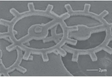
Figure 2.15: This coloured electron micrograph shows a microgear that has been created by patterning FOX12 by EBL then transferring the pattern into the SU-8 by RIE with oxygen.
Figure 2.16: This diagram shows a layer of resist being exposed to an electron beam of 20 or 30kV. The electrons represented by arrows are both forward scattered by a small angle (a) and back scattered by a large angle (b).
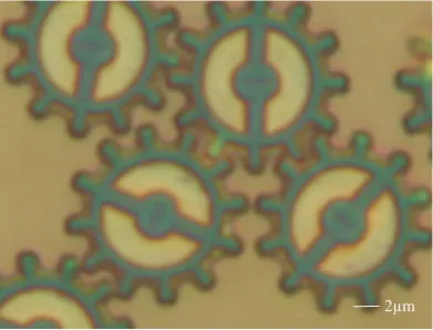
This improvement in consistency was necessary as many microgears were required to account for the wastage resulting from the process of releasing the microgears and transferring them into the optical set up. After the microgears were released in NMP the sample was washed in water and then repeatedly dipped into a drop of water placed onto a microscope slide causing a few of the microgears to go with the water onto the slide. Since most of the microgears stay near to the substrate after release, only about one percent of the microgears made can be tested. If this process could be made more ecient then a varying dose would not be a problem as enough microgears of dierent doses could be written in a short enough time. The small variation in dose allowed the creation of microgears good enough to test (see gure 2.15) so these microgears were released from the substrate and tested (see section 2.5).
Figure 2.18: Each picture is the optimal dose from a dose test using the same pattern with the aperture changed to 30 micrometers diameter. The dose is now more consistent.
need to be transported onto a microscope slide before testing. Another way to improve the writing may be to fully cure the FOx-12 layer and instead pattern a PMMA layer on top of it and use this as an etch mask to etch through the PMMA layer. This would help if the writing is more consistent in PMMA than FOx-12 but it does have the drawback of adding another step to the fabrication process. Another disadvantage is that PMMA is a positive resist so the area around the microgear would have to be written instead of the microgear increasing write times.
2.5
Results
[image:59.595.107.507.207.488.2]2.5.1
Circularly polarised light
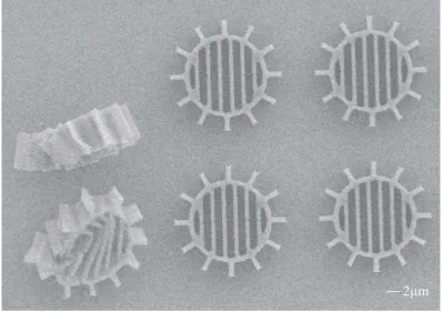
Figure 2.20: These microgears have been damaged by the stylus proler show-ing that they hold together well when a force is applied and also shows their depth.
laser power (gure 2.21,a). When illuminated with a linearly polarised laser beam the microgears aligned themselves with the direction of polarisation and followed the polarisation direction upon rotation. As the half wave plate is rotated in the beam path the polarisation is rotated through twice the angle which means the microgears rotate at twice the frequency of the half wave plate. The maximum rotation rate achievable before the microgears could not follow the direction of polarisation due to frictional forces was proportional to the laser power. At powers of higher than one Watt, the microgears were pressed down onto the surface of the sample cell. This introduces another source of friction and prevents the free rotation of the microgears.
The magnitude of the variation of the transmitted light was compared to the absolute magnitude of the light giving the birefringence (see gure 2.21,b). This was measured as ∆nef f = 0.015±0.001 for a microgear with a lattice of
pitch 0.8µm and ll factor 0.3. For the same lattice the simulated birefringence
is ∆nef f = 0.018±0.001, which agrees well with the measured result.
2.6
Summary and Outlook
We have shown that Spin Angular Momentum (SAM) can be transferred from circularly polarised light to a form birefringent microgear causing the micro-gear to rotate. The micromicro-gears readily align themselves with the direction of polarisation of linearly polarised light allowing them to be precisely orientated or rotated by rotating the direction of polarisation of the light. As the shape and birefringence of the microgear can be controlled, they may nd applica-tions in microrheology experiments. For applicaapplica-tions in the Lab-on-a-Chip area the angular momentum transferred from the photon to the microgear will have to be increased. This could be done by increasing the birefringence (see section 2.6.1) or by making each photon pass through the microgear many times (see section 2.6.2).
2.6.1
Increasing the birefringence
From equation 2.1 we can see the optimal condition for getting torque form the light is for the microgears to have ∆nef fd= λ2. The fabricated microgears have
a∆nef fdof less than one tenth of this value. Figure 2.23 shows how the torque
varies with ∆nef fd taken from equation 2.1. This shows that although the
present∆nef fdis one tenth of the optimal value the torque could be increased
by 100 times. ∆nef fd can be increased by either increasing the thickness of
Figure 2.23: The torque on a microgear of dierent ∆nef fd.
be achieved by increasing the refractive index of the microgear material to that of silicon, 3.5. However there is a problem, as increasing the refractive index increases the scattering forces due to reections so that the particle is no longer held in the 2D optical trap (see section 2.4.2). One possible solution to this problem is using an antireection layer to reduce the reections from the silicon.
Figure 2.24: A The dotted line represents the reection from a water/ n2
in-terface. The solid lines show the amount of reection that will cause attraction or repulsion. B shows a close up of the refractive indices that will cause attraction. C shows the reection from a water silicon interface if an AR coating of λ
4 thickness and
refrac-tive index n1 is used. D shows the reection from a OptiNDEX A14 coating of dierent thicknesses.
this point and anything above this line will be repelled by the light. More experiments would be needed to nd if a refractive index between these lines causes attraction or repulsion. The dotted line shows the fresnel reections from a water n2 interface. This tells us that unless we reduce the reections
from the silicon microgears from their 20 percent value given by Fresnel's law to below 7.5 percent, they will not be attracted and if we reduce them to less than 6 percent they will be. Figure 2.24B shows a close up section gure 2.24A so that the small ranges of refractive indices that cause attraction above the reection line can be seen.
Figure 2.24C shows the amount of light that would be reected from a water silicon interface if an antireection (AR) coating λ
4 thick of refractive
index n1 was used. This was calculated using the fresnel reection formula and shows that to get zero reection an AR coating of refractive index 2.2 should be used. It also shows that if OptiNDEX A14 was used (refractive index 1.95) a reection of just 1.4 percent could be achieved.
Figure 2.24D shows how much reection would be given from an OptiNDEX A14 AR coating of various thickness. Again it is calculated using the Fresnel reection formula and tells us how tolerant the AR coating is to thickness variation. It shows us that if the coating is between 100 and 175 nm the reections will be less than 6 percent. This should be achievable by a spin coating process.
2.6.2
Multiple pass systems
Figure 2.25: A microgear in a cavity. This diagram shows a microgear in a cavity formed by two mirrors that give π phase change on
reec-tion and includes two phase plates that give 3π/4 phase change
to correct the polarisation state of the light.
the lower phase plate it is converted back to circularly polarised light but with the handedness changed so that it pushes in the same direction as the light going down. The cycle then continues for as long as the light stays in the cavity. As it is possible to create cavities with large Q values it could be possible to increase the momentum transferred from the light by several orders of magnitude.
2.6.3
A new way to make the world go ’round?
Sections 2.6.1 and 2.6.2 show ways to increase the amount of power that is transferred from the light beam to the microgear. This section will look at how much these techniques can increase the power given to the microgear, could this be a new way to harvest power from light?
At rst appearance this technique seems very poorly suited to the genera-tion of power as we have only demonstrated the rotagenera-tion of a microscopic gear and it requires 1W (a lot of power) to induce a fairly pedestrian rotation rate of 60rpm. However as we have seen, there are several things we could do to improve this and as power harvesting is such an important area of research, it is interesting to consider angular momentum transfer as a source of power. The momentum transferred from the light to the microgear depends on the microgear's birefringence (see equation 2.1) and is a maximum of 2~per
pho-ton when ∆nef fd = λ2. This represents the maximum amount of energy that
can be passed from the light to the microgear as the light passes through it. However it is possible to send the light through the microgear more than once by putting it in a optical cavity. Here the light would pass through the
micro-gear many times giving up to 2~per photon momentum each time. Comparing
a cavity with a Q of around1014would be needed to match solar cells and then
the power would still need to be converted into electrical energy. Although no light is absorbed as it passes through the microgear, there will be a practical limit to the Q value due to the scattering form the microgear and this is sure to be below 1014. This shows that power harvesting is not a good application
[image:69.595.110.504.264.547.2]for this technology.
2.6.4
Conclusion
This work clearly shows that form birefringence has potential applications for actuating micromachines such as a micropump (see gure 2.26) or to create tools to use in biological experiments even though very little power is trans-ferred from the beam to the microgear. Future work should focus on;
Varying the pitch and ll factor of the photonic crystal to check the birefringence changes as the simulations suggest.
Increasing the birefringence of the microgears by using higher refractive index material.
Increasing the torque per incident photon by creating a cavity.
2.7
Appendix
2.7.1
Reactive Ion Etching
To fabricate microgears from silicon on insulator (SOI) it is necessary to etch through 330 nm of silicon. First we tried a 130 nm layer of PMMA as the etch mask, so a selectivity of roughly 3 was required. To nd how the dierent etching parameters aected this selectivity, a series of experiments was carried out with photoresist S1818 as an initial mask. In each case the photoresist was prepared to the same recipe, spun at 5000rpm for one minute, baked at
100oC for 1 min, exposed for 3 minutes and developed for 3-5 minutes. The
rst parameters tried were SF6 at 3 Pa (0.03 mbar), gas ring at position 0 (the position where the gas ring is furthest from the sample) and powers from 7 to 50W for one minute (see gure 2.27).
Figure 2.27: This graph shows how the etching rate and selectivity vary with etching power for SF6 and silicon.
Using this information, a sample of PMMA on SOI was etched at the same conditions as above but low power (10W). The selectivity was found to be 1.2, not enough for our etching. The next parameter to be investigated was pressure. SF6 was used with 20 W power, ring at position 0, pressures from 3 to 1.6 Pa (0.03 to 0.016 mbar) for 2 minutes (see gure 2.28).
Figure 2.28: This graph shows how the etching rate and selectivity vary with etch pressure for SF6 and silicon.
From this it can be seen that decreasing pressure increases selectivity but only by about one third. For pressures below 1.6 Pa (0.016 mbar), a stable plasma could not be achieved. Silicon is often etched with a mixture of SF6 and CHF3 as the CHF3 pacies the side walls of the etch, improving directionality. To see if this increased the selectivity at all, samples were prepared as before and etched with dierent mixtures of SF6 and CHF3. The etch parameters used were 20 W of power, etch pressure 3 Pa (0.03 mbar), ring height 0, a mixture of SF6 and CHF so that the SF6 varied from 10 to 100 percent and a time of 2 minutes (see gure 2.29).
Figure 2.29: This graph shows how the etching rate and selectivity vary with the amount of SF6 in the SF6/CHF3 mix.
would reduced the photoresist etch rate. However as Argon was not available Nitrogen was used instead. Etching was performed with 10W power, at 3 Pa (0.03 mbar), ring at position 0 for 2 minutes with gas composition from 10 to 90 percent SF6 (see gure 2.30).
Figure 2.31: This graph shows how the etching rate and selectivity vary with concentration of SF6/CHF3 and N2.
This shows that although adding nitrogen did decrease the photoresist etch rate the end result was a decrease in selectivity. To check that the same trend would be evident for a mixture of SF6/CHF3 and nitrogen, a set of samples were etched with the same amount of CHF3 to SF6 but dierent amounts of nitrogen. The conditions used were 10 W power, 3 Pa (0.03 mbar), ring at position 0, and gas compositions of 10 to 90 percent SF6/CHF3 (see gure 2.31). The samples were etched for 6 minutes to increase the amount etched and increase the accuracy of the measurements.
From this it can be seen that again the addition of nitrogen only decreases the selectivity. As the addition of nitrogen had disappointing results the ability to use argon was added to the etching setup to see if it would have a more benecial eect. A set of samples were etched at 10 W, 3 Pa (0.03 mbar), ring at position 0, with from 10 to 90 percent SF6/CHF3 in the SF6/CHF3/Ar mix (see gure 2.32).
Figure 2.32: This graph shows how the etching rate and selectivity vary with concentration of SF6/CHF3 and Ar.
of 120nm with a 120nm layer of PMMA giving a selectivity of 1 which is not as good as before just using SF6. One more parameter was available to vary, the height of the gas ring. A set of samples were etched with SF6 and CHF3 at 10 W, 3 Pa (0.03 mbar), with ring ring lowered from 0 to 40 mm towards the sample for 6 minutes (see gure 2.33).
This shows that the height of the ring does not signicantly eect the selectivity of the etching. Hard baking the PMMA before etching was also
tried. A sample was baked at 90oC for 30 minutes before etching but no
[1] Ashkin A, Optics Letters 11 288 (1986).
[2] Bishop AI, Nieminen TA, Heckenberg NR, Rubinsztein-Dunlop H, Phys-ical Review Letters, Vol. 92, No. 19 198104-1 (2004).
[3] Maruo S, Ikuta K, Korogi H. Journal of Microelectromechanical Systems, Vol. 12, No. 5, 533 (2003).
[4] Galajda P, Ormos P. Applied Physics Letters Vol. 78 No. 2 249 (2001).
[5] Higurashi E, Ohguchi O, Tamamura T, Ukita H, Sawada R. Journal of Applied Physics, Vol. 82, No. 6, 2773 (1997).
[6] Gauthier RC, Tait RN, Ubriaco M. Applied Optics Vol. 41 No. 12 2361 (2002).
[7] Higurashi E, Sawada R, Ito T. Journal of Micromechanics and Microengi-neering, Vol. 11, 140 (2001).
Ap-[9] Nieminen TA, Heckenberg NR, Rubinsztein-Dunlop H. Journal of Modern Optics, Vol. 48, No. 3, 405-413 (2001).
[10] Friese MEJ, Nieminen TA, Heckenberg NR, Rubinsztein-Dunlop H, Na-ture 394, 348-350 (1998).
[11] Ng JMK, Fuerstman MJ, Grzybowski BA, Stone HA, Whitesides GM. J. AM. CHEM. SOC. Vol. 125, No. 26, 7948 (2003).
[12] McCord MA, Introduction to Electron-Beam Lithography, Short Course Notes Microlithography, SPIE's International Symposium on Microlithog-raphy, p63, 14-19 March, (1999)
[13] Rai-Choudhury P. Handbook of Microlithography, Micromachining, and Microfabrication: Volume 1. SPIE.
[14] Krauss TF, Physics World, 19 (2), 32-36, (2006).
Optical Sorting
3.1
Introduction
The controlled manipulation of colloid is critically important not just for the study of the physics of colloidal suspensions, but also for medical science, where we can replicate a biological suspension with a colloidal one. One important device in the control of colloidal suspensions is a sorter. A sorter allows the purication of a sample and could be used, for example, to separate a pure population of stem cells from all the other species of cell found in a blood sample. A sorter could also be used to sort one cell type from another so that they may be counted. This may help with tests such as a Complete Blood Count (CBC), which is a count of the dierent types of cells in a blood sample, and is a vital piece of information in monitoring a patients health.
Sorting (MACS), or active sorting methods such as Fluorescence Activated Cell Sorting (FACS). Of these, the state of the art technique is FACS, so we will look into the mechanism of this technique in more detail.
[image:80.595.157.460.250.567.2]3.1.1
State of the art, Fluorescence-Activated Cell Sorting FACS
Figure 3.1: Diagram of a FACS machine. This shows a population of uores-cence labeled cells (green circles) and non labeled cells (red circles) being hydrodynamically focused, interrogated, charged then elec-trostatically deected.
only one cell wide. The cells then pass through a laser beam that excites u-orescence if the cell is tagged, which is then picked up by the detector. The stream is then split into droplets, with just one cell in each droplet. A PC con-nected to the detector charges each droplet depending on whether the detector has detected a uorescent cell, a non uorescent cell or no cell. The droplets are then electrostatically deected by charged plates into one of three tubes depending on their charge. Although this is a serial process with only one cell at once being sorted, the state of the art machines can process up to 50,000 cells per second. However the instruments are complicated, expensive and re-quire trained dedicated sta and as such can only be found in hospitals and research institutes [1]. There is an increasing interest in miniaturizing these technologies onto an 'Lab-on-A-Chip' (LOC) platform [1][2][3][4]. This would allow the creation of a point of care device that could be used in a doctors surgery or even at home.
In this chapter I will present an optical sorting approach that uses the dierent optical properties of particles to sort them with an optically induced force. This has advantages of being able to sort particles over the area of a channel instead of one at a time and is elegant, using the optical properties of the particles to dierentiate them and move them. An example is separating red and white blood cells that due to their dierent shape and size exhibit dierent optical responses. Sorting techniques such as these will be essential in ensuring LOC products such as Agilent's Bioanalyzer reach their full potential [5].
Figure 3.2: Optical Sorting. The blue arrows show the direction of uid ow and the red arrow indicates optical forces. The mixed colloid enters by channel A and water by channel B. The smaller colloid experi-ences forces from the optical pattern E moving it into channel D whilst the larger colloid goes straight through the optical pattern and out channel C.
3.2
Fabrication of a microfluidic flow chamber
To help demonstrate the fractionation of colloid using an optical lattice I de-veloped a fabrication process for creating microuidic ow chambers. I tested two methods of fabrication. The rst method involved constructing channels in SU-8 on a substrate by photolithography. These were then sealed by gluing them to a cover slip (see section 3.2.2). The second method involved casting channels of Poly(dimethylsiloxane) (PDMS, Dow Corning) using a soft lithog-raphy method and then bonding the PDMS to a glass cover slip (see section 3.2.3. Both methods rely on photolithography so it is necessary to discuss this technique.
3.2.1
Photolithography
out on a Karl Suss MJB-3 mask aligner that operates at 405 nm (Hg H-line) and 365 nm (I-line). This machine is used to align the pattern on the mask to any feature that may already be on the sample and to ensure the correct pressure is applied between the mask and the sample. This is called contact lithography as the mask comes into contact with the photoresist. The correct pressure ensures that there is no gap between the mask and the resist, that could cause a broadening of the features, without causing damage to either the sample or the mask. This is an important parameter for good reproducible photolithography. Another possible cause for a gap between the mask and the resist comes from a non-uniform resist layer. The resist is typically spun onto the material which can cause a build up of resist at the edges of the sample called an edge bead. This is a particular problem for high viscosity photoresists that give thick lms and the edge bead must be removed for a good result. I have found that the easiest way to remove edge beads from a positive resist is to expose the edges and develop the resist around the edges away. I have found no similarly neat technique for dealing with a negative resist (SU-8) but this is rarely a problem as it is typically used for microuidic channels where the critical dimensions are large. The exposure times and doses used are discussed later in the dierent fabrication recipes.
3.2.2
SU-8 microfluidic channels
SU-8 2050 (MicroChem) was spun onto a cover slip at 1250 rpm for 60 s to give the desired thickness of100µm. This was then patterned by photolithography
Figure 3.4: Channels fabricated using the gluing method. A) A good contin-uous channel. B) A channel blocked with glue.
it will ll the channels. The adhesive was then exposed to UV radiation to cure it. The resulting channels can be seen in gure 3.4. This method proved to be unreliable with no spin speed found to produce an amount of glue that would work every time.
3.2.3
PDMS microfluidic channels
3.2.3.1 Lift-off
To create a negative of the mask, a lift-o technique was used. The simplest form of lift-o involves creating a pattern in photoresist onto which a metal is evaporated. When the resist is then dissolved, the gold is left in the areas where there was no resist so that the pattern is a negative of the original mask (see gure 3.5). However, as the edge of the resist tends to form a slight curve instead of a vertical wall, there can often be a continuous layer of gold from the substrate onto the top of the resist. If this occurs, the gold will tear when the resist is removed, thus leaving a jagged edge to the pattern. To prevent this, a Lift-O Resist (LOR, Shipley) is used.
This is spun on before the photoresist and is baked so that it is slightly more soluble than the photoresist. The photoresist is then patterned as usual and when it is developed, some of the LOR is removed from under the photoresist leaving an overhang. This ensures that there can be no continuous layer of gold giving a crisp edge to the pattern. The critical dimension when using LOR is the size of the overhang. If there is no overhang in the resist it will give a rough edge to the gold, if however there is too much overhang, the resist will collapse onto the substrate and allow the gold to form a continuous layer, resulting again in a rough edge. It was found that an overhang of 0.5 to 1 µm
was optimal. To achieve this reliably, bake temperatures and times as well as development times were varied. It was found that the critical parameter was bake temperature with 190oC rather than the manufacturers guideline 180oC
giving the best results.
3.2.3.2 Soft Lithography
Figure 3.6: The inverted mask. LOR has been used leaving a crisp edge to the pattern. Features A and B will form inlet channels and feature C an outlet.
The mould was created in SU-8 on a glass substrate using the following recipe; SU-8 was spin coated onto a large cover slide at 1250 rpm giving a 100µm thick layer. The sample was then heated in a two stage pre exposure
bake on a hotplate at 65 oC for 5 mins then 95 oC for 5 mins. The sample
was exposed on the above mentioned mask aligner through a mask such as the one in gure 3.6 for 60s. It was then heated in a two stage post exposure bake with the same conditions as the pre exposure bake. The sample was developed in EC solvent for 9 mins and then developed again in a fresh beaker of EC solvent for 30s to nish the development. This produces a mould with the desired shape of the channels being mesas in the SU-8.
Liquid PDMS mixed in a ratio of 10:1 was then poured onto the mould
Figure 3.7: Soft lithography. A) A mould is made from SU-8 on a glass substrate. B) Liquid PDMS is poured onto the mold and cured. C) The hard PDMS is then peeled from the mould and inverted. This and a drilled coverslip are then exposed to an oxygen plasma. D) The exposed sides of the PDMS and cover slip are pressed together forming an irreversible bond.
points where the SU-8 had cracked the mould could break leaving some SU-8 in the channel thus destroying the mould (see gure 3.8).
Using a silicon substrate for the mould reduced the amount of cracking of the SU-8 and hence the mould lasted longer. The mould often looked better after rst being used as any small cracks would ll with PDMS and not be removed from the mould when the rest of the PDMS was removed. Using this mould it was possible to create channels that were an exact replica of the mask (see gure 3.8(E)). To connect the channels to a pump, glass inlets were then glued to the drilled coverslip. Norland Optical Adhesive (NOA 71) was used as it is desirable to allow the glue to enfold the whole of the inlet but then be able to x the glue before it enters the microchannels. This is possible with NOA as it is possible to x it by exposing it to UV radiation. Figure 3.9 shows a completed ow chamber.
One inlet has been lled with rhodamine and the other with blue food colouring so that the liquid in each channel can be distinguished. The insert shows a close up of the ow through the channels when pressure is applied to the two inlets, the ow direction being from left to right. It can be seen that ow through the channels is laminar with no turbulent mixing and that a small amount of diusion has occurred from one channel to the other as the boundary between the two liquids is sharper towards the left of the channel than the right. Flow cells made in this way were used in optical sorting experiments (see section 3.4). However there remains a few problems with the fabrication process. The rst is the formation of bubbles in the PDMS (see gure 3.10).
Figure 3.9: A completed ow chamber. One inlet has been lled with rho-damine and the other with blue food colouring. The inset shows a photograph taken through a microscope when there is ow through both inlets.
dose was found to be around 100s and this only caused typically one or two bubbles. The bubbles cause a problem if they are directly above the channel as they hinder imaging the channel so that some of the PDMS components made can not be used. This is not a big problem as it only takes 15 mins to make another one and PDMS is not expensive. Another limitation is the ease in which the channels become blocked (see gure 3.11).
Figure 3.10: Bubbles in PDMS. The number of bubbles depends on the ex-posure time. A) Exposed 100s, B) 150s, C) 200s, D) 250s.