Review on Low Voltage Current Conveyor
Kaushani H.Shah
1, Bhoomi P.Patel
2,Mohammed G. Vayada
3PG Student [VLSI], Dept. of ECE, Silver Oak Engineering College, Ahmedabad, Gujarat, India1 PG Student [VLSI], Dept. of ECE, Silver Oak Engineering College, Ahmedabad, Gujarat, India2 Assistant Professor, Dept. of ECE, Silver Oak Engineering College, Ahmedabad, Gujarat, India3
ABSTRACT:Now a day current mode circuits have been receiving significant attention in analog signal processing. For high frequency current mode applications is a current conveyor. In many cases the conveyor-based implementation offers improved performance to the voltage op-amp-based implementation in terms of accuracy, bandwidth and convenience.Current mode circuits do not have the limitation of dynamic range. Various topologies are used to implement current conveyor circuit. In this paper two topologies are used which are current mirror based topology and differential pair based topology. Major applications are available based on current conveyor which are capacitance multiplier, negative impedance conveyor and V to I converters. This paper gives the comparison of both topologies in terms of gain, bandwidth, linearity, power consumption. In the end results of different simulations are compared to conclude that differential pair based topology gives better results.
KEYWORDS: Bandwidth, CCII, CMOS, Current Conveyor, Gain, Linearity, VLSI.
I. INTRODUCTION
The current conveyor is a three terminal device performing many useful analog signal processing functions when the device is connected with other electronic elements in specific circuit configurations. The current conveyor has evolved from first generation to third generation. the first generation current conveyor (CCI) was proposed by Smith and Sedra in 1968 [1] and the more versatile second generation current conveyor (CCII) was introduced by the same authors in 1970 [2] as an extension of their first generation conveyor.
There has been substantial emphasis on the development of current mode signal processing circuits such as filters and oscillators. This is due to increased bandwidth, simple circuitry, better linearity, dynamic range performances and lower power consumption as compared to their voltage mode circuitry. A variety of current mode building blocks are developed with current mode circuits. The current conveyor (CCII) is one among such blocks which has received significant attention. It is hybrid block and has basic construction containing a voltage follower (VF) interconnected with either current mirror or current follower. Two topologies of the current conveyor are used. The first is based on current mirror and the second is based on differential pair.
II.LITERATURE REVIEW
Table 1: comparison of Topologies
Sr No. Parameters Inverter based CCII Current mirror based CCII
1 Bandwidth Twice than Translinear loop based
CCII+ Half of the Inverter based CCII+
2 Third Harmonic Distortion Less More
3 Output Noise Less than Inverter based CCII+ More than Inverter based CCII+
4 Area of silicon required Half Twice
5 Synthesized by Analog and Digital Only Analog
Even through inverter base topology performs better for certain performance measure, it may fail at input voltage dynamic range. The input voltage dynamic range for the CMOS inverter for using in linear application is very narrow; this may lead very small dynamic range. Current mirror based topology has very high input voltage dynamic range.
(2)This paper is based on the second method which is differential pair based CCII. This paper represents that NMOS differential pair is works, when voltage is greater than 2vdsat and PMOS differential pair is works, when voltage is less
than 2vdsat. So using both type of MOSFET, increase in voltage dynamic range is possible. If CCII use only NMOS
pair then necessary voltage required is 2vdat to run the circuit. If CCII use only PMOS pair then necessary voltage
required, which is less than 2vdat to run the circuit.In this paper, a new circuit is proposed low-voltage low power
CMOS rail-to-rail second generation current conveyor. [3]
Drawback: No of transistors increases so power consumption is increases.Power consumption are not compared, however the power consumption for the proposed design seems to be higher because there are two differential pairs and thus requirement of two separate current sources.
III.CIRCUIT DISCRIPTION
Fig1: Basic CCII+ current conveyor voltages and currents
If a voltage is applied to terminal Y, an equipotential will appear on the input terminal X. An input current I being forced into terminal X will result an equal amount of current flowing into terminal Y. The current I will be conveyed to output terminal such that terminal Z has the characteristics of a current source, of value I with high output impedance. Potential of X being set by that of Y, is independent of the current being forced into port X. Current through port Y being fixed by X is independent of the voltage applied to Y. Terminal Y exhibits an infinite input Impedance.
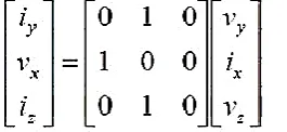
It is a three port device. Three terminals X, Y, Z are used to satisfy all the conditions which CCII needed. Fig2 shows the all conditions which are required for CCII.
Fig 2: Matrix Representation of CCII
Iy = 0, Iz = Ix
IV.CURRENT MIRROR BASED TOPOLOGY
Fig 3: Current mirror based current conveyor [4]
CCII has a mixed translinear loop comprised of two PNP and two NPN transistors. For the positive CCII circuit illustrated in Fig. 3, transistors M1–M4 form the input translinear mixed loop. The current relationship in the loop is characterized by I1I3 = I2I4. The circuit is dc biased by I0, which is proportional to the current flowing through transistor M1 and M3 (Io ≈ I1 = I3). When no load is connected to terminal X, the terminal can be considered as low impedance output port. The input port Y is considered to be the high impedance node.
V. DIFFERENTIAL PAIR BASED TOPOLOGY
Fig 4: Differential pair based current conveyor [3]
The input stage is the important part of second generation current conveyor (CCII) to obtain a large dynamic range. This can be achieved by using N-MOS matched differential pair (MI, M2) and another P-MOS matched differential pair (M5, M6) connected parallel to implement the voltage follower between the X and Y terminals. Transistors (M22, M12) provide the necessary biasing currents for each differential pair separately.
VI. SIMULATION RESULTS
1. NGSPICE Simulation Results of Current Mirror Based Topology
Fig 5: Variation of output voltage as a function of input voltage
Fig 5 shows the relation between the input voltage and output voltage. As per CCII matrix we need Vx=Vy that is satisfied in this graph.
Fig 6: Dynamic Range Representation of Voltage
Fig 7: Current gain according to the frequency
Fig 7 represents the gain of current which will not reduce if we increasebandwidth because current mode circuits do not have the limitation of gain bandwidth product (UGB).
Fig 8: Voltage gain according to the frequency
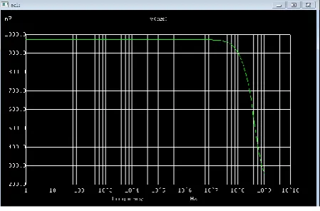
Fig 8 shows the bandwidth of voltage. Current mirror based topology has large voltage bandwidth than differential pair based topology
2. Simulation results of Differential Pair Based Topology
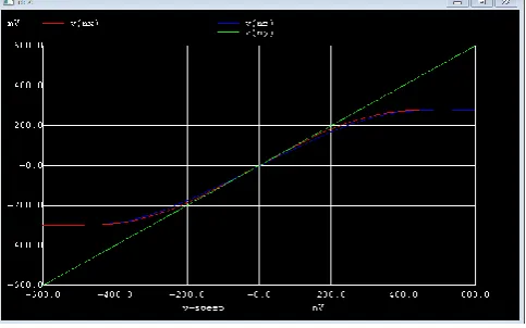
Fig 9 shows the relation between the input voltage and output voltage. As per CCII matrix we need Vx=Vy that is satisfied in this graph. This graph is better than Fig 5.
Fig 10: Voltage gain according to the frequency [3]
Fig 10 shows dynamic representation of voltage in which gives the vdd to -0.6V to +0.6V but get linear response between -0.5V to +0.5V.the problem of non-linearity is overcome using differential pair based topology.
Fig 11: Current gain according to the frequency [3]
Fig 11 represents the gain of current which will not reduce if we increase bandwidth because current mode circuits do not have the limitation of gain bandwidth product (UGB).This topology has higher gain than current mirror based topology.
Fig 12 shows the bandwidth of voltage. Current mirror based topology has large voltage bandwidth than differential pair based topology.
VII.CONCLUSION
The effect of CCII topologies performance is evaluated on the basis of gain, bandwidth and linear characteristics. Bandwidth response for voltage transfer is found to be higher in current mirror based topology than differential pair based topology. But in case of linearity and dynamic range differential pair based topology gives better performance than current mirror based topology. Simulations results are compared for both topologies.
REFERENCES
1. SEDRA, A.S., and SMITH. K.C.: “A second-generation current conveyor and its applications”, IEEE Trans. Circuit Theory,Vol-17, pp. 132-134,1970
2. Sedra, A. S., Gordon W. Roberts, and F. Gohh. "The current conveyor: history, progress and new results." IEEE Proceedings G (Circuits, Devices and Systems) 137.2, pp.78-87, 1990.
3. Ettaghzouti, T., Hassen, N., &Besbes, K. “Novel CMOS second generation current conveyor CCII with rail-to-rail input stage and filter application. In Multi-Conference on Systems”, Signals & Devices (SSD), Vol 11, pp. 1-6, 2014.
4. Ashenafi, E., &Chowdhury, M. H. (2013, December). “Active on-chip voltage regulator based on second generation current conveyor”. In Electronics, Circuits, and Systems (ICECS),Vol 20,pp. 605-608,2013
5. Varshney, G., Pandey, N., Pandey, R., & Bhattacharyya, A. (2013, December). “Performance comparison of filter circuits based on two different current conveyor topologies”. In Signal Processing and Communication (ICSC), International Conference on ,pp. 419-423,2013
6. MazharulHuqChowdhury. "Active on-chip voltage regulator based on second generation current conveyor." Electronics, Circuits, and Systems (ICECS), Vol 20, pp.605-608, 2013.
7. Abolila, Ahmed HM, Hesham FA Hamed, and El-Sayed AM Hasaneen. "New±0.75 V low voltage low power CMOS current conveyor." Microelectronics (ICM), International Conference on. IEEE, pp. 220-223,2010.
8. Varshney, Garima, et al. "Performance comparison of filter circuits based on two different current conveyor topologies." Signal Processing and Communication (ICSC), Conference on. IEEE, pp. 419-423, 2013.
![Fig 4: Differential pair based current conveyor [3]](https://thumb-us.123doks.com/thumbv2/123dok_us/7781936.1285778/3.595.194.396.122.398/fig-differential-pair-based-current-conveyor.webp)
![Fig 12: Variation of output voltage as a function of input voltage [3]](https://thumb-us.123doks.com/thumbv2/123dok_us/7781936.1285778/6.595.167.430.614.759/fig-variation-output-voltage-function-input-voltage.webp)
