ABSTRACT
Koretchko, Kimberly. Solvent Free Post Metal Etch Veil Removal Process Development. (Under the direction of Dr. Jerome J. Cuomo)
As the feature size of advanced integrated circuits decrease, it has become necessary for
the semiconductor industry to start investigating advanced methods of polymer residual removal. When metal lines shrink to 0.25um and beyond, the switching speed of the
device becomes the limiting factor. In order to shrink the dimensions of the metal lines, advanced photo resist technologies such as the use of deep-UV photo resist are used which creates different post metal etch residuals. Residual polymers which are formed
during metal etch processing prove to be more difficult to remove with these advanced photo resists. These residuals, commonly known as veils, become increasingly difficult
to remove with the conventional wet chemical solvent systems. A new technology has emerged that moves away from wet chemical processing. The objective of this
engineering project was to qualify this new technology. The qualification included tool
purchase inputs and development of the new process. The Ulvac Enviro was the tool of choice for this process development. The Enviro provides a unique system which
combines the chemistry of a very low-bias reactive ion etch and remote microwave plasma and fluorine gases resulting in enhancing the solubility of residues in solvents, acids or de-ionized water. The Enviro not only provides a solution to the removal of the
residual polymers it also has a lower cost of ownership and fewer concerns with chemical waste disposal. A two step microwave/RF process was developed using an Enviro. The
process consisted of the following gas flows; NF3, N2/H2(5%) and O2. These gases along
process. A balance between fluorination, oxidation and physical ion bombardment was
developed using the Enviro system. Corrosion, veil removal and metal line profiles were among the main factors that were measured and compared against a standard wet
chemical cleaning process. The experimental work done with this new Enviro process
proved to either match or exceed the existing chemical deveil process. The Enviro process actually showed an improved performance over the standard based on corrosion
results. The Enviro also provided more than a 50% reduction in wafer processing cost, by completely eliminating the need for solvent processing. As a result it was determined that the Ulvac Enviro can provide an excellent alternative to the conventional chemical
Solvent Free Post Metal Etch Veil Removal Process Development
by
Kimberly Koretchko
A thesis submitted to the Graduate Faculty of North Carolina State University
in partial fulfillment of the requirements for the Degree of
Master of Science
MATERIALS SCIENCE AND ENGINEERING
Raleigh 2002
APPROVED BY:
_______________________________ _________________________________
ii
BIOGRAPHY
I received a Bachelor of Science in Materials Science and Engineering from the University of Florida. in 1993. After graduation I began work with Motorola in the semiconductor division as a process engineer in Research Triangle Park, North Carolina.
I began pursuing a Masters of Science in Materials Science and Engineering at North Carolina State University while working at Motorola. I have since transferred with
iii
TABLE OF CONTENTS
Page
LIST OF TABLES………..iv
LIST OF FIGURES……….v
1. INTRODUCTION……….1
2. LITERATURE REVIEW………..3
2.1 Metal Interconnect Processing……….3
2.2 Metal Etch……….………...4
2.3 Post Metal Etch Residues……….6
2.4 Ulvac Enviro II System………8
3. EXPERIMENTAL WORK……….……….11
3.1 Device Summary……….………...11
3.2 In-Line Success Criteria……….13
3.3 Initial Process Development………..16
3.4 In-Line Success Criteria Results………22
4. CONCLUSION………27
5. LIST OF REFERENCES………30
6. APPENDICES……….32
Appendix A Design of experiments ………32
iv
LIST OF TABLES
Page
Table 3.1 In-Line Success Criteria……….13
Table 3.2 NF3/N2/H2(5%) Experimental Runs……….21
Table 3.3 Metal 2 Corrosion Wet Box Testing Results……….22
Table 3.4 Critical Dimension Measurements for Metal 1, 2, and 3………23
Table 3.5 Contamination TXRF Results………27
Table 3.6 Contamination SIMS results………..27
Table A.1 Screening Design of Experiment for Step One………..33
v
LIST OF FIGURES
Page
Figure 2-1 Cross section of backend semiconductor design……….4
Figure 2-2 Metal line post metal etch, with and without resist remaining………6
Figure 2-3 Top down cross section of the Ulvac Enviro II System……….10
Figure 3-1 SEM of metal corrosion post deveil processing………15
Figure 3-2 SEM of metal line with polymer residuals………16
Figure 3-3 SEM of metal line post Enviro and standard deveil processing………..22
Figure 3-4 Enviro oxide loss results………....24
Figure 3-5 SEM of metal 2 profiles……….25
Figure 3-6 Enviro daily particle results………...25
Figure B-1 Parameter of estimates and prediction profiles from NF3 and N2/H2(5%) experiments………...36
1. INTRODUCTION
In fabricating advanced integrated circuits, a multi-level interconnect scheme is
commonly used, and plasma etch is applied to form metal lines and via holes. During the plasma etch, a sidewall polymer or veil is formed to control the etch profile. After the etch, the veil needs to be removed completely to ensure a good via contact resistance and
zero leakage between adjacent metal lines. Typically, a very aggressive amine based chemical solvent is needed to clean up the sidewall polymer because of its heavy metallic
contents.1
As metal interconnect technology moves toward 0.25µm and beyond, it becomes
increasingly important to more thoroughly clean the residues (sidewall polymers and
veils) left behind from the previous processing steps. The metal interconnects of these advance devices become the limiting factor for the switching speed of the device. As a
result, post etch treatment must be recognized as an important step of the process. Some of the issues surrounding new design generations are listed below:
! As dimensions shrink down to 0.4µm, the commonly “allowed” 0.1µm of CD (critical dimension) loss is no longer valid, thus better control of post metal etch corrosion is required.
! The use of more complex material combinations in the process sequence, whether it is for ARC (anti-reflective coating), adhesion layer, eletromigration or stress-relief barrier purposes, creates more complex post etch residues which are still expected to be removed in a minimum number of steps. ! The use of deep UV photo resists which were developed to achieve the
2
sidewall of the features etched are different in constitution and might require specific post etch treatment. 2
With the increasing demands on these devices, new methods of residual polymer or veil
removal are being investigated. One option is a residue solubilization system. This system combines the chemistry of a very low-bias reactive ion etch (RIE) and remote
microwave plasma resulting in enhancing the solubility of residues in solvents, acids or DI water. In some cases this technology is able to completely replace the solvents and acids with simply a post DI water rinse. This technique provides a reduced consumption
of acids and solvents while still meeting the demands for cleanliness on 0.25µm or
smaller devices.
In the semiconductor industry the purchase and qualification of new processes are critical decisions. Tool cost of ownership and process capabilities are essential factors. Several
tool manufacturers are evaluated. Factors that influence cost of ownership include initial cost of the tool, wafer through put, clean room space and mean time between
maintenance. Test wafers are also sent out to tool vendors to provide initial process capabilities. Once a fab commits to a tool vendor and develops a process several millions of dollars are spent to install tools to meet the required wafer capacity needs of the
3 2. LITERATURE REVIEW
In recent years there have been many studies related to veil removal process
development. These studies investigated both solvent free and chemical deveil processes. Many of these studies were used to create the general understanding of the deveil
process. 3-11
2.1 Metal Interconnect Processing
The manufacturing process steps that pertain to the metal interconnect technology and formation of metal lines for connecting devices are the focus of the solvent free strip
procedure. The general procedure consists of depositing a metal film on a wafer, typically less then one micron thick; coating the film with photo resist; exposing the
wafers to ultraviolet light through a mask; developing the resist thereby creating a protective pattern of photo resist on the metal where the metal lines will remain after the metal etch process. Fig 2-1 shows a diagram of the backend metal interconnect
4
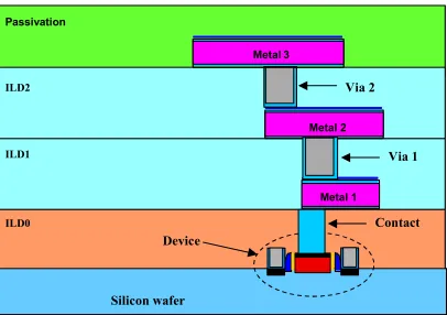
Fig. 2-1. The above diagram is a cross section of a typical backend semiconductor design. Once the device is formed a series of metal interconnects are formed. The first interlayer dielectric (ILD0) is formed using a stack film consisting of TEOS and BPSG. A contact is formed within this IDL0 layer to contact with the device. The ILD0 acts as a barrier layer between the device and the metal layers. The first metal layer is deposited on top of the ILD0 after the contacts are formed. Then another interlayer dielectric is deposited (ILD1). A via is formed within the IDL1 layer to provide contact to metal 1. This process in then repeated and a final passivation film is deposited to protect the device.
2.2 Metal Etch
An adequate metal etch process is required to etch through several different materials (Al and Ti/TiN barrier films) and result in an anisotropic etch with no residue, no corrosion, minimal undercut, good critical dimension control and minimal loss of material
underlying the interconnect materials.12 Typical fluorine-containing gases can not be used for the metal etch process due to the low vapor pressure of the etch by-product,
AlF3, at temperatures below 100°C. Chlorine containing gas such as BCl3, CCl4,SiCl4,
Cl2, are some of the gases used to etch aluminum films. The metal etch process consists
5
of an initial break through step, followed by a bulk Al step. The break through step is
needed to remove the native oxide covering the aluminum and remove any moisture present in the chamber. BCl3 is the preferred source gas for the role of native oxide
removal in many processes. BCl3 is a good getter of oxygen and water vapor, and it
forms heavy ions that are effective in sputtering the native Al oxide. 12
During the main etch step, chlorine is the primary chemical etchant. The ions generated from the BCl3 also act as the source of ions for physical bombardment. An anisotropic
etch is achieved by an inhibiting layer generally referred to as sidewall polymer or veil on
the aluminum surface. It is removed on directional surfaces by ion bombardment; however, the polymer remains on the side wall surfaces of the metal lines creating an
anisotropic etch environment. Fig 2-2 illustrates the sidewall polymer before and after photo resist removal. These inhibiting layers are created from the formation of
chlorocarbon polymers originating from the resist etch by-products. Often additional
carbon containing gases are added to the process in order to enhance the protection of the Al sidewall from undercut. This formation of sidewall polymer becomes a challenge
6
Fig. 2-2. The left diagram illustrates a metal line post metal etch. The film stack consists of underlying TEOS, metal line and resist on top of the metal line. The residue on the sides of the metal line is residual polymer or sidewall polymer created during the previous metal etch. The right diagram illustrates how the metal line and residual polymer appear post O2 ash. The resist has been removed during the ash, however
the sidewall polymer remains.
2.3 Post Metal Etch Residue
Once the wafer has completed metal etch, the next step is to remove the resist and
polymer residue or veil. The first step is to remove the bulk resist from the surface. It is becoming more standard that the bulk resist removal takes places while still under vacuum within the metal etch tool. LAM 9600s and AMAT Metal DPS etchers are
equipped with downstream stripping systems. Most ashers work on the same basic principles: bulk resist removal is achieved by reacting atomic oxygen atoms with the
resist, which basically is a hydrocarbon polymer, to create volatile CO, CO2 and H2O as
the main by-product. 2 Usually the atomic oxygen is created by dissociating oxygen in a microwave plasma or RF plasma. Forming gas which is N2 and H2 is sometimes added to
improve the ash performance and enhance the veil removal. Once the bulk resist is removed, then depending on the prior processing, i.e. metal or via etch, an additional wet
TEOS Resist TiN TEOS TiN TiN AlCu
Side Wall Polymer
Metal line before O
2Ash
Metal line Post O
2Ash
AlCu TiN TEOS Resist TiN TEOS TiN TiN AlCu
Side Wall Polymer
Metal line before O
2Ash
Metal line Post O
2Ash
AlCu
7
chemical clean is required in order to remove the polymers left behind after the resist
strip.
The ash process step is conventionally followed by a wet chemical process which
removes the polymer residues. As mentioned earlier, these residues or veils are generally created during the previous plasma processing in order to create an anisotropic etch
environment. Polymer residues are also created during the previous ash step, known as resist popping. The resist temperature increases too fast and the solvents begin to bubble and pop off the surface of the wafer creating additional by-products on the wafer. Both
of these residues are typically removed using a wet chemical clean process. Although the ash removes the bulk of the photo resist and some of the polymeric materials, a large
amount of residual non-ashed material consisting of metals and complex metal-oxide organic compounds remain. Therefore, the use of solvent post ash processing is required to remove the remaining residues. Common solvents used for this application are
N-methyl-purrolidone (NMP) containing an amine; an organic-aqueous solution containing ethylene glycol, ammonium fluoride, water and a surfactant; or a buffered
hydroxyl-amine solution containing wafer and a chelating agent. 13 These solvents are costly to purchase, hazardous to use and must be disposed of through conventional hazardous waste-handling facilities. For each eight (8) inch wafer processed through a solvent step
typically 0.20-0.40 liters of solvent are consumed. During the solvent process, wafers are first exposed to chemicals to remove the bulk residual for initial cleaning. Then the dirty
8
then go through a series of rinse cycles to remove all remnants of solvents on the wafer
surface. Often this process is done in a spray acid tool; the wafers are placed in a cassette and loaded into a chamber. This chamber rotates or spins the wafers while solvents are sprayed into the chamber. The spinning allows for equal dispersion of the chemicals.
Once the wafers are cleaned, a drying cycle begins which spins the wafers in a nitrogen gas environment in order to dry the cassette and wafers prior to moving on to the next
step.
The industry is now moving towards eliminating the wet chemical clean process with a
microwave/RIE process, followed by a DI water rinse. This dry veil removal has proven to exceed the technical capabilities of the standard wet clean allowing for an increased
process margin and considerable economic cost savings. The Ulvac Enviro is a tool that is capable of removing veil or polymer residue in a solvent free environment.
2.3 Ulvac Enviro System
The Enviro system provides an alternative to the conventional post metal etch wet deveil
process. The Enviro system is an advanced photo resist and polymer removal system which provides solvent free solutions for semiconductor processing. The Enviro deveil system offers more than a 50% reduction in process cost. The lower cost of the Enviro is
attributable to the reduced use of chemicals compared to the conventional wet deveil process. Not only does the Enviro reduce chemical cost it also improves process yield by
9
The Enviro solvent free process benefits from the fact that most of the metallic
compounds incorporated into the polymers or veils are water soluble for example; aluminum chloride, TiCl4 and TiF4. The process maintains a low operating temperature
which prevents oxidation of the metals. At the same time, it is able to ash effectively
rendering the entire remaining material soluble in a simple DI water rinse. 13 A series of plasma chemistry process steps at low temperatures are used for this process. The plasma
chemical treatment includes steps with reactive ion etch (RIE) and remote or downstream microwave plasma treatment, often in combination in order to achieve a dry water soluble residue.
The Enviro consists of the following features14:
! Substantial cost savings over conventional wet processing ! Solvent free processes in production since 1998
! Patented microwave and RIE plasma source in same reactor ! High throughput dual reactor processing
10
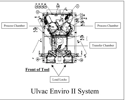
Fig 2-3 The above diagram is a top down cross section of the Ulvac Enviro II System. The front of the tool is bulk head mounted to the operations bay, while the remaining portion of the tool is housed in the gray space (equipment area). The two load locks are accessible through the front of the tool. The transfer chamber houses the robot which transfers the wafers between the load locks and process chambers. Two process chambers are located in the rear of the tool. 14
The tool consists of two (2) processing chambers and two (2) load lock chambers, which
allows for high wafer throughput. The tool can be configured for either a streaming or parallel mode. The “streaming” mode allows the operator to continuously load and
unload wafers from one load lock while continuing to process wafers from the other load lock allowing. This enables maximum tool utilization and an over all lower cost of ownership.
Load Locks
Transfer Chamber Process Chamber Process Chamber
Front of Tool
Ulvac Enviro II System
Load LocksTransfer Chamber Process Chamber Process Chamber
Front of Tool
11
Depending on the length of the process and tool configuration, the Enviro is capable of
obtaining a throughput of up to 50% greater than conventional wet processing. For process flexibility, the Enviro is equipped with both a hot plate and a cold plate. The hot plate allows for wafer processing from room temperature to 300C. These higher
temperature processes are typically used to remove high dose implant photo resist. The cold plate provides processing capabilities from 0 – 90C, this temperature range is typical
for backend applications such as via and metal deveil processes. The Enviro plasma source consists of both a Microwave (2.5kW, 2.45 GHz) and RF (650W, 13.56MHz) capability. The microwave source provides the ability of an increased chemical
environment within the chamber, while the RIE process is more of a physical ion bombardment environment. 14
3. EXPERIMENTAL WORK
The objective of the following experimental work was to develop a dry metal deveil process using the Ulvac Enviro II System. The standard process used a Semitool system
with NOE to chemically remove the veil from the wafers. NOE, which stands for neutral oxide etch, consist of ethylene glycol and ammonium fluoride.
3.1 Device Summary
All experimental work was done on wafers from CDR1 (critical design rules) technology,
12
CDR1 is applicable to new designs intended to be manufactured with the minimum
feature sizes of 0.4 micron. Both logic and nonvolatile memory devices are processed using the CMOS technology. A typical CDR1 device uses three layers of metal, and polysilicon for both the transistors and flash module. The metal layers are each separated
by an inter layer dielectric (ILD). The purpose for the ILD is to decrease capacitance between metal lines and to reduce cross talk between the metal lines. Metal 1 and 2 are
the same thickness, where as metal 3 is thicker.
CDR1 is a planar process which allows for smaller feature size. The planarization
process is done by a chemical mechanical polish procedure. The CDR1 technology also contains unlanded via’s which makes the control of CD’s (critical dimension of metal
line width) more critical.
Metal resistance of the lines is very important. Veil removal or the lack of it can slow the
device down. The resistance becomes very critical for devices that require speed. Also in very tight features, veils can cause leakage from one metal line to the next. Veils can
also cause defectivity issues in the subsequent clean steps, resulting in metal line shorts.
Veil residue can be a source of corrosion. Corrosion is an extremely critical parameter
due to the fact that it becomes a reliability issue. Reliability can be measured by
electromigration testing. The electromigration rule is that if 50% of the Al line is missing
13
1) By-product – Chlorine is still reacting with the metal and leaving by-product. Generally this type of corrosion results in the wafer getting scrapped.
2) Standard corrosion – The corrosion reaction has stopped and there is a void in the metal line. This type is not as serious as by-product. The 50% rule applies to this type of corrosion.
3.2 In-Line Success Criteria
During the development of the metal deveil process, the following in-line success criteria had to be met before committing a product lot to the new process. The objective was to match or exceed Enviro in-line data to the current wet processing in-line data. The
success criteria was defined according to the CDR1 design limits.
Table 3.1
In-Line Success Criteria
Category Spec Procedure
Corrosion defects Zero corrosion defects Wet Box: KLA M2 @ 0.25µm
Veil removal 100% removal of polymer
w/DI rinse only SEM, center and edge
CD Loss +/- 10nm loss CD SEM
Profile Match existing process X-section and top down SEM, center and edge Oxide (TEOS) loss < 250 Å Prometrix, UV1050 or
equivalent TiN Arc loss < 50 Å or match existing
process
Prometrix, SEM
Ti, TiN, TEOS undercut < 100 Å or match existing process
TEM or SEM
Particles < 50 adders of 0.18µm or greater particle size
Tencor 6100 particle analyzer
Contamination Match existing process SIMS/TXRF
14
Test Wafers
The above in-line success criteria was tested using a variety of test wafers. The particle test and contamination testing were completed with bare silicon wafers. All particle measurements were taken using a Tencor 6100 series instrument. Initial particle counts
for particle testing were below 50. Then the wafers were processed through the Enviro on the 2 step deveil process. Wafers were then re-measured on the same Tencor and
particle adders were calculated. The wafers used for contamination testing were virgin wafers that had not seen any processing. A control wafer was tested from the same lot to ensure no incoming contaminates on the wafers.
Oxide loss was measured on test wafers with 16K Å of plasma enhanced TEOS film.
There was no pattern on the oxide test wafers. Resist etch rates were measuring using
1.87µm resist coated wafers. Both of these etch rates were used to monitor the daily tool
performance.
Corrosion defects, veil removal, CD loss, metal profiles and Ti/TiN/TEOS undercut were all tested on short flow test wafers and product wafers. The short flow consisted of 16KÅ underlying TEOS, metal photo pattern, and metal etch. Test wafers were created
for each of the three metal layers. From previous testing it was known that the second metal layer (M2) was most sensitive to the corrosion wet box testing, therefore all
15
Wet Box
A wet box test is an accelerated corrosion test. The wafers are run through a given process (dry deveil), then wafers are immediately placed in a sealed wafer box for 24 hours. The wafer box consists of a wafer cassette and dampened cloths to provide a
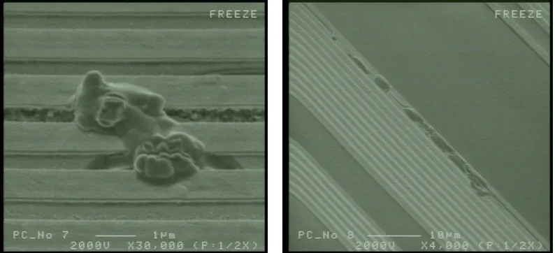
humid environment. If chlorine is still present on the wafers the chlorine will react with the moisture and form hydrochloric acid, which attacks the Al. A control wafer from a known good process was also placed in the wet box to ensure validity of the test. Fig 3-1 represents typical corrosion that might occur post deveil processing if all of the chlorine is not completely removed.
Fig 3-1. Examples of metal corrosion occurring post deveil processing. SEMs were taken after 24 hours wet box test for corrosion.
Veil Removal
The in-line success criteria requires a 100% removal of the polymer post DI rinse. The polymer inspection is done using an in-line SEM. The wafer is inspected top down at about a 30 degree angle at both the center and edges of the wafers. The veil is generally
16
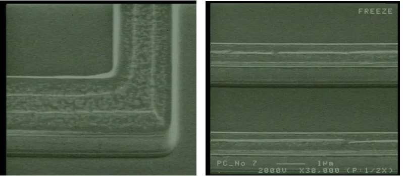
Fig 3-2. Examples of metal lines with polymer residuals post metal etch and O2 ash prior to deveil processing.
3.3 Initial Process Development (Design of Experiment)
The first step towards optimization and development of a process is to determine the important variables using screening experiments. These experiments are designed to
examine a large (greater than 5) number of input factors simultaneously in the same experiment. The objective is to screen out the factors that have a no significant influence on the response within the range of experimentation.
An initial review of all previous dry metal deveil experimental work was completed prior to designing the experiment in an attempt to narrow down the potentially important
variables. Patterned wafers were also sent to Ulvac Technologies for preliminary process development. These test wafers were sectioned into pieces in order to provide multiple
17
was a less aggressive, microwave power based. During this micro step, the majority of
the fluorination of the veils and chlorine exchange occurs. The second step is a more aggressive, power based step used to physically bombard the remaining veil from the top surfaces of the metal lines.
Ulvac Technologies was able to provide a best known method (BKM) process using the
short flow patterned wafers that were sent to them. Using Ulvac’s BKM process, two screening design of experiments were generated. The experiments tested the two step process separately. The first experiment was based around the first micro step while
keeping the second RF step constant at the BKM parameters. The objective was to generate an optimal set of parameters for the micro step. Then a second design of
experiment was run to determine the optimal set points for the RF step. During these experiments, the parameters for the micro step were set to the optimized set points obtained from the initial experiments
Experimental Design
The objective of the initial design of experiment is to determine significant factors from the initial seven factors associated with the first step of the dry metal deveil process. The initial seven factors are as follows:
! Time ! Pin Height
! Microwave power ! Temperature ! NF3
! N2/H2(5%)
18
The responses for the screening experiments are corrosion, oxide loss and veil removal.
Each of these responses have a different level of importance. Corrosion has the most stringent specification therefore, making it the response that is primary concern. Oxide loss and veil removal are of secondary concern, due to wider spec limits.
There are seven factors in the experiment, all of which are continuous. Levels for each
factor were set using the best known method (BKM) as the target values. For each factor, 3 set points were run; target bkm value, 15% above target BKM value and 15% below bkm value. This is the recommended procedure when setting up an initial screening
experiment. It is important to carefully consider the high and low set points because if the levels are too close the interactions may not occur. Similarly, set points are too far
out the experiment may skip over potential interactions.
The experiment assumes 3 factor interactions are negligible. This will be important as
we look at the “confounding structure”. Confounding structure means that there are estimates of how each factor influences response are added together into one number and
can not be separated out in the analysis.
The initial experimental design proposed for the first micro step of the dry metal deveil
process consisted of 35 separate runs. The second RF step experimental design consisted of an additional 16 runs. Once both screening experiments were compete and analyzed,
19
wafers, analytical tool time and personnel. In a manufacturing environment, new process
development is often considered a lower priority; therefore, it was not possible to run the full experimental designed suggested in the above sections. Small portions of the
experiments were run. Trends and interactions were determined from these modified
experiments. Refer to Appendix A for the original design of experiments that were generated for the initial testing of the first and second processing steps.
Trend and Interaction Summary Step 1 (Microwave power step):
The experimentation suggested that the most significant variables in the micro step were interactions between the microwave power, NF3, N2/H2(5%) and O2. The amount of veil
increased as temperature of the chamber was increased. Time and pin height were non-significant variables. In line SEMs results showed a clear improvement of the veil removal as the microwave power increased. However, corrosion wet box testing
indicated high levels of corrosion. An interaction between higher microwave power and increased NF3, N2/H2(5%) and O2 gas flows produced clean and smooth metal line
surfaces and extremely low levels of corrosion. The corrosion levels were monitored post wet box testing. However, it was found that if the O2 flow was too high more oxidation
occurs than fluorination. From these results, a two level full factorial DOE was designed
20 Step 2 (RF power step):
Oxide loss was the main response evaluated while conducting the RF step testing. It was determined that CF4 had no effect on the oxide loss. Higher RF power set points
increased the amount of oxide removed due to the increased amount of ion bombardment.
When process time and RF were increased, the amount of residual visible on the top of the metal lines increased. This was probably attributed to the etching of the TiN surface.
However, if the RF was too low, veil type material was present. It was determined to use the Ulvac bkm for second step of the process and concentrate on the optimization of the microwave step.
Optimization of Microwave Step
Step 1 NF3/N2/H2(5%)Experiment
The goal of this experiment was to determine the optimal flow rates and interaction between NF3 and N2/H2(5%). A 22 full factorial design was created, including one center
point. For both of the factors three set points were run: target, 15% above target and 15% below target. The pattern column in Table 3.2 indicates the set points for each parameter.
21
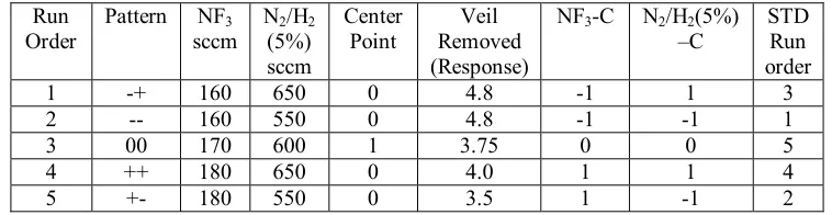
Table 3.2
Ulvac Deveil Experimental runs for Step 1, varying NF3 and N2/H2(5%).
Run Order
Pattern NF3
sccm N2/H2
(5%) sccm Center Point Veil Removed (Response)
NF3-C N2/H2(5%)
–C
STD Run order
1 -+ 160 650 0 4.8 -1 1 3
2 -- 160 550 0 4.8 -1 -1 1
3 00 170 600 1 3.75 0 0 5
4 ++ 180 650 0 4.0 1 1 4
5 +- 180 550 0 3.5 1 -1 2
Veil Removal was the response. The following scale was used to determine the wafer cleanliness (Veil removed response):
1 – No veil removed
2 – Most veil remaining on wafer 3 – Moderate veil removed 4 – Trace amounts of veil present 5 – No veil present
It was determined from the experimental results that NF3 has the largest effect on the veil
removal. Parameter estimate tables and prediction profiles were generated through the use of JMP statistical discovery software. Refer to Appendix B for both parameter
estimate tables and prediction profiles. The results for the experiment indicate that lower NF3 flow produces cleaner wafers. It was also determined that when NF3 flows at a
lower set point, i.e. 160sccm, N2/H2(5%) does not have an effect on veil removal. From
these results it was determined to set the NF3 flow to 160sccm and N2/H2(5%) flow to
22
Fig. 3-3. Both figures are top down SEM pictures. The left SEM was taken post Enviro deveil processing. The right SEM was taken post the standard deveil processing.
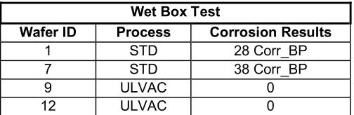
3.4 In-Line Success Criteria Results
All in-line data was collected using the optimized process.
Corrosion
Corrosion (24 hour wet box) testing was completed on the optimized process. Two product wafers from both the standard wet deveil process and experimental dry deveil
process were placed into the same wet box cassette to ensure there was no variability with the wet box procedure. The wafers were tested for corrosion after the metal 2 layer;
previous data has indicated that the metal 2 layer is most sensitive to corrosion.
Table 3.3 Metal 2 Corrosion Wet Box Testing Results Wet Box Test
Wafer ID Process Corrosion Results
1 STD 28 Corr_BP
7 STD 38 Corr_BP
9 ULVAC 0
23
The Enviro results showed no by-product corrosion. Both wafers from the standard
group showed by-product corrosion.
Critical Dimension (CD) Loss
Metal line width post etch and cleans processes is critical in order to maintain device speed requirements. To monitor the metal line width after etch and cleans, a SEM is used
for measurement. Two product wafers from both the standard wet deveil process and experimental Enviro dry deveil process were measured on an in-line SEM for critical dimension (CDs) or metal line width post metal etch. All four wafers were measured
after each metal etch and cleans processing. Table 3.4 gives the critical dimension at each metal layer. M1,M2, and M3 represent the first, second, and third metal layers,
respectively. The success criteria was for the CD average of each metal layer to be within +/- 10nm. There were 9 sites measured on each wafer, the below table is an average of the 9 sites.
Table 3.4 Critical Dimension Measurements for Metal 1,2 and 3
Wafer
ID Process M1 µm CD
M2 CD
µm
M3 CD
µm
03 STD 0.615 0.717 0.708 20 STD 0.609 0.717 0.717
17 ENVIRO 0.613 0.717 0.719
14 ENVIRO 0.611 0.712 0.712
Oxide (TEOS) Loss
Oxide loss was measured on blanket flat film for 30 consecutive days after processing on the Enviro. During this time frame no intrusive chamber maintenance was performed on
24
test wafer with 16K Å of TEOS was pre measured on a Tencor UV1050. Then the oxide
test wafer was run through the Enviro on the optimized deveil process. The test wafer was then post measured on the same UV1050. The oxide loss was calculated from the pre and post measurements.
Fig. 3-4. The amount of oxide loss during a 30 day period on the Enviro system.
Profile (TiN Arc loss and Ti, TiN, TEOS undercut)
The Ulvac profiles match the standard wet deveil process. No significant undercut is
seen on either of the profiles. Fig 3-5 are cross sections that were taken from two production wafers at the end of line. The SEM was taken of the metal 2 line.
Ulvac Dry Deveil Oxide Loss (Å)
160 165 170 175 180 185 190 195 200 205 210 215
1 3 5 7 9 11 13 15 17 19 21 23 25 27 29
Run Number
O
xide Loss (Å
)
25
Fig 3-5 The right figure received the Ulvac deveil processing and the figure on the left received the standard wet deveil processing. SEMs were taken of the second metal stack layer.
Particles
Particles were tested on the tool over a 3 month period. The upper control limit for the
particles is 50 adders for particle sizes 0.18µm or greater. Both the pre and post particle
readings were taken on a Tencor 6100 tool. Figure 3-6 illustrates the particle qualification data results.
Uvlac Enviro Dry Deveil Particle Evaluation
0 10 20 30 40 50 60
1 5 9 13 17 21 25 29 33 37
Particle Qualification Count
Pa
rt
ic
le
Ad
d
O
n
s
Particle Qualification UCL = 50 Adders
26
Particle counts started to increase after 6 weeks of testing. The process chamber was
opened and inspected. We found that the quartzware in the process chamber was beginning to shed particles on the wafers during processing. The quartzware was
replaced and the chamber was wet cleaned. A chamber wet clean involves wiping out the
chamber with DI damped cloths to remove any residual particles in the chamber. Once the maintenance was completed, the chamber was qualified for particles. The particle
counts returned to normal levels. In order to prevent a future particle excursion, we began wet cleaning the process chamber every 15,000 wafer counts. During each wet clean the quartzware was inspected and replaced if it showed signs of degradation.
Contamination
Three wafers were submitted for contamination testing (TXRF and SIMS). The test wafers initially had 1000Å of TEOS on the surface, then were etched back to
approximately 800Å after the Ulvac deveil process. The control wafer was submitted with the initial 1000Å of TEOS and no additional processing.
First the samples were analyzed using Total Reflection X-Ray Fluorescence (TXRF). The instrument used was the TREX 610T, using the tungsten rotating anode X-ray
source. Five sites were analyzed for each wafer. The x,y coordinates for sites analyzed are (0.01,0.01) and (-57,57). These coordinates are given for the wafer oriented notch
down.
27
Table 3.5 TXRF Results
Wafer # pos S Cl K Ca Ti Cr Mn Fe Ni Cu Zn
T35916 #14 cntr 1000 -- -- -- -- -- -- -- -- -- -- EF01DVLA edge 900 -- -- -- -- -- -- -- -- -- --
T35916 #15 cntr 760 -- -- -- -- -- -- -- -- -- --
EF01DVLB edge 680 -- -- -- -- -- -- -- -- -- --
T35916 #13 cntr 630 -- -- -- -- -- -- -- -- -- --
Control, no
process edge 710 -- -- -- -- -- -- -- -- -- -- Detection
limits 19 13 6 6 3 2 1 1 1 1 2
Units are in e10 atoms/cm2 (Area densities)
The 3 samples were then analyzed for alkali metals using the Camera IMS-5f . An oxygen primary beam accelerated to 12.5kV (8keV net impact energy) was used to
sputter the sample. To optimize sensitivity, positive secondary ions were detected. The site analyzed was from the center of the wafers. The SIMs results were all within the
process control limits
Table 3.6 SIMS results
Wafer Description Li Na K
T35916 #14 Processed in EF01DVLA 1e9 2e10 4e9 T35916 #15 Processed in EF01DVLB 9e8 1e10 2e9 T35916 #13 Control, no process <5e7 6e9 <5e7 Units are in atoms/cm2 (Area densities)
4.0 CONCLUSION
28
removal was once considered a non-critical process step, but with the advances in photo
resist and etch processing, veil removal following metal etch has become a challenge to the semiconductor industry. There is a trend toward moving away from the traditional aggressive amine based wet chemical processing to a residual solubilization system
which does not require wet chemical processing. This paper explored one of the many possible solutions for this deveil process conversion.
The Ulvac Enviro system provides a unique system which combines the chemistry of a very low-bias reactive ion etch, a remote microwave plasma and fluorine gases resulting
in enhancing the solubility of residues in solvents, acids or DI water. A two step
microwave/RF process was developed on the Enviro rendering the residual soluble in DI
water. This process was subjected to a series of in-line success criteria and compared with the standard chemical deveil process. Out of all of the input parameters involved in the Enviro process the gases (NF3, N2/H2(5%) and O2), microwave power and RF power
had the greatest impact on the output parameters. By optimizing these conditions a balance between fluorination, oxidation and physical ion bombardment was developed.
For example, as mentioned previously, if the O2 flow was too high more oxidation
occurred rather than fluorination. It was also found that if the RF power was set too high the physical ion bombardment would begin to etch away the TiN surface on the tops of
the metal lines.
29
most critical success criteria. Wet box corrosion testing showed an improvement from
the standard processing. Veil removal, metal line critical dimensions, oxide loss and metal line profile matched the standard deveil process. Overall, the experimental work done with this new Enviro process proved to either match or exceed the existing chemical
deveil processing. Along with processing improvements, the Enviro provided more than a 50% increase in wafer throughput, decreasing the processing cost. However, the
30 5.0 REFERENCES
1. Xu Han, Mohamed Boumerzoug. “Dry Cleaning Technologies for Post Metal and Via Applications”, Symposium on Contamination Free Manufacturing for Semiconductor Processing, Semicon West 1998.
2.Louis D., Lajoinie E. “Addressing Corrosion Issues During Post Metal Etch Treatment”, Future Fab Issue 5 page 1-5, 1998.
3. Bersin, R.L. “Residue-Free Dry Stripping Photo resist Without Solvents or Acids: Time
for a Parading Shift”, Semiconductor FabTech.
4. Boumerzoug Mohamed. “Removal of Titanium Oxide Grown on Titanium Nitride and Reduction of Via Contact Resistance using a Modern Plasma Asher”, Materials Research Society Symp. Proc., Vol 495, page 345, 1998.
5. DeJule Ruth. “Managing Etch and Implant Residue”, Semiconductor International, August, page 56-63, 1997.
6. Hua Li, Baklanow Mikhail, Boullart Werner, Conard Thierry, Brijs Bert, Maex Karen, Froyen Ludo. “Analyses of Post Metal Etch Cleaning in Downstream H2O-Based Plasma Followed by a Wet Chemistry”, Electrochemical Society Vol 146 (10) page 3843-3851, 1999.
7. Joubert O., Pelletier J., Arnal Y. “The etching of polymers in oxygen-based plasmas: A parametric study” Journal of Applied Physics, Vol 65 (12), 15 June, page 5096-5100, 1989.
8. Lau K., Wu W. “Microwave Downstream Plasma Removes Metal Etch Residue”, Semiconductor International, page 231-233, July 1997.
9. Miyaji S., Kato T., Yamauchi T. “Ashing residues on TiN residues on TiN
anti-reflective coating layers”, American Vacuum Society, Vol 14(6), Nov/Dec, page 3082-3085, 1996.
10. Sakuma, Yagi Shoji, Imai Kazuo. “Study of a Veil Structure and a Two-Step
Corrosion Suppression Process in Al-Si-Cu Etching” Journal of Applied Physics, Vol 33 page L617-L619, 1994.
11. Singer, Peter. “Plasma Ashing Moves Into the Mainstream”, Semiconductor International, August 1996.
31
13. Gooch, Michael, Bersin R. “Eliminating Solvents from semiconductor wafer manufacturing”, Extended Abstract, Presented at the 3rd Green Chemistry and Engineering Conference, Washington D.C July 1, 1999.
14. Ulvac Technologies. “The ULVAC EnviroTM Advanced Photo Resist Removal
32 5.0 APPENDICES
Appendix A
The initial screening design of experiment for the micro step was designed with the
following seven factors: time, pin height, microwave power, temperature, and gas flows. For each of the factors three set points were run; target, 15% above target value and 15%
below target value. The pattern column in Table A.1 indicates the set points for each parameter. For each run, the symbols +, -, and 0 stand for 15% above target value, 15% below target value and the target value, respectively. The experimental runs for the
design of experiment were generated using the JMP software, a statistical design
software. The table below lists the experimental runs generated by JMP for the screening
33
Table A.1
Screening design of experiment for step one
Run
Order Pattern NF3 Sccm N2/H2(5%) sccm O2 sccm Pin Height Time sec Temp C MW Power Center Pnt 1 +-+-+-+ 170 425 10350 1 35 40 1725 0 2 ++---+ 170 575 7650 1 25 40 1725 0 3 +-++++- 170 425 10350 3 35 60 1275 0 4 +-++--+ 170 425 10350 3 25 40 1725 0 5 +--++-- 170 425 7650 3 35 40 1275 0 6 ++++--- 170 575 10350 3 25 40 1275 0 7 ---+ 130 425 7650 1 25 40 1725 0 8 0000000 150 500 9000 2 30 50 1500 1 9 -++-+-+ 130 575 10350 1 35 40 1725 0 10 --+-+-- 130 425 10350 1 35 40 1275 0 11 +--+-++ 170 425 7650 3 25 60 1725 0 12 ---+-+- 130 425 7650 3 25 60 1275 0 13 +++-+-- 170 575 10350 1 35 40 1275 0 14 -++--+- 130 575 10350 1 25 60 1275 0 15 -+++--+ 130 575 10350 3 25 40 1725 0 16 ++-++-+ 170 575 7650 3 35 40 1725 0 17 0000000 150 500 9000 2 30 50 1500 0 18 +---+++ 170 425 7650 1 35 60 1725 0 19 -+++++- 130 575 10350 3 35 60 1275 0 20 +-+--+- 170 425 10350 1 25 60 1275 0 21 -+--+++ 130 575 7650 1 35 60 1725 0 22 -+--- 130 575 7650 1 25 40 1275 0 23 -+-+-++ 130 575 7650 3 25 60 1725 0 24 ++-+-+- 170 575 7650 3 25 60 1275 0 25 --+++++ 130 425 10350 3 35 60 1725 0 26 ---++-+ 130 425 7650 3 35 40 1725 0 27 --+--++ 130 425 10350 1 25 60 1725 0 28 +++--++ 170 575 10350 1 25 60 1725 0 29 --++--- 130 425 10350 3 25 40 1275 0 30 0000000 150 500 9000 2 30 50 1500 1 31 ----++- 130 425 7650 1 35 60 1275 0 32 ++++++
+ 170 575 10350 3 35 60 1725 0 33 -+-++-- 130 575 7650 3 35 40 1275 0 34 +--- 170 425 7650 1 25 40 1275 0 35 ++--++- 170 575 7650 1 35 60 1275 0
The initial design of experiment for the second step of the process was set up varying the following factors: time RF power, CF4 and N2/H2(5%). An experiment with sixteen runs
34
Table A.2
Design of experiment for step two
Run Order Pattern CF4 Sccm RF Power watts Time sec N2/H2(5%) sccm Center Pnt 1 -++- 30 290 35 395 0 2 -+-+ 30 290 25 535 0 3 0000 35 250 30 465 1 4 ++-+ 40 290 25 535 0 5 -+-- 30 290 25 395 0 6 ++-- 40 290 25 395 0 7 ---+ 30 210 25 535 0 8 --++ 30 210 35 535 0 9 +-+- 40 210 35 395 0 10 +--+ 40 210 25 535 0 11 +-++ 40 210 35 535 0 12 ---- 30 210 25 395 0 13 --+- 30 210 35 395 0 14 +++- 40 290 35 395 0 15 0000 35 250 30 465 1 16 -+++ 30 290 35 535 0 17 +--- 40 2210 25 395 0 18 ++++ 40 290 35 535 0
As noted earlier, due to the manufacturing environment in which this experimental work
was being conducted in, it was not possible to run both of the experimental designs. However, if the above experimental runs were run, the following steps would have been taken to analyze the result.
Analyze the Results
The following is a 9 step process that can be used to analyze and interpret any fractional factorial screening experiment using the JMP software.
35
2) Create the Model: At this point JMP software is used to fit model. Once the responses have been generated and inputted into the original model, fit model can be generated by using all of the main effects and two-factor interactions.
3) Fit the Model: Examine the tables and graphs, including summary of fit, analysis of variance, lack of fit and parameter estimates.
4) Perform Residual Diagnostics: Create plots of residuals to test assumptions
including: independence of residuals, stability of residuals, equal variance of residuals and normality of residuals.
5) Check for possible transformations: Use the Box-Cox approach. If a transformation is needed it is necessary to go back to the create model step and continue the analysis with the transformed response.
6) Remove non-significant terms/refit the model: Use the parameter estimates table generated in step 3 to remove non-significant terms. Once removed it is important to recreate the model excluding the non-significant terms.
7) Chose the improved model: Once the best model has been chosen, the prediction equation for that model most be saved
8) Interpret chosen model: Use the prediction profile and desirability function to choose an optimal level of input factors. Validate the model results with engineering and scientific knowledge of the process. Then draw conclusions and make
recommendations.
36 Appendix B
Parameter estimate tables and prediction profiles were generated through the use of JMP statistical discover software from the results of the 22 full factorial design that was created for the optimization of the NF3 and N2/H2(5%) gas flows for step one of the
process.
Screening Fit Veil Removal Summary of Fit
RSquare 0.847721
RSquare Adj 0.390884
Root Mean Square Error 0.469574 Mean of Response 4.17 Observations (or Sum Wgts) 5
Parameter Estimates
Term Estimate Std Error t Ratio Prob>|t|
Intercept 4.17 0.21 19.86 0.0320
NF3coded -0.525 0.234787 -2.24 0.2677
N2H2coded 0.125 0.234787 0.53 0.6885
NF3coded*N2H2code 0.125 0.234787 0.53 0.6885
Prediction Profile 4.8 3.5 4.695 1 0 0.919231 NF3coded -1 N2H2coded -1 Desirability
Fig. B-1 The above Parameter of Estimates and Predication Profile was generated with the data created from the NF3 and N2/H2(5%)design of experiment using JMP statistical software.
37
different. However, the prediction profile illustrates that the lower the NF3 flow produces
cleaner wafers. The profile also shows that when NF3 is at the low end, N2/H2(5%) flow
does not have an effect. This is illustrated in the prediction profile below.
Prediction Profile 4.8
3.5 4.695
1
0 0.919231
NF3coded -1
N2H2coded 0
Desirability
Fig. B-2. The above Predication Profile was generated with the data created from the NF3 and
N2/H2(5%)design of experiment using JMP statistical software. The desirability index for each of the
factors was set to give the most optimal response.
The NF3 flow was kept at “–1” set point and N2H2 was moved to the center point. The
desirability number still remains 0.92. It was decided to use NF3 = 160sccm and
N2/H2(5%) = 600sccm flow set point for the remaining in-line testing. We choose the
center point for N2H2 since it did not have an effect on veil removal when NF3 was set to