Available online: https://edupediapublications.org/journals/index.php/IJR/ P a g e | 2665
Low Power Design of Double Ended Bit-lines with Read
Decoupled 8T Static RAM Cell
Devupalli Sunil Kumar
1, Bandi Sarada
2& Manas Ranjan Biswal
31
Student of
M.tech(VLSI),Sanketika Vidya Parishad Engineering College, Affiliated to A.U,
Visakhapatnam, Andhra Pradesh.
2,3
Assistant Professor, Department of ECE, S.V.P Engineering College, Visakhapatnam.
[email protected]
1[email protected]
2Abstract:
To propose a Double ended with read decoupled 8T Static RAM cell, uses the double connectivity of the bit-lines that help in fastly discharging the read data from the stored SRAM cell and improves the cell performance by reducing power consumption and its delay. The proposed cell consumes low power and gives high performance than the existing single ended 8T SRAM-cell.
In this analysis by varying the cell supply voltage and observed the scale down the voltage from 2.2v to 1.2v, maximum power reduction is observed in this proposed cell than existing single ended 8T cell. That is power reduction of proposed cell is significantly reduced to 110.53uw to 316.59nw as compared to the existing cell power reduction is 247.22uw to 704.12nw. At particular cell supply voltage 2.2v, delay time of proposed cell is 35.231ps then existing single ended 8t cell is 25.014ns. the entire design & simulation is implemented in the pyxis tool -130 nanometer scaling CMOS technology.
Application: SRAM have been wide range of applications, used in every memory used display devices for example handheld devices like mobile phones, laptops….etc.,
Keywords:
Single ended 8T-cell, double ended 8T-cell, static random access memory (SRAM) cell, nanometer technology, cell area, delay time and power consumption.
I. Introduction:
The Novel 8-Transistor‟s SRAM cell is logically several types to design by depends on its operational speed and data stability. That means in every portable microprocessor controlled devices contain embedded memory, its occupies a large portion of the system-on chip These portable systems need ultralow power consuming circuits to utilize battery for longer
duration. The power consumption can be minimized using non conventional structures, new circuit topologies. In spite of the fact that, voltage scaling has prompted circuit operation in sub limit administration with least power utilizations.
In this brief, we have outlined another sub threshold double ended 8T SRAM cell that works in sub nanometer innovation hub at ULV. This proposed cell utilizes double finished compose with element criticism slicing to upgrade compose capacity and element read decoupling to dodge read disturb. Because of the double ended cell improves the read operation then conventional 6Tcell. The proposed 8T cell has bigger composed edge as well as has faster composed time. As 8T is double bit line connectors it can spare more power consumption and territory as contrasted. Here, we center mainly on the soundness of the cell which is influenced by the procedure parameter variations. This brief is a detailed dialog of our work on 8T cell, incorporating examinations with other single-finished cells like single ended 8T and 6T cell‟s.
Available online: https://edupediapublications.org/journals/index.php/IJR/ P a g e | 2666
2. Conventional 6T-SRAM Cell:
The Six Transistor SRAM cell is mostly utilized in embedded memory attributable to its quick time interval and relatively little space. The total CMOS 6T SRAM bit cell configuration is shown figure-1.
:
Figure-1. 6T SRAM-CELL Schematic
The 6T SRAM cell consists of two inverters connected back to back. By the N3, N4 access transistors that are controlled by the word line (WL). The cell preserves one in all its two possible states denoted as 0 and 1 as long as power is obtainable to the 6T cell, with help of access transistors like N3 & N4 the data can be either enter or written into the cell. These two cross-coupled inverters are used for storing one bit of information at a time (either 0 or 1) at the storage node like Q & Q.bar.
The 6T-SRAM cell has three different modes. a) Hold Mode (Data into the cell) and
b) Write mode (updating logical data). c) Read mode (data discharge from cell)
These three different Operational modes are classifies as follows.
2.1 Stand-by Mode: (Data hold into the Cell)
In standby mode word line is disabled i.e., WL-1, so that logical data access pass transistors N3 and N4, which is connected to 6t cell at bit lines (two ends of cell) are turned off. It means that cell cannot be allows any logical data into the cell from the bit-lines transfers charges. The two cross coupled inverters formed by P1 + N2(1st inv) & also P2 + N2 (2nd inv)
will continue to feed back each other as long as they are connected to the cell supply like Vdd, while logical data will hold in the SRAM cell.
2.2 Read Mode: (Data Discharge from the cell bit lines)
During read operation, the word line should be enable (WL is high), the WL is enables both the access transistor‟s (N3 & N4). This will connect cell from the bit lines. Then the voltage hike stored in nodes like Q & Qbar, by these BL & BLB ( bit lines). If voltage hike i.e., 1 is stored at node Q so bit line bar(BLB) will discharge through the driver transistor (N4) and the bit line will be pull up through the Load transistors (P1) toward Vdd, a logical 1. The Design of SRAM cell requires read stability. Therefore the data is discharges through the cell by help of the bit line and bit line bar by depend on its data stored (at Q & Q.bar) into the cell.
2.3 Write Mode (Updating logical data):
Available online: https://edupediapublications.org/journals/index.php/IJR/ P a g e | 2667
Figure 2. 6T-SRAM CELL Schematic Design
Figure 3. Layout of 6T SRAM-Cell
3. Existing Single Ended with dynamic Feedback 8T SRAM-Cell:
The single-ended with dynamic feedback control cell is useful to store-to and retrieve-from from the logical data by using single write and read bit-line‟s. The single-ended design is used to reduce the differential switching power during read–write operation. The power consumed during witching of the data on single bit-line is lesser than that on differential
bit-line pair. The cell enables writing through single Nmos (M7) in 8T cell. It also separates the read and writes data exhibits by read decoupling design. The structural change of cell is considered to enhance the immunity against the process voltage variations.
The Single ended 8T-cell has one cross-coupled inverter pair, in which each inverter is made up of three cascaded transistors. These two stacked cross-coupled inverters like M1–M2–M4 (acts as first inverter) and M8– M6–M5 (as second inverter) retain the data during hold mode. The write word line controls only one nMOS transistor like M7, used to transfer the data from single write bit line (WBL). In this cell write operation is done by only activation of the write word line. If write word line is deactivated when no data is allows into the cell because the data access transistor (as M7) is in off mode.
Figure-4. Single Ended 8T SRAM-Cell Structure
Available online: https://edupediapublications.org/journals/index.php/IJR/ P a g e | 2668
respectively. The structure of single ended with dynamic feedback control 8T SRAM Cell as shown in the diagram.
Table-1. Operational Table of Existing Single Ended 8T SRAM-Cell
SINGLE ENDED 8T-CELL OPERATION:
3.1 Write Operation:
In the SRAM-Cell, feedback cutting (Cross coupled Inverter‟s) scheme is used to write into & read from of combination of 8- Transistor‟s SRAM cell.
3.1.1 Writing a “1”:
During write 1 operation FCS1 is made low while the switches transistor M6 in off mode. When the RWL is made low and FCS2 is enabled. Then the FCS2 control transistor M2 will conducts, it is connecting Complementary Q (QB) to the ground. while, the logical voltage data entered to write bit line is 1 (high voltage level) when activated the write word line, then current flows from word bit line to Q(output) and Create the voltage hike on Q via M7 writing high voltage hike i.e., 1 into the 8T-cell. Moreover, when Q changes its state from o to 1, the inverter (M1-M2-M4) changes the state of Q.bar from high voltage hike to low voltage hike (i.e.1to 0). .
3.1.2 Writing a „0‟:
Same as the write-„1‟ operation, to write a „0‟ at Q node, write word line is made enable, FCS2 is made low and write bit line is pulled charge to the ground i.e. 0. The low going FCS-2 leaves Q.bar floating, which can go to a small negative value, and then the current from pull-up Pmos M1 charges Q.bar to high voltage hike i.e., 1 Now, if the data enter to word bit line is „0‟ (low voltage hike) at node Q, when write word line is activated, then the current flows from word bit line to Q (output) and create the voltage hike on Q via dayta access transistor M7 writing
„0‟ then the charges are sharing both Q and Q.bar are by intersect to each other into the 8-Transistor‟s SRAM-Cell.
3.2
Read Operation:
3.2.1 Reading „1‟ from Cell:
The read operation is performed by pre-charging the Read bit line, when the activating RWL. If 1 is stored at node Q then, FCS-2 control transistor M4 is turns ON and makes a low resistive path for the flow of cell current through RBL to ground. This discharges RBL quickly to ground, which can be sensed by the full swing inverter sense amplifier. Since WWL, FCS1, and FCS2 were made low during the read operation therefore, there is no direct disturbance on true storing node QB during reading the cell. The low going FCS2 leaves QB floating, which goes to a negative value then comes back to is original „0‟ value after successful read operation. If Q is high then, the size ratio of M3 and M4 will govern the read current and the voltage difference on Read bit line.
3.2.2 Reading „0‟ from Cell:
During read 0 operation, Q is „0‟ and read bit line has been precharged high value and the inverter sense amplifier gives 0 at output. Since M2 is OFF so virtual QB.bar is isolated from QB and this prevents the chance of disturbance in QB node voltage which ultimately reduces the read failure probability. During read operation, if FCS1/FCS2 turns 1 before read word line are turned 0 then QB and VQB can share charge. As WWL is 0 no strong path exists between WBL and Q, and any disturbance in QB will not affect Q. After that if RWL goes low, the positive feedback will restore the data values with the respective cell nodes Q and Q.bar.
3.3
Control signal Generation:
The feedback control signals (i.e., FCS-1 & FCS-2) are column wise configuration connected to the existing single ended 8T cell. These signals are depends on its performance of the cell input data, that means the SRAM cell input data and column address signals are used to generate these feedback control signals. A common circuit is used fr a single column, therefore, there would e a small area overhead at array level. The existing 8T cell has single ended write and also read port similarly as conventional read decoupled 8T cell.
Lines HOLD W=1 W-0 R-1/0
WWL 0 1 1 0
WBL 1 1 0 1
FCS1 1 0 1 x
FCS2 1 1 0 x
RWL 0 0 0 1
Available online: https://edupediapublications.org/journals/index.php/IJR/ P a g e | 2669
Figure-5. Single Ended 8T SRAM-Cell Schematic Design
Figure-6. Layout of Single Ended 8T-Cell
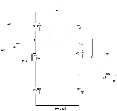
4. Proposed Double Ended with Read
Decoupled 8T SRAM-Cell:
The Double ended 8T-cell is very similar to the conventional 6T-cell & also Existing SRAM cell with an exception of the extra transistors, which are used for read operation. Out of the three extra transistors one transistor (RT-read transistor) is common for the entire row in array formation of SRAM cell array on the SRAM chip.
The double ended 8T cell has one cross coupled inverter pair, in which each inverter is made up
of two cascaded transistor‟s that means the combination of the pmos and nmos process of cmos technology. The back to back connected inverter pairs like P1 and N1 is acts as the first inverter and also other transistor‟s like P2 and N2 is acts as the second inverter, its connectivity as shown in the figure-22. In which the total 8-transistors are used for data enter-to and discharge the data from the cell purposes. The data access transistors as N3 and N4. Which is used to transfer the logical data into cell while activation of write word line and also for read the data purpose used another two buffer transistors like P3 and P4, these two transistors are used to discharge the data bit from the stored sram cell by the activation of the read line or read transistor.
The 8T SRAM cell as shown in figure-7, this structure must to guarantee a nondestructive read operation, NMOS driver transistors N1 and N2 must be size larger than NMOS access transistors N3 and N4, whereas the access transistor‟s are the major fundamental transistors for the write operation. Based on these two transistors, the write operation is performed.
Figure-7: Double Ended with Read Decoupled 8T SRAM-Cell Structure
Available online: https://edupediapublications.org/journals/index.php/IJR/ P a g e | 2670
current does not get affected from radiation. Whereas it increases in NMOS, Moreover, PMOS offers lower flicker noise than NMOS transistor. In addition shallow trench isolation offers compressive stress, which causes degradation in mobility of electron rather than holes near the verge of active region.
In this Double ended 8-Transistor‟s Cell, read and write operation are separate that means These PMOS transistors along with Read transistors decouple the storage nodes while reading. Hence, read operation is improved. In the proposed cell for read and write operation separate bit-lines are used. The double ended cell design is uses RBL (read bit-line) and RBL.bar(read bit line.bar) for read operation and BL(bit line) and BLB(bit-line.bar) for write operation.
Double Ended Read Decoupled 8T
SRAM-Cell Operation:
4.1 Write Operation:
The Write operation of double ended 8T cell is same as the conventional 6T sram cell in which cell consist the one cross coupled inverter pair to store and retrieve data purposes, that means each inverter‟s is designed with combination of pull up and pull down transistor‟s like P1+N1 as first inverter and P2+N2 as second inverter are connected to back to back. These inverters are merged by CMOS technology.
4.1.1 Write „1‟ into Cell:
In this cell write the data into the cell storage nodes, when the write word line is enabled then the data is transferred into the cell by bit line and bit line bar transistors like N3 and N4 that means The bit line has to give a value Vdd and bit line bar is change a value 0 volts by pull down to ground. As write word line is enabled for write operation, the values in bit lines are store at respective nodes that is at Q will have a value logical „1‟ and also logical „0‟ at Q.bar. There is no change in the write operation when compared with the conventional 6T-SRAM cell operation.
4.1.2 Write „0‟ into Cell:
This operation is same as the write –„1‟ operation, During the writing „0‟ into the cell, when at Q has zero volts and Vdd to the bit line (BL.bar) and write word line is enable then makes both the access are transistors N3 and N4 is in active mode. Then the data is enter into the cell by the bitline and bitline bar then the low voltage hike is stored at Q into the cell while
the charges are sharing into the cell then high voltage hike is store at the Q bar. Hence the value in the bit line is stored at Q. Hence low voltage hike i.e „0‟ is stored at Q.
Table-2. Operation Table Of Double Ended 8T SRAM-Cell
4.2. Read Operation:
During read operation both the RBL and RBL.bar are precharged and read line (RL) is turned high. Depending upon the data stored by the storage node either P3 or P4 will conduct. Hence, either RBL or RBLB will discharge through P4 or P3 respectively and finally through RT. Therefore both the storage nodes are not affected during read operation by using separate read bit lines. Thus, cell stability during read operation is improved. That means the voltage value of one of the read bit-lines will be discharged.
4.2.1 Read „0‟ from the cell:
If the storage node Q is holding “0” and Q.bar is holding „1‟. Therefore, PMOS transistor P3 will be on. Therefore, RBL will drop through P3 and read transistor (RT) is asserted that means in this Double ended 8T Cell the read operation is perform, if the read transistor line is ON. Similarly if RT is OFF mode then no read operation is performed.
4.2.2 Read „1‟ from the cell:
During read high voltage hike is same as the read „0‟ operation mode, but in this operation if the Q is holding „1‟ and other inverter have low voltage hike that is Q.bar is „0‟ in this process the pmos transistor‟s like P4 is turns ON then the read bit line bar discharge the high voltage data bit by the activation of the cell array row read line. Hence the discharge the high voltage hike i.e „1‟ at the RBL.bar.
Note: A sense amplifier, if connected between RBL and RBLB will be able to sense and amplifies the voltage hike and finally decipher the stored data.
Line’s W/R-1 HOLD W/R-0
WL 1 0 1
BL 1 1 0
BLB 0 0 1
Q 1 1 0
Qbar 0 0 1
RL 1 0 1
RBL 1 No data Discharge
0
Available online: https://edupediapublications.org/journals/index.php/IJR/ P a g e | 2671 Figure-8. Proposed Double Ended 8T SRAM-Cell
Figure-9. Layout Of Proposed Double Ended 8T-Cell
5. SIMULATION WAVEFORMS:
View the simulation results by selecting the plot results from latest run icon from the left icon palatte of PYXIS tool.
This will open EZ Wave for you with the output waveforms.
5.1 Conventional 6T SRAM-Cell Simulation:
Figure-10. Simulation of 6T SRAM-Cell
Available online: https://edupediapublications.org/journals/index.php/IJR/ P a g e | 2672 Figure-11. Simulation of Single Ended 8T SRAM-Cell
5.3 Proposed Double Ended with Read
Decoupled 8T SRAM-Cell Simulation:
Figure-12. Simulation of Proposed Double Ended with Read Decoupled 8T SRAM-Cell
6. Average Power Measuring:
In the Proposed Double Ended 8-transistors consume less power than the proposed Single Ended 8T that means at particular Vdd (1.8v) the power consume of proposed cell has 707.82nw and the existing single ended cell has 247.22uW.
Similarly, verified the „variation‟ of the power consumption of the SRAM-Cell‟s with respective to „Vdd‟, as shown in the table.
Table-3. Variation of the Vdd vs Avg.Power
7.
Delay-time measuring:
The Performance of the SRAM-Cell was verified by help of operational delay time.
In this delay measuring the proposed Double Ended Read Decoupled SRAM Cell has been less delay than the existing 8T Cell that means at particular Supply voltage at Vdd-1.8v, the delay of existing single ended 8T-Cell has 25.014ns and the proposed 8T-Cell is 92.996ps.
Similarly I verified, „variation‟ of the delay of the SRAM-Cell‟s by variation of different supply voltage of cell.
Table-4. Variation of Delay vs Vdd
Cell Supply voltage
Existing Single Ended
8T-Cell
Proposed Double Ended 8T
Cell
Vdd (V) Consumption Avg.Power Consumption Avg.Power
1.2 704.12nW 316.59nW
1.8 247.22uW 707.82nW
2.2 316.51uW 110.53uW
3.3 546.45uW 144.91uW
Cell Suplly Existing Single Ended
8T-Cell
Proposed Double Ended 8T
-Cell Vdd(V) Delay(ns) Delay(ps)
1.2v 50.048ns 52.706ps
1.8v 25.014ns 92.996ps
2.2v 25.014ns 35.231ps
Available online: https://edupediapublications.org/journals/index.php/IJR/ P a g e | 2673 8. Comparisons of Existing & Proposed 8T
SRAM-Cell‟s:
The proposed Double ended 8T-SRAM Cell no need any feedback control signal as compared to existed Single ended with dynamic feedback controlled 8T-cell. In the Proposed 8T consume less power than the proposed Single Ended 8T-Cell. That mean at particular Vdd (1.8v) the power consume of proposed cell has 707.82nw and the existing single ended cell has 247.22uW.
Similarly the performance of speed of the operation of the SRAM cell is depends on its operational delay time, in which also the performance of the proposed 8T sram cell is high than the existed 8T cell. That means at Vdd-1.8v the delay time of the proposed cell is 92.996ps and the delay time of existed cell is 25.014ns
(Note: 1-nanowatts =10-9 watts, & 1-microwatts =10-6
watts, & 1-picosecond = 10-12)
References:
[i] K.Royand S.Prasad, Low-Power CMOS VLSI Circuit Design, 1sted. NewYork,NY,USA:Wiley 2000.
[ii] Vermaand A.P.Chandrakasan, “A 256 kb 65 nm 8T subthreshold SRAM employing sense-amplifier redundancy,” IEEE J.Solid-State Circuits, vol.43,no.1, pp.141–149,Jan 2000
[iii] C.Kushwah and S.K.Vishvakarma, “Ultra-low power sub-threshold SRAM cell design to improve read static noise margin,” in Progress in VLSI Design and Test
(Lecture-Notes-in-Computer-Science), vol.7373.
Berlin,Germany:SpringerVerlag,2012pp.139– 146.
[iv] B.H.Calhoun and A. P.Chandrakasan, “A 256-kb 65-nm sub-threshold SRAM design for ultra-low-voltage
operation,” IEEE J.Solid-State Circuits, vol.42, no.3, pp.680–688, Mar.2007.
[v] C.B.Kushwah, D.Dwivedi, and N.Sathisha, “8T based SRAM cell and related method,” U.S.
[vi] J.P. Kulkarni, K.Kim, and K.Roy, “A 160 mV robust Schmitt trigger based subthreshold SRAM,” IEEE J.Solid-State Circuits, vol.42, no 10, pp.2303–2313, Oct.2007.
[vii] C.H.Lo and S.Y. Huang, “P-P-N based 10T SRAM cell for lowleakage and resilient sub-threshold operation,” IEEE J.Solid-State Circuits, vol.46, no.3, pp.695–704, Mar.2011.
[viii] I.Carlson, S.Andersson, S.Natarajan, and A.Alvandpour, “A high density, low leakage, 5T SRAM for embedded caches,” in Proc.30th Eur.Solid-State Circuits Conf., Sep.2004, pp.215– 218.
[ix] B.Zhai, S.Hanson, D. Blaauw, and D. Sylvester, “A variation-tolerant sub-200 mV 6-T subthreshold SRAM,” IEEE J. Solid-State Circuits, vol.43, no.10, pp.2338–2348, Oct.2008.
[x] Design and Analysis of an 8T Read Decoupled Dual Port SRAM Cell for Low Power High Speed Applications. International Journal of Electrical, Computer, Energetic, Electronic and Communication Engineering Vol:8, No:4, 2014.
[xi] T. Suzuki, H. Yamauchi, Y. Yamagami, K. Satomi, and H.
Akamatsu, ―A stable 2-port SRAM cell design against
simultaneously read/write disturbed accesses,‖ IEEE J. Solid -State Circuits, vol. 43, no. 9, pp. 2109–2119, Sep. 2008
[xii] H. Noguchi, S. Okumura, Y. Iguchi, H. Fujiwara, Y. Morita, K.
Nii, H. Kawaguchi, and M. Yoshimoto, ―Which is the best dual
-port SRAM 8T, 10T single end, and 10T differential,‖ in Proc. IEEE
Int. Conf. Integr. Circuit Design Technol., Jun. 2008, pp. 55–58.
[xiii] Chang L.etal. An 8T SRAM for variability tolerance and low-voltageopert. in High-performance caches. Solid-state circuits, IEEE journal of 2008; 43(4): 956-963.
[xiv] M.-H.Tu, J.-Y.Lin, M.-C.Tsai, S. J.Jou, and C.-T Chuang,
“single ended Subthreshold SRAM with asymmetrical write and
read-assist,” IEEE Trans. Circuits syst. I, Reg. Papers, Vol.57,