HIGH SPEED SHARING LOGIC BIST
ENVIRONMENT CREATION FOR TESTING
OPERATION
K. Satya Manuja, Elec tronic s and Communic ation Engineering
ABSTRACT – When built-in test generation used for a design that can be partitioned into logic
blocks, it is advantageous to identify groups of blocks whose tests have similar characteristics, and use the same
built-in test generation logic for the blocks in each group. This project studies this issue for a built -in test
generation method that produces functional broadside effects. Functional broadside effects are important for
addressing over testing of delay faults as well as avoiding excess power dissipation during test application. The
project discusses the design of the test generation logic for a group of logic blocks, and the selection of the groups.
Functional broadside tests are two-pattern scan based test that avoid over testing by ensuring that a circuit
traverses only reachable states during the functional clock cycles of test. In addition, the power dissipation during
the fast functional clock cycles of functional broadside tests does not exceed that possible during functional
°operation. Onchip test generation has the added advantage that it reduces test data volume and facilitates at
-speed test application. This project shows that on -chip generation of functional broadside tests can be done using
a simple and fixed hardware structure, with a small number of parameters that need to be tailored to a given
circuit, and can achieve high transition fault coverage for testable circuits. With the proposed on chip test
generation method, the circle is used for generating reachable states during test application
.I.INTRODUCTION
Over testing due to the application of two-pattern scan-based tests was described. Over testing is related to the detection of delay faults under non-functional operation conditions. When an arbitrary state is used as a scan-in state, a two-pattern test can take the circuit through state-transitions that cannot occur during functional operation. As a result, slow paths that cannot be sensitized during functional operation may cause the circuit to fail. In addition, current demands that are higher than those possible during functional operation may cause voltage drops that will slow the circuit and cause it to fail. In both cases, the circuit will operate correctly during functional operation.
Functional broadside tests assure that the scan-in state is a state that the circuit can enter during functional operation, or a reachable state. As broadside tests, they operate the circuit in functional mode for two dock cycles after an initial state is scanned in. This results in the application of a two-pattern test. Since the scan-in state is a reachable state, the circuit goes through state-transitions that are guaranteed to be possible during functional operation. Delay faults that ate detected by the test an also affect functional operation. This alleviates the type of over testing described Test generation procedures for functional and pseudo-functional scan-based tests were described in. The procedures generate test sets for application from an external tester Functional scan-based tests use only
reachable states as in states, pseudo-functional scan-based tests use functional constraints to avoid unreachable states that are captured by the constraints. This work considers the on-chip (or built-in) generation of functional broadside tests. On-chip test
generation reduces the test data volume and facilitates at-speed test application. On chip test generation methods for delay faults, such as the ones described do not impose any constraints
on the states used as scan-in states Experimental results indicate that an arbitrary state used as a scan-in state is unlikely to be a reachable state. The on-chip test
generation method form applies pseudo-functional scan-based tests. Experimental results indicate that pseudo-functional tests are not sufficient for avoiding unreachable states as scan-in states. The on-chip test gen-ration process described in this work guarantees that only reachable states will be used.
Under the proposed on-chip test generation method, the circuit is used for generating reachable states durin g test application. This alleviates the need to compute reach-able states or functional constraints by an off-line process. The underlying observation is related to one of the methods used for external test generation, and is the following. If a primary input sequence A is applied in functional mode starting from a reachable state, all the states traversed under A are reach-able states. Any one of these states can be used for the application of a functional broadside test. By generating A on-chip and ensuring that it takes the circuit through a varied set of states, the on-chip test generation process is able to achieve high transition fault coverage using functional broadside tests based on A.
The paper is organized as follows. It gives an overview of the on-chip geo-ration and application of functional broadside tests and describes the details. It presents experimental results demonstrating the achievable fault coverage
II.BLILT-IN TEST GENERATION
The built-in test generation method from brings the circuit into reachable states by initializing the circuit into a state denoted by Sin it, which is the initial state of the circuit for functional operation, and applying a primary input sequence A of a fixed length, L, in functional mode.
Let A=a(0)a(1)…….a(L-1),where a(u) is the primary input vector at clock cycle u, for 0 <=u < L. Suppose that application of A takes the circuit through the sequence of states S(0)s(1)s(2) ……s(I), where s(0)=Sin it. For 0 <= u < L,s(u+1) is the next-state obtained when the circuit is in present state sõup and the I primary input vector a(u) is applied.
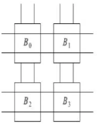
Fig 1: Example of Logical Blocks
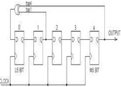
The primary input sequence A is generated by an LF SR whose states are used as pseudo-random vectors. The LFSR sequence is modified in order to avoid an effect called repeated synchronization, where certain primary input values cause certain state variables to assume the same values repeatedly.
The logic for generating the primary input sequence A is illustrated by Fig. 2. For a parameter denoted by d, a distinct set of d bits of the LFSR is used for determining the sequence applied to every primary input. For a parameter denoted by mod, up to mod of the d bits dedicated to each primary input are used for avoiding repeated synchronization.
If the value 0 on a primary input synch ro nizes fewer state variab les than the value I. then the value 0 is preferred. In this case. a mod-input AND gate is used for ensuring that a 0 appears more often than a 1 on this primary input. A mod-input OR gate is used for the primary input if the value 1 synchronizes fewer state variables, and it is thus the preferr ed value for the primary input. No gate is used if both values synchronize the same number of state stables. For a circuit with n primary inputs, this method requires an LF SR with d n bits, and at most one mod-input gate for every primary input. The preferred values of the primary inputs are captured in a primary. input cube denoted by c. For a primary input j, c(j) indicates its value, which maybe 0, 1
.
Fig 2: Test Generation Logic
Several primary input sequences are applied by using several different seeds for initializing the LS SR. Each additional sequence results in a different set of functional broadside tests, and helps increase the fault coverage. All the sequences use the same values of the parameters L, d and mod. Consequently, the same logic is used for generating all the tests.
equal lengths. This can be achieved by adding dummy flip flops to the shorter scan chains.
2.1 BIST Architecture:
A typical BIST architecture consists of • TPG - Test Pattern Generator • TRA — Test Response Analyzer • Control Unit
As shown in figure below
It generates test pattern for CUT. It will be dedicated circuit or a micro processor. Pattern generated may be pseudo random numbers or deterministic sequence. Here we are using a Linear Feedback Shift Register for generating random number. The Architecture for LFSR is as shoat below.
Fig 4: The Architecture for LFSR
Tapping can be taken as we wish but as per taping change the LFSR output generate will change & as we change in no of flip-flop the probability of repetition of random number will reduce. The initial value loading to the LFSR is known as seed value.
2.2 Test Response Analyzer (TRA):
TRA will check the output of MISR & verify with the input of LFSR & give the result as error or not.
2.3 BIST Control Unit:
Control unit is used to control all the operations. Mainly control unit will do configuration of CUT in test mode/Normal mode, feed seed value to LFSR, Control MISR & TRA. It will generate interrupt if an error occurs. You can cleat interrupt by interrupt clear _i. signal
2.4 Circuit under Test (CLT):
CUT is the circuit or chip in which we ate mine to apply BET for testing stuck at zero or murk at one error. Need for using BIST technique
Today’s highly integrated multi-layer boards with fine-pitch ICs are virtually impossible to be accessed physically for testing. Traditional board methods which include functional test only accesses the board’s primary I/Os providing limited coverage and poor diagnostics for board network fault. In circuit testing, another traditional test method works by physically accessing each wire on the board via costly “bed of nails” probes and testers. To identify reliable testing methods which will reduce the cost of test equipment, a research to verify each VLSI testing problems has been conducted. The major problems detected so far are as follows:
• Test generation problems • Gate to I/O pin ratio Test Generation Problems
The large number of gates in VLSI circuits has pushed computer automatic-test-generation times to weeks or months of computation. The numbers of test patterns are becoming too large to be handled by an external tester and this has resulted in high computation costs and has outstripped reasonable available time for production testing.
• The Gate to I/0 Pin Ratio Problem
As ICs grow in gate counts, it is no longer true that most gate nodes are directly accessible by one of the pins on the package. This makes testing of internal nodes more difficult as they could neither no longer be easily controlled by signal from an input pin (controllability) nor easily observed at an output pin (observe ability). Pin counts go at a much slower rate than gate counts, which worsens the controllability and observe ability of internal gate nodes
III.PROPOSED SYSTEM DESIGN 3.1 Low Power Pattern Generation:
intermediate vectors are minimal at best consisting of few logic gates.
The number of LFSR outputs required is driven by the number of test inputs required for circuit under test
The technique of insetting 3 intermediate vectors is achieved by modifying the conventional LFSR circuit with two additional levels of logic between the conventional flip-flop outputs and the low power outputs as shown in Figure 2.10. The first level of hierarchy from the top down includes logic circuit design for propagating either the present or the net state of the flip-flops to the second level of hierarchy. The second level of hierarchy is a multiplexer function that provides for selecting between the two states (present or next) to be propagated to the outputs as low power output at best consisting of few logic gates.
FIG 6: LP-LFSR
In the simulation environment, the outputs of the flip-flops are loaded with the seed vector. The feedback tape are selected pertinent to the characteristic polynomial x + x + 1. Only 2 inputs pins, namely test enable and clock are required to activate the generation of the pattern as well as simulation of the design circuit. It is also noteworthy here that the intermediate vectors in addition to aiding in reducing the number of transitions can also empirically assist in detecting faults just as good as the conventional LFSR pasterns description of the technique to produce low power pattern for BIST. The following is a description of a low test pattern generation technique as depicted in the 9-bit LFSR based schematic in Figure 4.1. Verilog based test bench as shown in Appendix B is used in assigning the initial output states (0100 1011) of the 9-bit LFSR. The feedback taps are designed for maximal length LFSR generating all zeros and all one's as well.
The first step is to generate T1, the first vector by enabling (clocking) the first 4-bits of the LFSR and disabling (not clocking) the last 4 bits. This Shifts the first 4 bits to the right by one bit. The feedback bits of the LFSR are the outputs of the 8th and the first flip-flop. The output of the 8th flip-flop is 1 and the output of the first flip-flop is O. The exclusive-or of the 8th flip-flop (logic 1 in this case) and the first flip-flop (logic 0 in this case) is input (1 EXOR 0 = 1 into the first D flip-flop. The new pattern in the first four bits of the LFSR is 1010. Note that the shaded register is clocked along with the first 4 bits of the LFSR. So the input of the shaded flip-flop is the output of the 4th flip-flop which in this case is O. Also note that prior to the first clock, the input of the shaded register was the seed value of the 4th flip-flop at the output of the 4th flip-flop which in this case is 0. So after the first clock this value of 0 will now appear at the output of the shaded flip-flop. In other words the value, of the 4th output is stored in this shaded register and is used in the next few steps. The first 4 shifted bits of the LFSR and the last 4 un-shifted bits (i.e. the seed value) are propagated as T1 (1010 1011) to the final outputs. Next few steps involve generating the 3 intermediate patterns from T1. These patterns are defined as Ta, Tb and Tc shown in below flow.
Fig.7: Proposed Algorithm for low power LFSR
from T1) as the final first four low power outputs 1010. Note that the clock to the last four bits of the LFSR is also disabled.
The last four bits however are the outputs from the injector circuits. The injector circuit compares the next value (the input of the D-flip-flop) with the current value (the output of the D-flip-flop). According to T1, the outputs (current values) of the last 4 bits of the LFSR are 1011.The next values are the values at the inputs of the D-flip-flops which in this case are 0101. Compare the current values (1011) bit by bit with the next values (0101). If the values bit by bit are not the same then use the random generator feedback R (in this case is logic I) as the bit value as shown in the schematic above. If however both values bit by bit are the same then propagate that bit value to output at opposed to the R bit. This bit by bit comparison gives us the last four bits of Ta to be 1111. Therefore Ta = 1010 1111. Next step is to generate Tb. Shift the last 4 flip-flops to the right one bit but do not shift the first 4 flip-flops to the right. The clock to the first 4 bits plus the shaded flip flop is disabled. The clock to the last 4 bits is enabled. Propagate the outputs of the flip-flops of the entire LFSR at opposed to the outputs of the injection circuit to the outputs (low power). The injection circuits are disabled. As in Ta, maintain the first four LFSR outputs (1010) at the low power outputs. Again from Ta,
the inputs of the last four D flip-flops from the previous step (generating Ta) are 0101. Also note that the output of the shaded register is 0 from the previous step (generating Ta). Therefore the input of the 5th flip-flop is a 0. The outputs of the last 4 flip-flops are 0101 resulting in Tb = 1010 0101. The 3rd intermediate vector Tc is generated via disabling the clock to the entire LFSR. Propagate the first 4 outputs from the injection circuit at the first 4 low power outputs and maintain the last 4 low power outputs the same at Tb. Generating injection circuit outputs for Tc is conceptually the same as explained above in generating Ta. Current values (the outputs of the flip-flops) of the first four flip-flops are compared with the next values (the inputs of the flip-flops) of the flip-flops. The feedback from the 8th flip-flop is 1 (please see generating Tb). Therefore the logical feed forward value of R is 1. The feedback value from the first flip-flop is also 1 as per the current values above. The exclusive are of two ones is a 0. Therefore the input to the first flip-flop is a 0 which is also the next state of the first flip-flop. Hence the next values are 0 for the
first flip-flop and 101 for the 2nd , 3rd and 4th flip-flop respectively. The next values are 0101. The first four outputs from the injection circuit are 1111. The last 4 outputs are the same at Tb which are 0101 resulting in the 3rd and final intermediate vector Tc = 1111 0101. Generating T2 is quite similar to generating T1. As in Tc the outputs of the last four LFSR flops are 0101. The outputs of the first 4 flip-flops of the LFSR are the current values which are 1010. Therefore the seed vector for generating T2 is 1010 0101. Shift the first four bits of the LFSR plus the shaded flip-flop. Do not clock the last four flip-flops. Propagate the outputs of the entire LFSR to the final low power outputs. The
output of the 8th flip-flop from the previous step (generating Tc) is a 1 and the output of the first flip-flop from the previous step (generating Tc) is also a 1. The exclusive or of the output of the 8th flip-flop and the first flip-flop is 0. Therefore the input to the first flip-flop will be a 0. The inputs to the 2nd, 3rd, 4th and the shaded flip-flops are 1010. These are also the current values from the previous step (generating Tcs). Shifting the first four flip-flops of the LFSR to the right by one bit, results in 0101 as the outputs of the first four flip-flops. Therefore T2 generated is 0101 0101.
3.2 Groups of Logic Blocks:
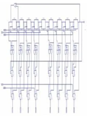
This section considers the built-in generation of functional broad-side tests for groups of logic blocks. The section starts with a discussion of the case where a group G is given. It then considers the selection of groups, and the identification of subsets of seeds for the individual blocks in a group.
Fig 8: Test generation logic for group
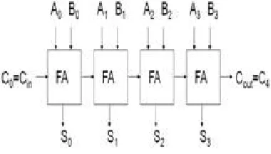
3.3. Ripple Carry Adder.
Ripple carry adder is an n-bit adder built from full alders. Fig 2.1 shows a 4-bit ripple carry adder. One full adder is responsible for the addition of two binary digits at any stage of the ripple carry. The carryout of one stage is fed directly to the carry-in of the next stage. Even though this is a simple adder and can be used to add unrestricted bit length numbers, it is however not very efficient when large bit numbers are used
Fig 9: 4b Ripple Carry Adder
least significant bit to the most significant bit ,which is approximated by:
T = (n-1) tc + ts
IV. RESULTS
Schematic view:
RTL Schematic View
Wave form:
CONCLUSION
The paper studied the built-in generation of functional broadside tests for a design that can be partitioned into logic blocks. In this ass, it is advantageous to use the same built-in test generation logic for groups of blocks whose tests have similar characteristics. This implies using the sane LFSR, with the same AND and OR gates, and the same seeds, for all the logic blocks in the group. The paper described a procedure for constructing the groups. Considering the set of seeds computed for a group, the paper also identified subsets of seeds that are required for every logic block individually. This is useful for testing a subgroup, for example, if power considerations require smaller groups of logic blocks to be tested simultaneously, or if some of the logic blocks are disabled due to faults that were detected earlier.
REFERENCES
[1] J.Rearick. “Too much delay fault coverage is a bad thing,” in Proc.Int Test Conf, 2001,pp_624-633. [2] J.Saxena, K. M. Butler, V. B. Jayaram, S. Kundu, N. V. Aravind, P.SreePakash, and M. Hachinger,”A case study of IR-drop in structured at speed testing,” in Proc. Int test Conf, 2003,pp.1098-1104.
[3] S.Sde-Pax and E. Salomon, “Frequency and power correlation between speed, scan and functional tests,” in Proc .Int Test Conf, 2008.pp,1-9, Paper133.
[4] L.Pomeranx and S.M. Reddy, “Generation of functional broadside tests for transition faults,”IEEE Trans.Comput-Aided Design Integr, Circuits Syst, vol 25,no.10,pp.2207-2218, Oct 2006.
[5] J.Savir and S.Patil, “Broad-side delay test,” IEEE Trans, Comput-Aided, Design Integr Circuits Syst, vol 13, no 8,pp 1057-1064, Aug 1994.
[6]L.Pomeranx,”On the generation of scan-based test sets with reachable states for testing under functional operation conditions,” in Proc. Design Antom, Conf,2004,pp. 928-933.
[7] Y.C. Lin. F-Lu. K.Yang and K.T. Cheng, ”Constraint extraction for pseudo-functional scan-based delay testing,” in Proc. Asia South Pacific Design Antom. Conf, 2005, pp. 166-171.
[8] M.E.Amyeen, A. Jayalakshmi, S. Venkataraman, S.V.Pathy and E.C.Taan,”Logic BIST Silicon Debug and volume Diagnosis Methodology,”Proc. Int. Test Conf., pp. 1-10,2011.
[9] M.Abramovici, M.A.Brener and A.D.Friedman, “Digital systems Testing and Testable Design” IEEE Press, 1995.