R E S E A R C H
Open Access
Unified transform architecture for AVC, AVS,
VC-1 and HEVC high-performance codecs
Tiago Dias
1,2,3*, Nuno Roma
1,2and Leonel Sousa
1,2Abstract
A unified architecture for fast and efficient computation of the set of two-dimensional (2-D) transforms adopted by the most recent state-of-the-art digital video standards is presented in this paper. Contrasting to other designs with similar functionality, the presented architecture is supported on a scalable, modular and completely configurable processing structure. This flexible structure not only allows to easily reconfigure the architecture to support different transform kernels, but it also permits its resizing to efficiently support transforms of different orders (e.g. order-4, order-8, order-16 and order-32). Consequently, not only is it highly suitable to realize high-performance multi-standard transform cores, but it also offers highly efficient implementations of specialized processing structures addressing only a reduced subset of transforms that are used by a specific video standard. The experimental results that were
obtained by prototyping several configurations of this processing structure in a Xilinx Virtex-7 FPGA show the superior performance and hardware efficiency levels provided by the proposed unified architecture for the implementation of transform cores for the Advanced Video Coding (AVC), Audio Video coding Standard (AVS), VC-1 and High Efficiency Video Coding (HEVC) standards. In addition, such results also demonstrate the ability of this processing structure to realize multi-standard transform cores supporting all the standards mentioned above and that are capable of processing the 8k Ultra High Definition Television (UHDTV) video format (7,680×4,320 at 30 fps) in real time.
Keywords: Video coding; Multi-standard; Transform architecture; Systolic array; FPGA
1 Introduction
Multimedia centric devices and applications, especially those based on digital video, have become increasingly popular along the past decade as a result of the latest technological advances. Examples of such systems include video surveillance, IPTV and high definition (HD) TV equipment, as well as the most recent mobile and portable devices, which already offer high-quality video telephony and video conferencing services. Despite their quite dis-tinct characteristics in terms of performance, memory capacity, communication bandwidth and power consump-tion, nowadays, most of these systems must be capable of processing not only standard definition (SD) contents but also the much more computationally demanding HD con-tents. Furthermore, they are also required to support sev-eral different state-of-the-art video standards, including
*Correspondence: [email protected]
1INESC-ID, Rua Alves Redol, 9, Lisbon 1000-029, Portugal
2IST, Universidade de Lisboa, Avenida Rovisco Pais, 1, Lisbon 1049-001, Portugal
Full list of author information is available at the end of the article
the MPEG-4 Advanced Video Coding (AVC)/H.264 [1], the Audio Video coding Standard (AVS) [2], the VC-1 [3] and the High Efficiency Video Coding (HEVC)/H.265 [4] standards, due to interoperability issues and to guaran-tee their commercial success. Consequently, video codecs based on highly specialized hardware processing struc-tures have become fundamental building blocks of mul-timedia systems in several application domains, so as to make them able to efficiently support the encoding and the decoding of a diverse set of contents in real time.
Despite the several existing differences in the adopted coding algorithms, almost all the state-of-the-art video standards implement the classical block-based motion-compensated transform coding scheme [5] and try to maximize the offered compression efficiency for a given video quality. Data compression is mostly achieved in the spatial domain by the transform and quantization stages of the codec, where transforms are used to decor-relate the residual data and compact its energy at the low-frequency domain. In practice, most of the achieved
data compression is provided by the quantization mod-ule, which efficiently exploits the reduced sensibility of the human visual system to higher frequency contents, by adaptively coding the obtained transform coefficients.
Nevertheless, transform coding has been an active research topic for several decades, due to the signifi-cant impact of this operation in the achieved compression efficiency. This investigation has addressed not only the definition of new transforms to be included in novel video standards but also the design of efficient algorithms and circuits for their computation. As a result, various trans-forms with distinct sizes and kernels have been presented in the literature, although the majority of such proposals are based on the type II order-8 discrete cosine transform (DCT) [6]. This is owed to the reduced complexity and the highly satisfactory performance of the DCT in terms of energy compaction, as well as to the existence of fast algorithms for its computation [6].
Nevertheless, transforms of different orders (i.e. order-2, order-4, order-16 and order-32) are nowadays also considered by the most recent video standards (e.g. AVC, AVS, VC-1 and HEVC), in order to improve the cod-ing efficiency, both for HD videos and for low-complexity mobility applications. These smaller transforms are more suitable to process the smaller block sizes resulting from the application of enhanced Inter and Intra prediction techniques in the encoding of low-resolution videos, since they allow to improve the energy compaction and reduce the quantization error. Conversely, larger transforms allow to greatly increase the compression rate for HD contents. However, this higher compression efficiency also comes at the expense of increased computational complexity and required data processing performance. This poses sev-eral challenges to codec and system designers, especially when real-time operation is demanded. This issue is even more problematic for the newest multimedia devices, which are required to support several different video stan-dards. In fact, to implement the several different video codecs, they must efficiently compute the corresponding set of two-dimensional (2-D) transforms. Consequently, the investigation of high-performance and area-efficient multi-standard transform (MST) architectures is nowa-days a very active research area.
In this paper, a unified architecture is proposed for the implementation of high-performance MST cores. The proposed scalable and configurable hardware structure is based on a 2-D systolic array transform core, which was recently proposed for the computation of the transforms adopted in the AVC and HEVC standards [7]. Such trans-form core presents a modular and flexible interconnection architecture that not only allows it to be reconfigured to support different transform kernels but also permits its rescaling to efficiently support transforms of multi-ple sizes. In this work, such properties are extensively
exploited to propose individual transform cores for the AVC, AVS, VC-1 and HEVC standards. Moreover, a MST core capable of processing the transforms defined in all these standards in a single hardware structure is also presented. To achieve such goal, several new pro-cessing elements (PEs) with both dedicated and multi-standard computation capabilities are also introduced herein.
The rest of this paper is organized as follows. Section 2 provides a review of the set of transforms adopted in the previously mentioned video standards, while the most rel-evant related work is introduced in Section 3. Section 4 presents the proposed MST architecture, as well as the set of PEs that are used to compute the AVC, AVS, VC-1 and HEVC transforms. The experimental results considering the implementation of these PEs and of a MST transform core in a Xilinx Virtex-7 FPGA device are presented and discussed in Section 5, by considering other state-of-the-art designs with similar functionalities. Finally, Section 6 concludes the presentation.
2 Transform coding
The type II DCT [6] has been extensively used in block-based image and video coding, such as in the JPEG, H.261/3 and MPEG-1/2/4 standards. This is mainly a consequence of its modest complexity and robust approx-imation to the statistically optimal Karhunen-Loève trans-form [5], which allows to obtain implementations with good performance, both in terms of computation time and energy compaction.
since they make an extensive use of prediction tech-niques to increase their compression efficiency [1-4], thus becoming particularly sensitive to the prediction drift.
To circumvent this problem, state-of-the-art video stan-dards have adopted integer transforms with almost the same symmetry and energy compaction capability than the DCT. Although several different approaches can be used to obtain such transform kernels, dyadic symmetry schemes [8] have been followed in almost all the stan-dards. This approach not only allows to compute the transform in reduced bit-width integer arithmetic (e.g. 16 bits) but also exclusively using integer multiplications and additions. However, since the basis vectors of these inte-ger transforms do not have the same norm, this approach often implies an additional normalization stage in the video coding algorithm. In many video standards, this compensation has been relegated to the quantization stage of the video codec, in order to keep the complexity as low as possible [1,3,4].
In the following subsections, the transform processes that are employed by the most relevant state-of-the-art video standards are briefly reviewed.
2.1 MPEG-4 AVC/H.264
AVC [1] considers a two-level hierarchical transform pro-cess involving six different transforms, namely, the for-ward and the inverse 8×8 and 4×4 DCTs and the 4×4 and 2×2 Hadamard transforms. In the first transform level, the 4×4 DCT is applied to all the 4×4 luma and chroma blocks of residual data. The kernels of these forward and inverse transforms, generically represented in (1), contain only three different values each, as enumerated in Table 1. Such characteristic greatly minimizes the complexity of the transform computation procedure, by allowing its
Table 1 Coefficients of the AVC, AVS, VC-1 and HEVC transform kernels
computation using only 16-bit integer addition and shift operations.
The second level of the transform process is based on the Hadamard transform and strictly concerns the pro-cessing of the DC coefficients of the higher level trans-form blocks. Two distinct Hadamard transtrans-forms are used to process the coefficients corresponding to the luma and chroma blocks. For the macroblocks (MBs) that are encoded using the 16×16 Intra prediction mode, a 4×4 Hadamard transform is used to process the 16 DC coeffi-cients of the luma blocks. Conversely, a 2×2 Hadamard transform is used to process the chroma DC coefficients in all coding modes. The kernel of this Hadamard trans-form consists of a subsampled version of the 4×4 kernel, which considers only the first two entries of rows 0 and 2. Both transforms can be computed by exclusively using integer additions and subtractions, since their kernels contain only the 1 and−1 values (see Table 1). Due to the symmetric nature of the two kernels, the inverse 4×4 and 2×2 Hadamard transforms use the same kernels of their corresponding forward transforms.
2.2 VC-1
One of the main goals of the VC-1 standard [3], which was initially developed by Microsoft Corporation as WMV-9 and later standardized by the Society of Motion Picture and Television Engineers (SMTPE), is to provide efficient codec implementations for online video services. This type of video services usually requires low-complexity codecs that must be capable of producing low bit-rate video streams. To comply with both requirements, VC-1 also implements a hybrid motion-compensated and trans-form coding scheme. However, the complexity of this coding procedure is much lower than the one adopted in the AVC standard.
In what concerns the transform process, VC-1 also makes use of variable-size transforms to better exploit the spatial correlation of the data and to improve the coding efficiency. However, it only considers a single transform level and two distinct kernels to process all the possible block sizes, i.e. 8× 8, 8×4, 4×8 and 4×4 (see (1), (2) and Table 1). Intra MBs are always encoded using the 8×8 transform. However, Inter MBs can be encoded using any of the four available separable transforms, provided that the optional variable-size transform mode has been enabled in the encoder.
The VC-1 transform process also allows fast algo-rithm implementations to compute the inverse trans-forms. These transforms, which do not involve any rescal-ing operations, can be realized usrescal-ing 16-bit arithmetic and without any multiplications. Conversely, the computation of the forward transforms is slightly more complex, due to requiring an extra normalization stage to compensate the different norms of its basis functions. Similarly to the AVC standard, such scaling factors are also absorbed by the quantization procedure [3].
2.3 AVS
AVS [2] was developed in China and adopts a coding scheme analogous to AVC, which is why the two standards offer quite similar coding performances. Nevertheless, contrary to what happens with AVC, the transform pro-cess of AVS considers the computation of a single 2-D transform for the processing of all the luma and chroma blocks that compose a 16×16 pixel MB.
In AVS Part 2 (a.k.a. AVS 1.0), which targets high-definition digital video broadcasting and high-density storage media, a MB is composed of four 8×8 luma blocks and of two chroma blocks with 8×8 samples each. All these blocks are processed by an 8×8 integer transform that was designed in conjunction with the quantization process by using the pre-scaled integer transform (PIT) technique [9], in order to reduce the rounding errors and minimize the complexity of the decoder implemen-tation. Such 2-D transform consists of a separable and integer-precise transform, which can be computed using
16-bit arithmetic, thanks to the reduced magnitude of the involved kernel values (see Table 1). However, rounding and rescaling operations must be applied after the com-putation of the row and column transforms, not only to guarantee the accuracy of the 16-bit operation but also to harmonize the transform/quantization and entropy cod-ing procedures.
The alternative Part 7 of AVS, commonly known as AVS-M, was proposed for video communication appli-cations targeting mobile devices. Typically, these devices deal with lower resolution videos and possess limited processing capabilities and memory resources. To better adjust the complexity of the video codec to these charac-teristics, AVS Part 7 defines the 4×4 block size as the basic unit for the transform process. Accordingly, it spec-ifies a 2-D separable transform for the processing of all the luma and chroma blocks. Due to the considered ker-nel values (see Table 1), such 4×4 integer transform also can be computed in 16-bit arithmetic and by using only integer additions and shift operations.
2.4 HEVC/H.265
In HEVC [4], the basic units defined for the transform and quantization processes are called transform units (TUs). The TUs consist of square blocks of data that can be recursively subdivided in four equally sized blocks, start-ing from the 32×32 samples TU format and going all the
way down to a minimum of 4× 4 samples. As a result
of this segmentation, several different integer transforms with multiple sizes are specified for the HEVC transform process. Nevertheless, all the transform kernels are better approximations of the DCT than those that were adopted by the AVC standard.
The HEVC transform kernels were defined by approxi-mating scaled DCT basis functions under specific consid-erations, such as limiting the necessary dynamic range for transform computation or maximizing the precision and closeness to orthogonality, whenever the kernel entries are specified as integer values. Consequently, the basis vec-tors of these transforms have equal energy and there is no need to compensate for the different norms, as in pre-vious video standards. Furthermore, such property also allows to use the same kernels for the computation of both the forward and inverse transforms. However, due to the increased dynamic range of the involved transform ker-nels, HEVC explicitly inserts rescaling and 16-bit clipping operations after the row-wise transform stage. This guar-antees that all the transforms can be computed by using 16-bit integer arithmetic.
(with k = 4, 8, 16) consist of the first k values of rows k×j(withj= 0. . .32k −1) of the 32×32 kernel. All the lower order kernels also present key symmetry properties, to enable fast ‘partially factored’ implementations using very few mathematical operations. As an example of this feature, the HEVC 8×8 transform kernel can be obtained from (2), by considering the corresponding coefficients enumerated in Table 1.
3 Related work
In the last few years, several different transform cores have been presented in the literature. The majority of these solutions consist of dedicated processing struc-tures targeting efficient VLSI realizations in ASICs. How-ever, some alternative proposals addressing the design of specialized programmable processors [10], application-specific instruction set processors (ASIPs) [11] and, more recently, efficient implementations in reconfigurable plat-forms [12] have also been presented. Independently of the considered platforms and technologies, these designs generally implement fast and optimized algorithms and are based on high-performance processing structures, in order to mitigate the involved complexity constraints and speed up the inherent computations. Such operations can concern the realization either of a single transform or of multiple and distinct transforms when multi-transform and multi-standard functionality are desired.
Direct 2-D processing structures are usually employed when high-performance implementations are desired. Such implementations are characterized by their highly parallel processing capability, which allows them to simul-taneously compute several different transform coeffi-cients. However, they are also characterized by imposing higher hardware cost and power consumption require-ments. As a consequence, not so many direct 2-D trans-form architectures have been proposed. The most well known of those direct 2-D structures consists of the but-terfly architecture proposed by Chen et al. [13] for the computation of the 8×8 DCT, adopted in the JPEG image standard and in the MPEG-1/2/4 and H.261/3 video stan-dards. Other direct 2-D designs targeting the most recent standards have also been devised by using quite simi-lar approaches, like the ones presented in [14,15] for the computation of the 4×4 transforms defined in AVC.
The technique introduced by Chen et al. has also been frequently considered in the development of architec-tures for the computation of 1-D transforms. With some transposition logic, these simpler processing structures are usually employed to compute 2-D transforms by using the row-column decomposition approach. The hardware cost of these designs is therefore relatively lower, since the same 1-D transform circuit can be used twice in the computation of a 2-D transform. Moreover, the reduc-tion in the hardware cost also contributes to decrease the
power consumption associated with this type of archi-tectures. Nonetheless, such gains are usually modest in most practical cases, owing to the usage of quite large and complex memory-based circuits to realize the transposi-tion operatransposi-tion. In additransposi-tion, these circuits also introduce some latency and slightly restrict the data processing rates for the computation of the 2-D transforms, which may compromise the implementation of real-time operations. Still, many designs of direct 1-D architectures have been proposed to compute 2-D transforms [16].
In what concerns the set of integer transforms adopted by the most recent video standards, such as AVC, AVS, VC-1 or HEVC, some 1-D structures have also been pro-posed for the computation of the forward and inverse transforms [17,18]. Other alternative cost-effective archi-tectures based on serial algorithms were described in [19], while the implementation of designs based on the residue number system (RNS) [20] and in systolic array struc-tures [7] has also been reported. In addition, Coordinate Rotation Digital Computer (CORDIC) arithmetic was also used in the design of some of these structures, not only to avoid the multiplication operations but also to improve the performance and hardware efficiency of their imple-mentation [21]. Other designs making use of distributed arithmetic also to avoid the computation of multiplica-tions have also been proposed [22].
Contrasting with the previously referred dedicated transform cores, the majority of the hardware structures that have been proposed for the newest video standards consist of a distinct class of processing structures, denom-inated as multi-transform architectures. In particular, when such more elaborated designs are only capable of computing the set of transforms exclusively employed by a specific video standard, they are subclassified as unified transform cores [23-26]. However, if they are designed to implement the several different transforms used by var-ious standards, they are subclassified as multi-standard transform (MST) cores [27-29]. In order to achieve both goals, a couple of different approaches have been consid-ered to devise this type of architectures.
of transforms using different techniques (e.g. matrix fac-torizations [19], matrix decompositions [32] and 1-D delta matrix mapping [33]).
Among all the reviewed transform architectures, the design proposed in [7] presents two distinctive properties (i.e. modularity and scalability) that can be successfully exploited to design high-performance and hardware-efficient dedicated and multi-standard transform cores. As a result, such hardware structure was used as the basis for the work that is herein presented.
4 Unified architecture for MST cores
The unified architecture for the computation of 2-D trans-forms herein presented was designed to fully address the data processing requirements of modern video codecs. Consequently, it can be used not only to realize high-performance and hardware-efficient transform cores that are capable of computing specific 2-D transforms but also to implement MST cores supporting the state-of-the-art video standards. To compute such a vast set of transforms, the proposed architecture adopts, as its base structure, the multi-transform core that was presented in [7]. How-ever, themodularity characteristicof such base structure is herein extensively exploited, in order to further extend its functionality by giving it the capability to support the four current state-of-the-art video standards, i.e. AVC, AVS, VC-1 and HEVC.
In the following subsections, the processing structure that was used as the basis for this work is briefly reviewed. Then, the architecture of a new set of PEs targeting the AVC, AVS, VC-1 and HEVC standards is introduced. Finally, a resource-shared multi-standard PE structure is presented for the processing of all the involved DCTs in MST cores.
4.1 Base architecture
The MST core presented in [7] is already able to com-pute all the 2×2, 4× 4 and 8×8 transforms defined in both the AVC and HEVC standards, by implementing a row-column decomposition strategy. To achieve such goal, this processing structure makes use of the four func-tional modules depicted in Figure 1: a2-D systolic array, a transposition switch, aninput bufferand acontrol unit.
The heart of this architecture consists of the N × N PE systolic array that is used to compute 1-D transforms. Within this scalable structure, the data is processed by the PEs in a wavefront manner, following a regular data streaming model. Accordingly, the data is fed into the PE rows through the input buffers in the left column of the array. Then, it is processed by each PE (as it is explained in Section 4.2) and subsequently propagated in the horizontal and vertical directions to the neighbour PEs inside the array, advancing one PE level (in both direc-tions) at each clock cycle. Conversely, the control signals
for all the PEs enter the array through the top left cor-ner PE and are propagated to the other PEs (also in both directions) synchronously with the data propagation. This processing scheme allows to maximize the data process-ing rate, because it is possible to start the computation of a different transform value in each row of the array on each clock cycle (provided that the input buffers are not empty).
The row-column data transposition is realized by the transposition switch. Unlike other known transposition units [25-27,34], this circuit does not use additional mem-ory resources. In fact, it mostly consists of a scalable crossbar switching circuit composed ofN distinct (N:1) multiplexers, where N corresponds to the size of the instantiated systolic array. Therefore, this design allows a fast and direct transposition of the data.
The input buffer was also designed as a scalable hard-ware structure that can be configured to operate using N FIFO buffers of depth N. It is used to feed the sys-tolic array with the data to be processed, which may consist of (i) the residues from the Intra and Inter pre-dictions, when forward transforms are considered, or (ii) the transform coefficients, when inverse transforms must be computed. By using this module, the data values are serially and smoothly transferred to the several rows of the array, therefore supporting the desired regular and pipelined dataflow within this systolic structure.
The input buffer also provides a reduction of the inher-ent delays when accessing the external frame memories where the data is stored, since it is operated in parallel with the remaining architecture modules. In addition, it supports two distinct memory access patterns, so as to further optimize such memory accesses. On the one hand, it can be configured to fetch, in parallel, theNdata values comprehending an entire row of the block under process-ing from the frame memories. This strategy is suitable for custom multimedia systems and allows to maximize the data processing rate of the implemented MST core. On the other hand, it can implement a sequential memory access pattern, in which all the data values of the row of the block under processing are loaded into the FIFOs inN subsequent memory accesses. This alternative approach is more convenient when integrating the MST core as a hardware accelerator in multimedia systems based on general-purpose processors. In such cases, the sequential memory access strategy also allows to better exploit cache access patterns, since the N data values composing the block rows to be processed are typically stored within the same cache line.
Figure 1Block diagram of the architecture presented in [7].
coding system that incorporates this dedicated processing structure, as it is explained in [7].
4.2 PE structure and functionality
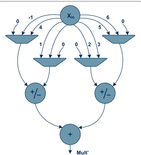
The PEs are the basic units of the proposed unified trans-form architecture and are responsible for realizing all the operations involved in the computation of the consid-ered 1-D transforms. Within the systolic array, all the PEs share the same architecture and perform the same set of operations, which mostly consist of the multiply-and-accumulate (MAC) operations involved in the transform computation procedure. As it can be seen in Figure 2, which depicts the generic block diagram of a PE, the architecture of these processing structures is composed of two main blocks: acontrol moduleand anarithmetic module.
The control module is responsible for guaranteeing the correct flow of all the control signals of the architecture inside the systolic array, giving support to the dataflow model described in Section 4.1. Furthermore, it is also responsible for generating the control signals that com-mand the transform computation procedure inside the PE. One of the key operations that is realized by this module consists in the generation of the multiplier val-ues (i.e. the transform kernel valval-ues) to be used in the MAC operations that are performed in the PE. Such values are generated by taking into consideration the horizon-tal and vertical coordinates of the PE inside the systolic array, as well as the type of transform that must be computed.
The rationale behind the algorithm that was imple-mented to generate the kernel values for any given DCT results from the observation that only N − 1 differ-ent basis values exist in a N ×N transform kernel [6]. These values consist of the first column of the trans-form kernel (e.g. see (1) and (2)), which correspond to the subset of kernel values matching the DCT cosine angles in the range 0,π2 . Consequently, they can also
be used to generate the remaining (N−1) × (N−1)
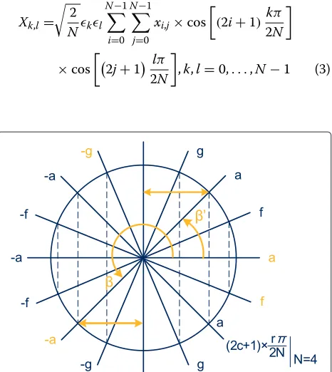
values of the transform kernel, provided that the sym-metry and periodicity trigonometric properties of the cosine function are properly exploited. This is illustrated in Figure 3 for the case of the generic 4×4 transform ker-nel presented in (1), where the value located at position (2,2) of the transform kernel (−a) is obtained by reduc-ing the correspondreduc-ing angle (β) to an elementary angle (β) located in the first quadrant of the trigonometric circle.
To implement the devised algorithm, the control mod-ule of the PEs makes use of a quite simple
combina-tional circuit (identified asMultiplier Decoder in
Figure 2) and of a small ROM. Together, they generate all the multiplier values corresponding to all the kernel val-ues of the considered transforms. The operation of such circuit for aN×Ntransform kernel is the following.
Figure 2Generic block diagram of the PE.
transforms), as specified in the generic formulation of the 2-D DCT shown in (3).
Xk,l =
2 Nkl
N−1
i=0
N−1
j=0
xi,j×cos
(2i+1)kπ 2N
×cos2j+1 lπ 2N
,k,l=0,. . .,N−1 (3)
Figure 3Definition of a transform kernel value.Definition of the value (−a) located at position (2,2) of the generic 4×4 transform kernel shown in (1), according to the proposed algorithm.
t=
1
√
2 , ift=0
1 , otherwise (4)
Although such computations should be performed with integer arithmetic by using 2×log2N+1 bits, only the
log2N+2 least significant bits off are of practical inter-est, because they identify the corresponding angular value constrained to the range [0, 2π[. The remaining bits only specify the amount of times the 2πdomain was exceeded and therefore can be ignored. To exemplify this procedure, Figure 3 illustrates the definition of all the angles corre-sponding to the entries of the generic order-4 transform kernel (N = 4) presented in (1). In particular, the angles corresponding to all the values in the second column of this matrix (c = 2;r = 0. . .3) are also highlighted in yellow colour ((r,c)→β=f ×2π×4).
The two most significant bits of the obtained con-strained result (f = f<log2N+1:0>) are then evaluated, in
order to determine if the corresponding angle is in one of the following rangesπ2,π ,π,32π or32π, 2π . In such cases, the constrained valuefis computed, which corre-sponds to a reduction of the original angle into the range
Finally, the sign information of the kernel value is com-puted by considering the two most significant bits off. If such data corresponds to an angle in the rangeπ2,32π (1 ≤ f<log
2N+1:log2N> ≤ 2), the considered transform kernel entry represents a negative number. Otherwise, it represents a positive number.
As it can be seen in Figure 2, the obtained multiplier control word and the corresponding sign information bit are not directly applied to the multiplication circuit embedded in the PE. Instead, such data is stored in an internal data-standing register of the PE, so that it can be used to compute the MAC operations in the subsequent clock cycles. This approach allows to significantly improve the processing rate of the PEs, since it greatly reduces the critical path of the circuit. This aspect is of utmost importance in the proposed unified transform architec-ture, because all the computations that are performed in the arithmetic module of the PEs are realized using integer arithmetic circuits with a relatively high resolu-tion, as a result of the increased dynamic gains imposed by the higher order transform kernels considered in the state-of-the-art video standards (e.g. HEVC [4]).
Nevertheless, this procedure also imposes an explicit PE configuration stage prior to the computation of a new transform, whenever the architecture is reprogrammed to make use of a different transform kernel. In such cases, the PEs are also configured in a wavefront manner, just like in the dataflow model described in Section 4.1. The com-mand that triggers such event is also sent through the top left corner PE, which then propagates it to the remaining PEs in both the horizontal and vertical directions. Since this operation requires only one single clock cycle and is performed in a pipelined fashion, it is possible to start the computation of a new transform operation in each PE on the clock cycle that immediately succeeds its recon-figuration stage. As a result, only when it is necessary to compute a new transform involving a kernel different from the one currently in use within the systolic array does the PE reprogrammable architectural feature increase the latency of the unified transform architecture in one single clock cycle.
The arithmetic module of the PEs makes use of an accumulator and of a specialized multiplication circuit to perform all the required transform operations. In this scope, the data values to be processed (Xin) are placed at one of the inputs of the multiplier. Conversely, the partial value of the transform operation being computed (ACC_in), which was calculated by an adjacent PE in the previous clock cycle, is placed at one of the inputs of the accumulator. Then, this partial value is updated with the result of the multiplication involvingXin and the kernel value corresponding to the multiplier control word stored in the internal standing-data register of the PE, by also taking into consideration the sign information bit stored
in the same internal standing-data register. The resulting value is stored in another internal standing-data register before being propagated to the following PEs in the array, in order to shorten the critical path of the architecture and to guarantee the systolic dataflow.
This highly flexible PE architecture allows the designer to easily adapt the PE functionality, so that multiple and distinct transform kernels can be supported. In fact, in order to design a new PE structure that is capable of sup-porting one or more transform kernels, it is only necessary to encode the considered kernel values in the ROM and develop a new multiplication circuit. By jointly exploiting this feature and the modularity and reconfigurable prop-erties of the presented unified architecture, it is possible to realize several different transform cores addressing not only the subset of transforms that are used by a specific video standard but also more generic MST cores. In this work, all these properties were extensively exploited, in order to design a new set of PEs addressing the AVC, AVS, VC-1 and HEVC standards. In addition, a multi-standard PE that is capable of processing the transforms defined in all these standards by using a resource-shared mul-tiplication circuit was also developed. To better explain the procedures involved in the design of all these PEs, the following subsection presents a brief review of all the development stages of the proposed multi-standard PE, which is taken as a case study.
4.3 Resource-shared multi-standard PE
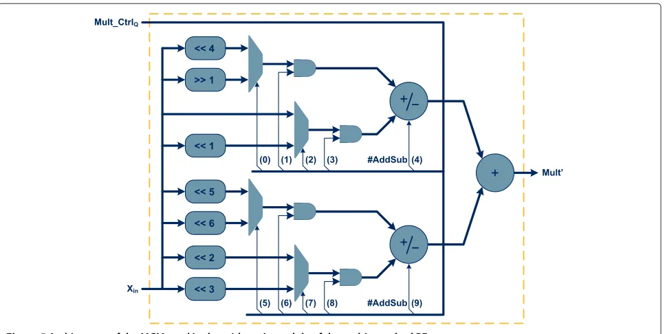
In order to fully support the computation of all the transforms defined in the AVC, AVS, VC-1 and HEVC standards, a multi-standard PE for the proposed unified transform architecture must be capable of computing all the MAC operations required by 28 different transforms (see Section 2). This involves 80 distinct transform kernel values in the range of−90 to+90. However, only one of these constants is used by the PE to perform the required MAC operation at any moment. Consequently, this opens the opportunity to make use of time-multiplexed multiple constant multiplication (MCM) structures [35], in order to implement reduced-area and faster multipliers for the PE.
extra savings, since they allow the sharing of common subexpressions for the computation of the p constants. The considered DAG fusion algorithm is applied in a later development stage, in order to ‘fuse’ the addition chains of the several individual constants into a single net-work of adders, wired shifts and multiplexers, suitable for time-multiplexing. Furthermore, the application of this algorithm also guarantees that the resulting fused addition chain circuit only includes as many adders as the largest of its fundamental addition chains.
In what concerns the proposed multi-standard PE, which implements the architecture presented in Figure 2, the first step in the design of its time-multiplexed MCM consisted in the definition of a DAG, representing an optimal addition chain, for each one of the considered kernel values (i.e. the basis values of all the considered transform kernels presented in Table 1). The next design step aimed at finding and exploiting the similarities in all these graphs, in order to obtain the best composite DAG jointly representing the addition chains of all the individ-ual DAGs. Such graph consists exclusively of additions, shifts and multiplexers, as it can be seen in Figure 4. Then, a proper hardware structure was devised to implement the DAG that was obtained in the previous design step. As it can be seen in Figure 5, such circuit requires only three adders and four (2 : 1) multiplexers, in order to perform all the MAC operations involved in the computation of the 28 transforms considered in the AVC, AVS, VC-1 and HEVC
Figure 4DAG of the MCM used in the arithmetic module of the multi-standard PE.
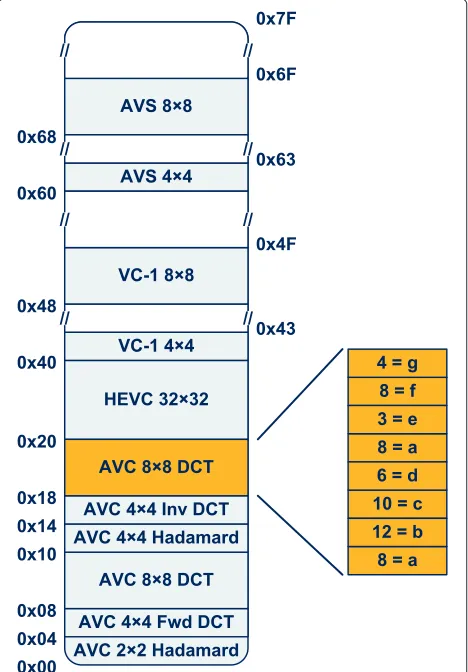
standards. In the following design step, a 10-bit control word was defined for each one of the considered ker-nel values. These 10-bit words are used to command the operation of all the multiplexers and addition/subtraction circuits composing the hardware structure obtained in the previous design step. Such control words are presented (in hexadecimal notation) in Table 2 for the set of kernel val-ues shown in Table 1. Finally, the contents of the ROM that is embedded in the control module of the proposed multi-standard PE were specified, by properly disposing all the multiplier control words in 11 different memory segments.
As it can be seen in Figure 6, each one of these memory segments concerns a distinct transform kernel of order-N, which can be addressed by using theType_Tsignal, according to the data presented in Table 3. Within each
memory segment,N consecutive memory positions are
occupied with the multiplier control words corresponding to theNbasis values of the considered transform kernel. This data is disposed in the same manner as its corre-sponding kernel values in the first column of the trans-form kernel matrix. As a result, in order to address and retrieve a given transform kernel value from the PE ROM, it is only necessary to combine the bits of theType_T
signal with those of the address value generated by the
Multiplier Decoderblock (f), which represents the offset inside the memory segment.
Consequently, by using this memory layout to program the multi-standard PE ROM with all the multiplier control words required by the the AVC, AVS, VC-1 and HEVC standards, it was possible to greatly reduce the complexity
of theMultiplier Decoderin the PE.
5 Experimental evaluation
The advantages offered by the proposed unified trans-form architecture in the design of high-pertrans-formance and dedicated MST cores were experimentally assessed using FPGA realizations. The implemented processing struc-tures are based on a systolic array with 8×8 PEs, which was configured to support the computation of the trans-forms defined in the AVC, AVS and VC-1 standards, as well as the 4×4 and 8×8 HEVC transforms, by using the PEs presented in Section 4.2.
Figure 5Architecture of the MCM used in the arithmetic module of the multi-standard PE.
order-8, because most of the existing alternative designs are based on this configuration setup.
It should be noted that the chosen architecture config-uration does not compromise either the relevance of the proposed unified architecture or the benefits that it offers in terms of performance and functionality when com-pared with other alternative solutions, as is discussed in Section 5.2.
5.1 FPGA implementation
The considered hardware realizations were synthesized and implemented in a Xilinx Virtex-7 XC7VX485T FPGA device, by using the Xilinx ISE 13.1i tool chain and a parameterizable IEEE-VHDL description of the presented unified transform architecture and of all the proposed PEs. Such generic architectural descriptions follow a strict modular approach using independent and self-contained functional blocks, in order to comply with the scalabil-ity and multi-transform requirements of the architecture. Table 4 presents the implementation results of the devised PEs, while Table 5 summarizes the hardware realization of the considered MST core. All the presented results were
obtained by performing a standard synthesis procedure, targeting performance optimized circuits.
The results presented in Table 4 demonstrate the reduced hardware cost of the devised PEs, since all the considered implementations require between 10 and 14 Virtex-7 slices. As it was expected, the multi-standard PE is the processing structure that requires more hardware resources, due to the increased flexibility that is offered to support the computation of all the transforms defined in the AVC, AVS, VC-1 and HEVC standards. Accordingly, it is also the processing structure presenting the lowest value for the maximum clock frequency, i.e. 285.3 MHz. Again, this is a result of its ability to perform the trans-form computations involving 80 different kernel values, which requires not only a MCM with a longer latency, due to the usage of two adders interconnected in cascade (see Figure 5), but also arithmetic circuits with a larger bit width in the datapath of the PE (i.e. 38 bits for input values originally encoded with 16 bits), as a result of the increased dynamic gain of the HEVC transform kernels (i.e. 22 bits). Since the dynamic gains of the AVC, VC-1 and AVS transform kernels are relatively lower (i.e. 12, 13
Table 2 Multiplier control words for the AVC, AVS, VC-1 and HEVC transform kernels (see Table 1)
Kernel value 12 1 2 3 4 6 8 9 10 12
ROM word 0×3 0×8 0×C 0×118 0×100 0×10C 0×180 0×188 0×18C 0×2FD
Kernel value 15 16 18 36 50 64 75 83 89
Figure 6Memory map of the ROM used in the multi-standard PE.
and 14 bits, respectively), the bit width of the arithmetic circuits composing the datapaths of the PEs that were designed to exclusively address such standards is therefore smaller.
As it can be seen in Table 4, such characteristic allows these PEs to be operated using relatively higher clock frequencies. The highest clock frequency corresponds to the AVS PE, due to the simplicity and the lower latency of the involved MCM that includes only a sin-gle adder/subtractor. Nevertheless, all the clock frequency values that are presented in Table 4 clearly evidence the high processing rates that are offered by all the devised PEs. In fact, from these results, it can concluded that any of these PEs can be used in the processing of video sequences with resolutions as high as 7,680×4,320 pix-els (i.e. the 8k Ultra inition Television (UHDTV) format) in real time.
This conclusion can be easily extrapolated from Table 5, which shows that the implemented MST core is able not only to compute up to 17.9 giga operations per second (GOPS) but also to offer a sustained processing through-put of about 2.2 ×10⁹ samples per second (GSamp/s),
Table 3 Encoding of theType_Tsignal for the implementation of the MST core
Type_T Transform kernel
0 AVC 2×2 Hadamard
1 AVC 4×4 Hadamard
2 AVC 4×4 forward DCT
3 AVC 8×8 forward DCT
4 AVC 2×2 Hadamard
5 AVC 4×4 Hadamard
6 AVC 4×4 inverse DCT
7 AVC 8×8 inverse DCT
8 HEVC 4×4 DCT
9 HEVC 8×8 DCT
10 VC-1 4×4 DCT
11 VC-1 4×8 DCT
12 VC-1 8×4 DCT
13 VC-1 8×8 DCT
14 AVS 4×4 DCT
15 AVS 8×8 DCT
by using a clock frequency of 279.6 MHz. These rela-tively high performance levels are very similar to the ones provided by the design that was proposed in [7], despite such processing structure is only capable of computing the transforms defined in the AVC and HEVC standards. This result was already expected and is due to the follow-ing two reasons: (i) the pipelined processfollow-ing nature of the presented unified transform architecture and (ii) the quite similar latency values imposed by the devised PEs, which is a result of their highly optimized and almost identical internal hardware structure.
The results that are presented in Table 5 also demon-strate the quite reduced hardware cost of the devised proof-of-concept MST architecture, while offering a remarkable processing rate. As it can be seen, less than 4% of the total hardware resources available in the adopted medium-size FPGA device were used in the realization of
Table 4 Implementation results of the devised PEs in a Xilinx Virtex-7 FPGA
Processing structure Registers LUTs Maximum frequency [MHz]
PE for AVC 67 124 371.5
PE for AVS 66 111 395.3
PE for VC-1 65 160 302.0
PE for HEVC 79 253 289.3
Table 5 Implementation results of the proof-of-concept MST core in a Xilinx Virtex-7 FPGA
Processing structure Registers LUTs Maximum frequency [MHz]
MST core 7,309 21,568 279.4
Input buffer 1,681 1,265 388.7
Array with 8×8 PEs 5,332 18,624 284.1
PE 80 299 285.3
Transposition switch 1,362 2,161 417.4
Control unit 97 77 573.1
the considered transform core. Almost all of these hard-ware resources (about 86%) are used to implement the 2-D systolic array, with each of its 8×8 multi-standard PEs requiring at most 14 slices. Therefore, it can be observed that while the hardware cost of the presented unified architecture mostly results from the adopted configura-tion for its systolic array, its maximum clock frequency is only limited by the critical path of the PEs. Consequently, it can be expected that very similar performance levels will be attained for other configurations of the proposed uni-fied architecture making use of larger systolic arrays (e.g. an array with 32×32 PEs, to allow the computation of the higher order transforms defined in HEVC).
5.2 Comparative analysis
In order to further demonstrate the advantages that are offered by the presented unified architecture in the design of video codecs supporting the most recent and state-of-the-art video standards, several different alternative designs recently described in the literature for this domain
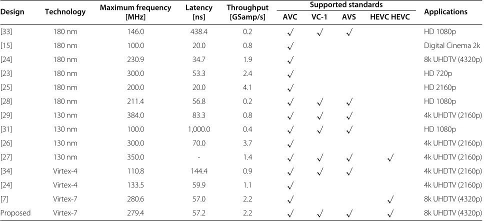
were reviewed. Due to the diverse set of technologies that are considered in the implementation of these designs, as well as to the different functionalities that are presented by each implementation and the distinct considerations that might have been adopted, this analysis mostly focused on a comparison of the functionalities and computational rates offered by the various structures. Table 6 summa-rizes the results of such comparative analysis for a subset of the most related and prominent designs that were eval-uated. Note that the presented data concerns only to the implementation of the transform computation module(s) of the considered transform cores.
A straightforward analysis of the data presented in Table 6 clearly shows that only a few of the reviewed designs are able to offer a multi-standard functionality. In addition, it also evidences that only the designs pre-sented in [7,27] are able to support the computation of the HEVC transforms. Nevertheless, it should be noted that while the architecture presented in [7] is capable of realizing the complete set of transforms defined in the standard, the one proposed in [27] is able to compute only the HEVC inverse transforms. Therefore, the application domain of this processing structure is limited to the design of high-performance decoders, being unsuitable to imple-ment video encoders. This characteristic is common to many of the designs enumerated in Table 6, since they are able to compute only a subset of the transforms defined in one or multiple video standards [23,24,26,28,29,33]. In fact, to the best of the authors’ knowledge, the MST architecture herein proposed is one of the first structures that is able to compute the complete set of transforms adopted in the AVC, AVS, VC-1 and HEVC standards.
Table 6 Functional and performance comparison with other architectures
Design Technology Maximum frequency Latency Throughput Supported standards Applications
[MHz] [ns] [GSamp/s] AVC VC-1 AVS HEVC HEVC
[33] 180 nm 146.0 438.4 0.2 √ √ √ HD 1080p
[15] 180 nm 100.0 20.0 0.8 √ Digital Cinema 2k
[24] 180 nm 230.9 34.7 1.9 √ 8k UHDTV (4320p)
[23] 180 nm 300.0 53.3 2.4 √ HD 720p
[25] 180 nm 200.0 20.0 4.1 √ HD 2160p
[28] 180 nm 211.4 56.8 0.2 √ √ √ HD 1080p
[29] 130 nm 384.0 83.3 0.8 √ √ √ 4k UHDTV (2160p)
[31] 130 nm 100.0 1,000.0 0.4 √ √ √ HD 1080p
[26] 130 nm 300.0 70.0 3.7 √ 4k UHDTV (2160p)
[27] 130 nm 350.0 - 1.4 √ √ √ √ 4k UHDTV (2160p)
[34] Virtex-4 110.8 144.4 0.9 √ √ √ 4k UHDTV (2160p)
[24] Virtex-4 133.5 59.9 1.1 √ 4k UHDTV (2160p)
[7] Virtex-7 280.6 57.0 2.2 √ √ 8k UHDTV (4320p)
In what concerns the offered performance levels, the comparison that is presented in Table 6 clearly shows that the implemented transform core offers one of the high-est computation rates (2.2 GSamp/s), despite being one of the few designs with enhanced multi-standard trans-form computation capabilities. In fact, it can be observed that this design outperforms almost all the other consid-ered architectures by about 1.8 times. The only exceptions are the designs presented in [7,23,26]. However, these faster processing structures are able to compute only a quite reduced subset of the transforms supported by the devised proof-of-concept transform core, since they were either specifically designed to accelerate the inverse 8×8 DCT [23], optimized for the implementation of the for-ward transform coding path of a video encoder [26], or only support the AVC and HEVC standards [7].
The results presented in Table 6 also demonstrate that the proposed unified transform architecture allows to design MST cores that impose very small latency in the processing of the video bit streams, when compared to the majority of the considered alternative designs. This is a quite important aspect when real-time operation is con-sidered, since the latency that is imposed to the processing of each video frame may compromise the operation of the codec in ‘live’ mode.
6 Conclusions
A high-performance unified architecture for the compu-tation of a vast set of 2-D transforms adopted by several modern video standards is proposed in this paper. To the best of the authors’ knowledge, this is one of the first structures that is capable of computing all the DCTs of dif-ferent orders (e.g. order-4, order-8, order-16 and order-32) that are adopted in the AVC, AVS, VC-1 and HEVC stan-dards. Contrasting to other dedicated transform cores, the presented architecture is supported on a completely con-figurable and scalable structure, capable of providing the processing rates that are required to compute, in real time, all the transforms in HD video sequences. When proto-typed in a Xilinx Virtex-7 FPGA device, an MST core based on the proposed unified architecture is able to com-pute up to 17.9 GOPS and offer a sustained throughput of about 2.2×10⁹samples per second, by using a clock fre-quency of 279.6 MHz. Such relatively high performance levels allow this hardware structure, supporting the AVC, AVS, VC-1 and HEVC standards, to process in real-time 8k UHDTV (7,680×4,320) sequences at a frame rate of 30 fps.
Competing interests
The authors declare that they have no competing interests.
Acknowledgements
This work was supported by national funds through Fundação para a Ciência e a Tecnologia (FCT) under the project PEst-OE/EEI/LA0021/2013 and by the Programa de apoio à Formação avançada de docentes do Ensino Superior
Politécnico (PROTEC) programme funds, under the research grant SFRH/PROTEC/50152/2009.
Author details
1INESC-ID, Rua Alves Redol, 9, Lisbon 1000-029, Portugal.2IST, Universidade de Lisboa, Avenida Rovisco Pais, 1, Lisbon 1049-001, Portugal.3ISEL, Instituto Politécnico de Lisboa, Rua Conselheiro Emídio Navarro, 1, Lisbon 1959-007, Portugal.
Received: 1 March 2014 Accepted: 30 June 2014 Published: 11 July 2014
References
1. T Wiegand, G Sullivan, G Bjntegaard, A Luthra, Overview of the H.264/AVC video coding standard. IEEE Trans. Circ. Syst. Video Tech.13(7), 560–576 (2003)
2. L Yu, S Chen, J Wang, Overview of AVS-video coding standards. Signal Process. Image Comm.24(4), 247–262 (2009)
3. S Srinivasan, SL Regunathan. Vis. Commun. Image Process.5960, 720–728 (2005)
4. K Ugur, K Andersson, A Fuldseth, G Bjontegaard, LP Endresen, J Lainema, A Hallapuro, J Ridge, D Rusanovskyy, C Zhang, A Norkin, C Priddle, T Rusert, J Samuelsson, R Sjoberg, Z Wu, High performance, low complexity video coding and the emerging HEVC standard. IEEE Trans. Circ. Syst. Video Tech.20(12), 1688–1697 (2010)
5. Z-N Li, MS Drew,Fundamentals of Multimedia, 1st. (Prentice Hall, New Jersey, 2003)
6. KR Rao, P Yip,Discrete Cosine Transform: Algorithms, Advantages, Applications. (Academic Press, San Diego, 1990)
7. T Dias, N Roma, L Sousa, High performance multi-standard architecture for DCT computation in H.264/AVC high profile and HEVC codecs, in Conference on Design & Architectures for Signal and Image Processing (Cagliari, 2013), pp. 14–21
8. W-K Cham, Development of integer cosine transforms by the principle of dyadic symmetry. Commun. Speech Vision IEEE Proc. I.136(4), 276–282 (1989)
9. C Zhang, L Yu, J Lou, W-K Cham, J Dong, The technique of prescaled integer transform: concept, design and applications. IEEE Trans. Circ. Syst. Video Tech.18(1), 84–97 (2008)
10. J-J Lee, S Park, N Eum, Design of application specific processor for H.264 inverse transform and quantization, inInternational SoC Design Conference, vol. 2 (Busan, 2008), pp. 57–60
11. NT Ngo, TTT Do, TM Le, YS Kadam, A Bermak, ASIP-controlled inverse integer transform for H.264/AVC compression, inThe 19th IEEE/IFIP International Symposium on Rapid System Prototyping(Monterey, 2008), pp. 158–164
12. J Shan, C Chen, E Yang, High performance 2-D IDCT for image/video decoding based on FPGA, inInternational Conference on Audio, Language and Image Processing(Shanghai, 2012), pp. 33–38
13. W-H Chen, C Smith, S Fralick, A fast computational algorithm for the discrete cosine transform. IEEE Trans. Comm.25(9), 1004–1009 (1977) 14. C-P Fan, Fast 2-dimensional 4x4 forward integer transform
implementation for H.264/AVC. IEEE Trans. Circuits Syst. II.53(3), 174–177 (2006)
15. K-H Chen, J-I Guo, J-S Wang, A high-performance direct 2-D transform coding IP design for MPEG-4AVC/H.264. IEEE Trans. Circ. Syst. Video Tech. 16(4), 472–483 (2006)
16. S Shen, W Shen, Y Fan, X Zeng, A unified forward/inverse transform architecture for multi-standard video codec design. IEICE Trans. Fund. Electron. Comm Comput. Sci.96-A(7), 1534–1542 (2013)
17. JS Park, WJ Nam, SM Han, S Lee, 2-D large inverse transform (16x16, 32x32) for HEVC (high efficiency video coding). J. Semicond Technol. Sci. 12(2), 203–211 (2012)
18. L Ling-Zhi, Q Lin, P Meng-tian, J Li, A 2-D forward/inverse integer transform processor of H.264 based on highly-parallel architecture, in4th IEEE International Workshop on System-on-Chip for Real-Time Applications (Banff, 2004), pp. 158–161
20. RB Are, K Rajan, An RNS based transform architecture for H.264/AVC, in 2008 IEEE Region 10 Conference TENCON(Hyderabad, 2008), pp. 1–6 21. C-C Sun, P Donner, J Götze, VLSI implementation of a configurable IP core
for quantized discrete cosine and integer transforms. Int. J. Circ. Theor. Appl.40(11), 1107–1126 (2012)
22. Y-H Chen, J-N Chen, T-Y Chang, C-W Lu, High-throughput multistandard transform core supporting MPEG/H.264/VC-1 using common sharing distributed arithmetic. IEEE Trans. Very Large Scale Integrat. Syst. PP(99), 1–1 (2013)
23. C Jiang, N Yu, M Gu, A novel VLSI architecture of 8x8 integer DCT based on H.264/AVC FRext, in3rd International Symposium on Knowledge Acquisition and Modeling(Wuhan, 2010), pp. 59–62
24. TTT Do, TM Le, High throughput area-efficient SoC-based forward/inverse integer transforms for H.264/AVC, inIEEE International Symposium on Circuits and Systems(Paris, 2010), pp. 4113–4116
25. W Hwangbo, C-M Kyung, A multitransform architecture for H.264/AVC High-Profile coders. IEEE Trans. Multimed.12(3), 157–167 (2010) 26. M Gu, N Yu, C Jiang, W Lu, Hardware prototyping for various transforms in
H.264 high profile. J. Inform. Comput. Sci.8(1), 119–128 (2011) 27. S Shen, W Shen, Y Fan, X Zeng, A unified 4/8/16/32-point integer IDCT
architecture for multiple video coding standards, inIEEE International Conference on Multimedia and Expo(Melbourne, 2012), pp. 788–793 28. M Martuza, C McCrosky, K Wahid, A fast hybrid DCT architecture
supporting H.264, VC-1, MPEG-2, AVS and JPEG codecs, in11th International Conference on Information Science, Signal Processing and Their Applications(Montreal, 2012), pp. 545–549
29. T Ho, T Le, K Vu, S Mochizuki, K Iwata, K Matsumoto, H Ueda, A 768 megapixels/sec inverse transform with hybrid architecture for multi-standard decoder, inIEEE International Conference on ASIC(Xiamen, 2011), pp. 71–74
30. Y-K Lai, Y-F Lai, A reconfigurable IDCT architecture for universal video decoders. IEEE Trans. Consum. Electron.56(3), 1872–1879 (2010) 31. K Wang, J Chen, W Cao, Y Wang, L Wang, J Tong, A reconfigurable
multi-transform VLSI architecture supporting video codec design. IEEE Trans. Circ. Syst. II.58(7), 432–436 (2011)
32. Y Li, Y He, S Mei, A highly parallel joint VLSI architecture for transforms in H.264/AVC. J. Signal Process. Syst.50(1), 19–32 (2008)
33. K Wahid, M Martuza, M Das, C Mc Crosky, Resource shared architecture of multiple transforms for multiple video codecs, in24th Canadian Conference on Electrical and Computer Engineering(Niagara Falls, 2011), pp. 947–950
34. G Liu, An area-efficient IDCT architecture for multiple video standards, in 2nd International Conference on Information Science and Engineering (Hangzhou, 2010), pp. 3518–3522
35. P Tummeltshammer, JC Hoe, M Puschel, Time-multiplexed multiple-constant multiplication. IEEE Trans. Comput. Aided Des. Integrated Circ. Syst.26(9), 1551–1563 (2007)
36. F Bergeron, J Berstel, S Brlek, Efficient computation of addition chains. J. de théorie des nombres de Bordeaux.6(1), 21–38 (1994)
doi:10.1186/1687-6180-2014-108
Cite this article as:Diaset al.:Unified transform architecture for AVC, AVS,
VC-1 and HEVC high-performance codecs.EURASIP Journal on Advances in
Signal Processing20142014:108.
Submit your manuscript to a
journal and benefi t from:
7Convenient online submission 7 Rigorous peer review
7Immediate publication on acceptance 7 Open access: articles freely available online 7High visibility within the fi eld
7 Retaining the copyright to your article
![Figure 1 Block diagram of the architecture presented in [7].](https://thumb-us.123doks.com/thumbv2/123dok_us/895821.1107900/7.595.58.542.84.343/figure-block-diagram-architecture-presented.webp)