881 | P a g e
STUDY AND IMPLEMENTATION OF PHASE
LOCKED LOOP
Dr. Sunita Pandit Ugale
1, Rasika Madhukar Chandramore
21,2
Department of Electronics & Telecommunications, K.K.W.I.E.E.R, Nashik, (India)
ABSTRACT
This paper introduces a design aspects of low power phase locked loop using VLSI technology.The phase locked
loop is designed using latest 45nm process technology parameters, which in turn offers high speed performance
at low power. The main quality related to the 45nm technology such as the high-k gate oxide ,metal-gate and
very low-k interconnect dielectric described.
Keywords— Phase locked loop (PLL), voltage control oscillator (VCO), 45nm technology, Very large scale
integration (VLSI) technology, low power.
I.INTRODUCTION
A phase locked loop system is negative f/b system where an signal which generate oscillator is phase and
frequency locked to a reference signal. A reference signal is usually retrieved from a crystal oscillator. A crystal
oscillator reference is kept in MHz range and is consider to be the most stable form of oscillator available. High
frequency crystals are really expensive and hence not used in the system to reduce overall costs.
More precisely ,a PLL circuit synchronizes an output signal (phase and frequency) with respect to references.
When the PLL gets locked the phase error between output and input signal is zero or should remain at a constant
phase error. If the frequency of reference and output gets locked but not the phase, then the PLL system disrupts
the output again and keeps running unless both phase and frequency gets locked. Therefore a control mechanism
develops unless the phase is fully locked, and thus the name phase locked loop. Basically there are three
fundamental blocks in PLL, namely :
1. Phase detector
2. Loop filter
3. VCO
II.IMPLEMENTATIONOF PLLCIRCUITS
A. Phase Frequency Detector
Phase Detector are merged, such that it can detect both phase and As the name suggest that the phase detector and
the frequency frequency differences. It is only possible for the periodic signals [11]. It consists of two
edge-triggered resettable D-flip-flops with their D inputs connected to logic 1. The reference frequency signal (A) and
the signal derived from its divider output (B) form the two inputs of the flip-flops and QA (UP) and QB (DOWN)
are the outputs [7]. This circuit shown in figure 2 compares the phase and frequency of these two input signals and
882 | P a g e
Fig 1:Block Diagram of PFD
B. Low Pass Filter
It is imperative to note that the output translated from the phase detector output consists of a undesirable high-frequency components and a desirable dc component. Thus, the low pass filter is one of the key design components which serve to effectively filter out the undesired AC component and provides a steady control voltage or the dc
level to operate the VCO [8].
C. Voltage Controlled Oscillator
A voltage controlled oscillator or VCO is the main block Of PLL system. All the blocks apart from VCO make its
frequency and phase stable. More precisely they are designed to control the VCO phase and frequency with
respect to reference. The maximum operating frequency of the VCO also decides the maximum output frequency
of the PLL system.
III. NOISE IN PLL
The total noise of the PLL is nothing but the summation of the individual noise contribution of different PLL
building blocks. The VCO and frequency divider are the blocks which contribute most of the noise in a
PLL ,because they are the blocks which are dealing with the high frequency signal .The other blocks such as
PFD ,loop filter can be designed in such a way that they will not contribute noise significantly to the PLL.
Phase noise is the measure of variations in the frequency domain. Figure 6 shows a plot of a VCO signal
exhibiting phase noise .If the phase noise was not present ,the entire power of the oscillator would be focused at
the center frequency W0.However , the phase noise spreads some of the oscillator power to adjacent
frequencies ,which results in the sidebands.
883 | P a g e
IV. SIMULATION RESULTS
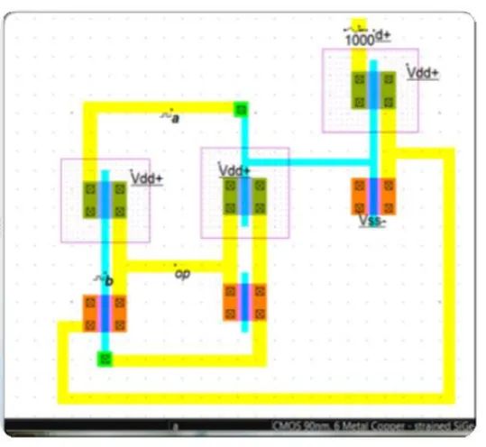
Fig 3 :Layout of XOR Phase Detector
The clock skew is minimized by using single edge clocks.The operating range of the design is increased with the
help of synchronous CMOS logic and also the power consumption is reduced compared to the traditional PFD.
The output of the PFD when reference signal rising edge leads input signal rising edge and vice versa is shown in
fig 4.The XOR phase detector simply verify truth table of the XOR gate or we can say it detect when there is any
change in
its input phase.
Fig 4 : o/p waveform of XOR PFD
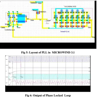
The transient response of the PLL is as shown in figure 5. Here it can be observed that the filter output comes to stable after a period of 220 ns which is called as settling time or lock in time.
884 | P a g e
reference and the feedback input signal also remains constant. But there is an offset phase difference throughout the time period .
Fig 5: Layout of PLL in MICROWIND 3.1
Fig 6: Output of Phase Locked Loop
V. COMPARISON CHART OF VARIOUS TECHNOLOGIES
Technology 90nm 45nm 30nm
Area 55.5um2 35.6um2 22.8um2
Power 0.268mW 2.074uW 1.679uW
Delay 102.3Ps 153Ps 102.3Ps
Frequency 2.55GHz 2.55GHz 2.55GHz
Width 17.7um 8.8um 7.1um
Height 8.1um 4.0um 3.2um
VI. CONCLUSION
A phase locked loop with low phase noise is designed here.The lock time and lock range are also measured. The
-885 | P a g e
91.74dBc/Hz at 1MHz offset frequency. We also compare the study at various technology. The center frequencyof oscillation of VCO.
[1] T.R Lee and A Hajimiri, "Oscillator Phase Noise: a Tutorial," IEEE Journalo/Solid-State Circuits. vol. 35,
March 2012, pp. 326 - 336.
[2] M.Mansuri, D.Liu, and C.K.Yang, "Fast Frequency Acquisition Phase Frequency Detector forGSamples/s
Phase Locked Loops," IEEE Journal o/Solid State Circuit, Vol. 37, No. 10, Oct., 2013.
[3] S. M. Shahruz, "Novel phase-locked loops with enhanced locking capabilities,"Journal 0/ Sound and Vibration,
Vol. 241, Issue 3, 29 March 2013.
[4] William Shing Tak Yan, Howard Cam Luong, A 900-MHz CMOS Low Phase Noise Voltage Controlled Ring
Oscillator, IEEE Transactions on Circuits and Systems-II: Analog and Digital Signal Processing, Vol. 48, No.
2, February 2011.
[5] Ullas Singh, Michael Green, Dynamics of High-Frequency CMOS Divide IEEE, 0-7803-7448-7/02, V -
421-424, 2012.
[6] Zhongtao Fu, Xiao Wang, Eugene Minh, Alyssa Apsel, A Fast Acquisition Phase Frequency Detector for
Phase Locked Loop, Proceedings of the Argentine school of Micro Nanoelectronics, Technology and
Application, pg 77-80,2013.
[7] Behzad Razavi, Design of Analog CMOS Integrated Circuits, McGraw-Hill Higher Education, 2013.
[8] Best, Roland E. Phase-Locked Loops Design, Simulation and Application MacGraw- Hill, 2010.
[9] Phase Locked Loops Design, Simulation and Applications,"McGraw-Hill Publication, 5th Edition, 2014.
[10] Bianchi, Giovanni. Phase-Locked Loop Synthesizer Simulation. McGrawHill, 2012.
[11] Chou, Chien-Ping, Lin, Zhi-Ming,and Chen, Jun-Da. A 3-PS Dead-Zone Double- Edge-checking
Phase-Frequency-Detector With 4.78 GHz Operation Frequency:The 2004 IEEE Asia-Paci_c Conference on Circuits
and Systems conference. (2012) : Volume 2, Page(s): 937 940.
[12] Barrett, Curtis. Fractional/Integer-N PLL Basics. Texas Instruments, Wireless Communication Business Unit,