State Space Model for 3-Phase 4-Wire
DSTATCOM under Unbalanced Distorted
Supply Voltages
K SrinivasAssistant Professor, Dept. of EEE, JNTUH College of Engineering, Jagitial, Telangana, India
ABSTRACT: This paper presents the DSTATCOM topology for compensation of AC loads including unbalanced nonlinear loads and DC load component from its DC link in a three phase four wire system. In this the algorithm instantaneous symmetrical components used to extract positive sequence of supply voltage to generate reference compensator current to compensate AC, DC components under unbalance and non stiff supply voltage. Its state space model has derived and presented. Its state matrix components have been developed considering unbalanced non stiff source. The voltage source inverter has operated in current controlled mode and the switching pulses for filter have been developed using a two level and three level hysteresis controller. In the three level hysteresis controllers, inverter Switching strategies uses inverter zero output condition to make DC capacitor voltage constant. The simulations have done in MAT LAB.
KEYWORDS: Active power filter, AC loads, Non linear Loads, Distribution static compensator, Theory of instantaneous symmetrical components.
I.INTRODUCTION
In the last few decades, the revolt of using power electronics devises has increased very a large amount. The extensive use of power electronics based loads causes power pollution rigorously effecting in distribution systems, especially in single phase load are tapped from three phase four wire distribution systems. Because of these uneven power distributions, clean power supply to customers has challenge for power engineers. Active power filters have been developed to solve some of power quality problem which are current harmonics, low power factor and unbalanced load ect. [1-2] one of the main sections of active power filter (APF) is the voltage source inverter (VSI), operated in current controlled mode [3]. The shunt connected custom power device called the distribution static compensator (DSTATCOM), injects harmonic currents equal but opposite magnitude at a point where source, load and filter has connected called the point of common coupling (PCC) so that harmonic filtering, power factor correction, and load balancing can be achieved [4]. The operation of VSI is supported by a dc storage capacitor with proper dc voltage across the VSI (whose DC value is maintained constant) [5-6]. Control methods of the active power filter is an important criterion. There are large numbers of control methods are available to operated active power filters for.
currents are distorted [9]. This is not desirable characteristic of the algorithm. The algorithm works very well if we can find positive sequence voltages for unbalance supply voltages and substitute these voltages in control algorithm based on the instantaneous symmetrical components theory both under stiff and non stiff sources
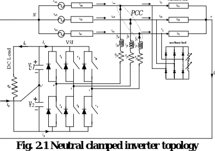
II. NEUTRAL CLAMPED INVERTER TOPOLOGY
There are various voltage source inverter are presented eminent researchers, but among those the neutral clamped inverter topology has gained considerable attention to load balancing, harmonics reduction and power factor correction. A three phase four wire neutral clamed inverter circuit has shown in Fig. 2.1. It is well published in [12-14]. In this circuit the junction (
n
) of the two capacitors is connected to the neutral of the load and source. A path for zero sequence current flows through this neutral wire. Therefore the three injected currents of voltage source inverter can be independently controlled. In this configuration there is no isolation transformer and each leg of the VSI is connected to the point of common coupling through an interface inductor with small resistance which is equivalent inductor resistance.PCC
Fig. 2.1 Neutral clamped inverter topology
The topology consists of six switches and there are no isolation transformers. The problem of saturation due to dc current does not arise due to absence of transformers. This topology employs two dc storage capacitors (C1 and C2)
of same rating. The topology provides the independent tracking of the three reference currents and compensates the zero sequence load current. However it has serious disadvantage that due dc component of load current the voltages of the capacitors do not remain constant shown in [15-16]. Because of the unequal leakage currents, unequal delay in the semiconductor switch, asymmetric charging of the capacitors during transient conditions, the state space model will be developed. This model will be used for ac load compensation, which may be unbalanced and contain harmonics. To equate the unequal capacitor voltage PI controller will be used, explained in the following section.
III. EXTRACTION OF REFERENCE COMPENSATOR CURRENTS UNDER NON STIFF AND UNBALANCED SOURCE VOLTAGES
A three phase, four wire compensated system [15] is shown in Fig.1. The three phase load considered is unbalanced and non linear, the three phase supply voltages and currents also considered unbalanced [16-17]. The compensator , linear and non linear loads are connected at a point called the point of common coupling (PCC), accordingly the compensator has to inject currents in to the line equal and opposite to load currents, then the source currents are free harmonics. The compensator is considered is idle and it is comprised of idle three phase voltage source inverter [18-19].
The basic scheme is shown in Fig. 3.1. In this scheme the compensator is represented by current sources. The
aim of the scheme is to generate the three reference current waveforms for
i
fa,i
fb andifc, denoted byi*fa,i*fb, and*
fc i
assumption on the nature of the load is required. The compensator will produce desired results as long as its bandwidth is sufficient to follow the fluctuations in the load. The reference currents are generated using the theory of the instantaneous symmetrical components.
Let any three phase instantaneous currents be defined by,ifb, i
fc and . The power invariant instantaneous symmetrical
components are then defined by.
2vdc
2vdc
h
h
1
t
T
Fig.3.1 Line diagram of 3-phase, 4-wire compensated system Fig. 4.1 Two level hysteresis current controller.
IV. PWM HYSTERESIS CURRENT CONTROLLER
The linear current controller generates required variable voltage which is then fed into single or multiple pulsed width modulation (PWM) to generate the gate drives switching pulses for voltage source inverter (VSI). The non linear current controller’s works on pre defined hysteresis band, in which the actual currents are compared with the reference compensator currents which are generated based on instantaneous symmetrical components theory under unbalanced and distorted source voltages, discussed in previous section.
4.1 Two-Level Hysteresis Current Controller
In conventional hysteresis current controller, the inverter output current is made to follow the reference current generated by the algorithm strictly with certain hysteresis band. Hysteresis current controller operates PWM voltage source inverter by comparing reference current with actual filter current in a pre defined hysteresis bands (upper and lower) shown in Fig. 4.1. The current error is difference between the desired (reference) current and the actual current generated by the inverter. The basic logic is as given below.
If the actual current in certain leg is greater than reference current plus hysteresis band (h/2) then it has to be decreased so the bottom switch has to be turned ON and top switch of the same leg has to be turned OFF at the same time. If the actual current is less than reference current minus hysteresis band (h/2) then it has to be increased so the bottom switch has to be turned OFF and top switch of same leg has to be turned ON at the same time. In this two level switching strategies does not use the inverter zero condition, it uses 2 Vdc and 2 Vdconly.
The variation of the switching frequency depends on the value of interface inductance, this variation of switching frequency influence the performance of current controlled VSI in terms of maximum switching frequency and harmonics.
4.2 Three-Level Hysteresis Current Controller [2]
instantaneous symmetrical component), at this time the inverter output is set to a zero condition and the actual current will be forced to reverse direction without reaching the next outer boundary. If the selection of a zero inverter output does not reverse the actual current, it will continue though the inner boundary to the next outer hysteresis boundary, at that time an opposite inverter output will be commanded and the current will reverse.
The switching process of three level hysteresis current controller as shown in Fig.4.2. The MATLAB program for phase-a switching is as follows.
if ierra>0 if ierra>=(h) swa=1; end
elseif ierra<=del swa=0; end
if ierra<0 if ierra<=(-h) swa=2; end
elseif ierra>=(-del) swa=0; end
If swa=1implies that the switch state is 2 Vdc elseif swa=0 implies the switch state is zero elseif swa=2 implies the switch state is 2 Vdc
Similarly for phase-b and phase-c switching functions can be performed for proper operation of three phase four wire VSI in current controlled mode. The three level hysteresis current controller frequency can be derived while considering three level switching
2vdc
2v dc
h
h
1
t
0
v dc
2
T
1
t
2
T
Fig. 4.2 Three-Level Hysteresis Current Controller
4.3 State Space Model for VSI
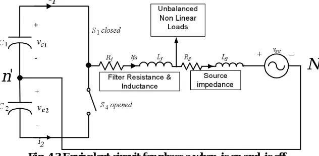
The gating signal for switch S1in Fig. 2.1 is represented by a binary variableSa. IfSa 1, S1is closed, and ifSa 0, S1is open. A gating signal for 4S is the complementary signal that is ifSa 0, 4S is open, and if Sa 1,
4
S is close. SimilarlyS
most negative group in complementary form such that in each leg one of the switches is always gated. Accordingly by operating the switches the input currents to the inverter i1 and i2 are derived from Fig. 3.3.
1
i Saifa S ib fb S ic fc (4.1)
2
i Saifa Sb fbi S ic fc (4.2)
The voltage source inverter configuration of switches S1 to S6 is operated in the three level hysteresis current
control mode. When the filter current i fa touches the pre-calculated lower limit of hysteresis band, switch S1 is closed. When the filter curent reaches to the inner band which is reference current generated usig contol theory, the swithcS1is opens and zero state will be applied. If the selection of a zero inverter output does not reverse the actual current, it will continue though the inner boundary to the next outer hysteresis boundary which 4S , will closes, at that time an opposite inverter output will be commanded and the current will reverse.
The equivalent circuit for this mode is shown in Fig 4.3.
'
n
N
1
i
2 i
Fig. 4.3 Equivalent circuit for phase a when is on and is off.
Applying KVL around the loop we get
1
v
difa Rf RS c v
sa ifa
dt Lf LS Lf LS Lf LS (4.3)
Similarly if the current hits a pre-calculated upper limit, switch is opened and is closed. From an equivalent circuit similar to Fig. 4.2, we can write,
2
c
fa f S sa
fa
f S f S f S
v
di R R v
i
dt L L L L L L (4.4)
From equation (4.3) and (4.4) combined to get the following equation.
1 2
v v
difa Rf RS c c v
sa
ifa Sa Sa
dt L LS L LS L LS L LS
f f f f
(4.5)
Similarly for phase’s b and c, we have,
1 2
c c
fb f S sb
fb b b
f S f S f S f S
v v
di R R v
i S S
dt L L L L L L L L
1 2
c c
fc f S sc
fc c c
f S f S f S f S
v v
di R R v
i S S
dt L L L L L L L L
(4.7)
In Fig. 4.3 the switch can be closed and opened or vice versa. In each case KCL can be applied at nodes 1 and 2, and KVL can be applied around the loop of the closed switch. The resulting equations can be combined with the help of (4.1) and (4.2) and binary variables and to obtain the following, assuming
1
c fa fb fc
a b c
dv i i i
S S S
dt C C C
2
fa fb fc
C
a b c
i i i
dv
S S S
dt C C C (4.8)
0 0 dvdc
dt (4.9)
We obtain the following state space model
x Ax Bu (4.10)
Where 1 11 12 1 1
2 21 22 2 2
x A A x B
d
u
x A A x B
dt
,
1
x
i
i
i
fa
fb
fc
,x
2
v
c1v
c2v
dc0
[
]
t
u
v
sa
v
v
sc
sb
0 0 0 0 11 0 0 R RS f L L S fR RS f A
L LS f
Rf RS
L LS f 0 0 12 0
Sa S a
Lf LS Lf LS
Sb S b
A
Lf LS Lf LS
Sc S c
Lf LS Lf LS
, 21
0 0 0
S
Sa b Sc
C C C
Sa Sb Sc A
C C C
, 1 0 0 1 0 0 1 1 0 0 Lf B Lf Lf
0 0 0 0 0 0 22
0 0 0
A ,
0 0 0 0 0 0 2
0 0 0
B
V. SIMULATION RESULTS AND ANALYSIS
To understand the actual compensator, a neutral clamped 3-phase, 4-wire voltage source inverter is chosen and simulated in MAT Lab environment [14], shown in Fig.2.1. The load and the compensator are connected at the point of common coupling (PCC). The voltage source inverter is consisting of six IGBT switches each with anti parallel diodes which allow the flow of current in both the directions. The middle point of the two capacitors is connected to the neutral of the load. The midpoint of the inverter legs are connected to the PCC through interface inductor. A small resistance is considered which interface inductor resistance.
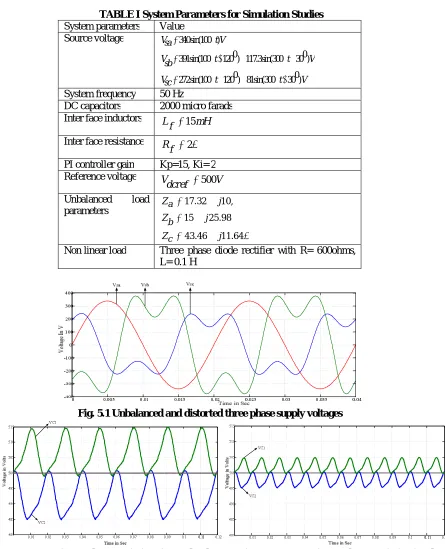
The system parameters for the simulation studies are given in Table 1.
TABLE I System Parameters for Simulation Studies
System parameters Value Source voltage 340sin(100 )
0 0
391sin(100 120 ) 117.3sin(300 30 )
0 0
272sin(100 120 ) 81sin(300 30 )
Vsa t V
V t t V
sb
Vsc t t V
System frequency 50 Hz
DC capacitors 2000 micro farads Inter face inductors L 15mH
f
Inter face resistance R 2
f
PI controller gain Kp=15, Ki= 2
Reference voltage V 500V
dcref
Unbalanced load parameters
17.32 10,
15 25.98
43.46 11.64
Za j
Z j
b
Zc j
Non linear load Three phase diode rectifier with R= 600ohms, L= 0.1 H
Fig. 5.1 Unbalanced and distorted three phase supply voltages
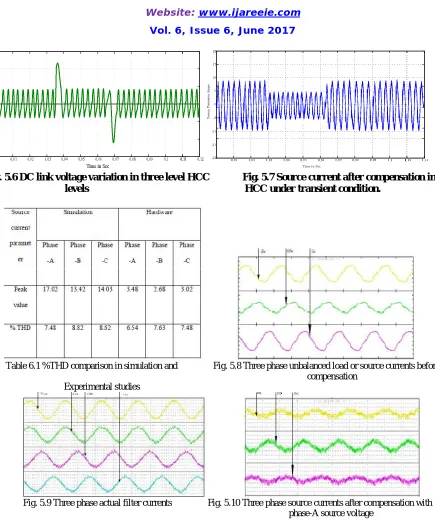
Fig. 5.2 DC Capacitors voltage variations in two level HC Fig. 5.3 DC Capacitors voltage variation in Three level HCC
this zero level switching, the variation of voltage across two capacitors is reduces which is shown in Fig. 5.3. The voltage variation across two capacitors in two level shown in Fig. 5.2. In this it is clearly shown that, under two level HCC voltage variations is more, whereas in three level voltages variation reduces considerably.
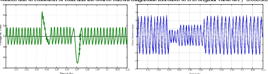
4.4 Transient performance of DC link Voltage controller in two levels HCC
The Eqn. (19) is used to generate DC load power including losses in the inverter. While maintaining this dc load power constant using PI controller under two level HCC, it is possible to maintain the capacitor voltage also constant. From the Fig. 5.4 it is observed that, initially the compensator is operated under steady state conditions. At
0.03 sec
t , load is suddenly reduced to half of it is original. Due to this sudden reduction of load, power consumed by
the load reduces and the capacitor absorbs surplus power supplied by the source. Because of this surplus power the capacitor voltages will increase above the reference value. Using PI controller gain the variation in the capacitor voltages will come back to it is reference value att0.045 sec. After few cycles att0.065 sec, the load switches back to it is full load. At this point of time, load requires high amount of power and this power will be supplied from the capacitors due to which the capacitor voltage will fall down. Again the PI controller action starts and brings the voltage variation in the capacitor to it is reference value within few cycles. From Fig. 5.5, it is observed that the source current changes with respect to the load and dc link voltage changes. Att0.03 sec, the source current magnitude reduces due to reduction of load and the source current magnitude increases to it is original value att 0.065 sec
Fig. 5.4 DC link voltage variation in two level HCC , Fig. 5.5 Source current after compensation in two levels HCC under transient condition.
5.2 Transient performance of DC link Voltage controller in three levels HCC
The Eqn. (19) is used to generate DC load power including losses in the inverter. While maintaining this dc load power constant using PI controller under three level HCC, it is possible to maintain the capacitor voltage also constant. From the Fig. 5.6 it is observed that, initially the compensator is operated under steady state conditions. At
0.03 sec
t , load is suddenly reduced to half of it is original. Due to sudden reduction of load, power consumed by the
Fig. 5.6 DC link voltage variation in three level HCC Fig. 5.7 Source current after compensation in three levels HCC under transient condition.
Table 6.1 %THD comparison in simulation and Fig. 5.8 Three phase unbalanced load or source currents before compensation
Experimental studies
Fig. 5.9 Three phase actual filter currents Fig. 5.10 Three phase source currents after compensation with phase-A source voltage
In Fig. 5.5 shows the unbalanced load or source currents before compensation due to unbalanced non liner load. After compensation the source current found unbalanced and distorted because of generation of compensator currents are not independent as shown in Fig. 5.6. The %THD variation shown in table 6.3 is found that the distortion is above the normal limits of IEEE standards.
VII. CONCLUSION
This paper presents a state space model for three phase four wire systems with non stiff source. A control algorithm has proposed to compensate AC and DC components under unbalanced non linear load conditions. Initially a fixed unbalanced load will be considered in three phases along with non linear load. It is observed that after compensation the source currents are balanced and in phase with source voltage. The source currents observed balanced even after increasing the load in all three phases. A three level hysteresis current controller has been used to generate switching commands for inverter switches.
BIOGRAPHY
K.Srinivas received the B.E. degree in electrical and electronics engineering from Chithanya Bharathi Institutue of Technology and Science, Hyderabad, Osmania University, Hyderabad, India, in 2002, the M.Tech. Degree in power systems and Power Electronics from the Indian Institute of Technology, Madras, Chennai, in 2005, pursuing Ph.D from Jawaharlal Nehru Technological University Hyderabad. Currently, he is an Assistant Professor in Electrical and Electronics Engineering Department, Jawaharlal Nehru Technological University Hyderabad College of Engineering Karimanagar. His fields of interest include power quality and power-electronics control in power systems.
REFERENCES
[1]. M. Bollen, Understanding Power Quality Problems: Voltage Sags andInterruptions. New York: IEEE Press, 1999.
[2]. Karuppanan P, Saswat Kumar Ram and KamalaKanta mahapatra “Three level Hysteresis current controller based Active power filter for harmonic compensation, Proceedings of ICETECT 2011, pp 407-412.
[3]. B. Singh, K. Al-Hadded and A. Chandra, “A review of active filters for power quality improvements,” IEEE Trans. Industrial Electronics, Vol. 46, No. 5, Oct. 1998, pp. 960-971.
[4]. Arindam Ghosh, SMIEEE and Avinash Joshi, “A new approach to load balancing and power factor correction in power distribution system”. IEEE
Transactions on power Delivery, 2000, pp 417-422.
[5]. K.srinivas, Dr S S Tulasi Ram” A Control Algorithm of Power Factor Correction for single phase shunt active power filter under distorted supply voltages/currents” IJAREIE, Vol. 3, Issue 2, February 2014.
[6]. K.srinivas, Dr S S Tulasi Ram” A Three Phase Four Wire Shunt Active Power Filter Control Algorithm” IJACR, Vol. 4, Issue 14, March 2014.
[7]. under Unbalanced and Distorted Supply Voltage
[8]. HIROFUMI AKAGI, YOSHIHIRA KANAZAWA, and AKIRA NABE, “Instantaneous Reactive Power Compensators Comprising Switching
Devises without Energy Storage Components.” IEEE Trans, Industry Applications, Vol. IA-20, No. 3, pp. 625-630, 1984.
[9]. Andrea Cavallini and Gian Carlo Montanari, “Compensation Strategies for Shunt Active-Filter Control.” IEEE Trans, On Power Electronics, Vol. 9,
NO. 6, November 1994.
[10]. Fag Zheng Peng, and Jih-Sheng Lai, “Generalized Instantaneous Reactive Power Theory for Three-Phase Power Systems.” IEEE Trans, On
Instrumentation and Measurement, Vol. 45, No. 1, February 1996.
[11]. Linash P. K. and Mahesh K. M., A control algorithm for single-phase active power filter under non-stiff voltage source, IEEE Trans. on Power Electronics, May 2006, Vol. 21, No. 3. pp. 822-825.
[12]. H. Akagi and R. Kondo, “A transformer less hybrid active filter using a three-level pulse width modulation (PWM) converter for a medium- voltage
motor drive,” IEEE Trans. Power Electron., vol. 25, no. 6, pp. 1365–1374, Jun. 2010.
[13]. A. Nabae, S. Ogasawara and H. Akagi, “A novel control scheme for current-controlled PWM inverters,” IEEE Trans. on Industrial Application, Vol.
IA-22, No. 4, Julu/Aug. 1986, pp. 697-701
[14]. Mahesh, K. M. and K. Karthikeyan (2006) A study on design and dynamics of voltage source inverter in current control mode to compensate unbalance and non-linear loads. Proceedings of IEEE International Conference on Power Electronics, Drives and Energy Systems for Industrial Growth, New Delhi, December, 1-8.
[15]. U. K. Rao, M. K. Mishra, and A. Ghosh, “Control strategies for load compensation using instantaneous symmetrical component theory under different
supply voltages,” IEEE Trans. Power Del., vol. 23, no. 4, pp. 2310–2317, Oct. 2008.
[16]. A. Sahoo and T. Thyagarajan, “Modeling of facts and custom powerdevices in distribution network to improve power quality,” in Proc. Int. Conf. Power Syst., 2009, pp. 1–7.
[17]. Arya, S.R. ; Singh, B.Generation, Transmission & Distribution, IET , Implementation of distribution static compensator for power quality enhancement using learning vector quantisation, Generation, Transmission & Distribution, IET , Jan 2014, Vol. 7, No. 11. pp. 1244- 1252.
[18]. Thanh Hai Nguyen ; Dong-Choon Lee ; Chan-Ki Kim , A Series-Connected Topology of a Diode Rectifier and a Voltage-Source Converter for an
HVDC Transmission System, IEEE Trans. on Power Electronics, Jan 2014, Vol. 29, No. 4. pp. 1579- 1584.
[19]. Mahesh K. Mishra and K. Karthikeyan. A three-phase DSTATCOM compensating ac and dc loads with fast dynamic response. IEEE Canadian