Available online: https://edupediapublications.org/journals/index.php/IJR/ P a g e | 370
IMPLEMENTATION OF HIGH SPEED SENSE
AMPLIFIER FOR 6 T SRAM WITH HIGHLY
CONFIGURABLE LOW-VOLTAGE WRITE-ABILITY
ASSIST METHOD
PUTHI YASWANTH KUMAR1, BALA KRISHNA2
1 P.G Student, VLSI DESIGN
2 Associate Professor, Department of Electronics and Communication Engineering, ELURU
COLLEGE OF ENGINEERING.
Abstract: The Sense amplifier’s sense delay is one important parameter to measure the speed of SRAM memory cell. The sense delay depends on the amplifier reaction time. This delay parameter is more vulnerable to device variations, temperature and supply voltage variations. A latch type voltage controlled sense amplifier considered among all the offered current and voltage sense amplifier types for data sensing from the SRAM cell. The modified conventional latch type voltage controlled coupling capacitor based sense amplifier is implemented to improve the performance of the memory cell. The proposed circuit scheme will provide the reasonable negative voltage at the sense amplifier virtual ground, then the driving capability of the pull down (NMOS) transistors is increased, hence it made the sense amplifier faster. The conventional sense amplifier is compared with proposed coupling capacitor sense amplifier. From the experimental results, it is observed that coupling capacitor based sense amplifier circuit scheme will decrease the sense amplifier reaction time and access the data fast. The result shows, the proposed scheme provides the improvement of sense delay reduction of 198ps at SS/-40 C/1.2v and 18ps at FF/127 C/1.2v process corners at the cost of power consumption
Key words: Coupling Capacitor SRAM cell Offset Reaction time
1.INTRODUCTION
The sense amplifier circuit is one part of SRAM In present day microprocessors are having more than consumption, fast data access, robust design and is now 50% of the chip size is used for cache memory. The design broadly used in portable devices [3-4] too. The sense of on-chip caches with faster and larger size continues to amplifier will play an important role during the memory be increasingly essential for high-speed processors. read operation. It is utilized to get the data from the Sense delay
Available online: https://edupediapublications.org/journals/index.php/IJR/ P a g e | 371 memory designs. As the technology energy
levels of the cell at read operation. Therefore the scaling increases continuously, it has become hard for on use of sense amplifier will provide the required voltage or chip memories to maintain the tendency of the delay current output logic levels and also improves the speed of reduction with the speed of present processors logic. The the memory. During the operation of the sense amplifier, cache memories are static random access memories the content of cell node data should not disturb. (SRAM). The larger memory design is built by the small However, due to the time variation of bit line charging and SRAM memory blocks [1]. But the structure of SRAM cell discharging and large capacitive loads, the design of the is fixed due to the limitation of technological level, so the high-speed sense
amplifier is most important for
highperformance improvement of the
SRAM mainly depends performance SRAM memory designs [6]. Optimum bit line on peripheral circuits [2]. differential voltage may play an important role, building bit line differential voltage takes a large time to discharge due to the huge bit line capacitance. Considering less differential voltage leads to speed up memory, but may cause a problem during the read operation, so optimal value should be taken.
2.SRAM Architecture
SRAM memory contains an array of SRAM cell (6T SRAM) and peripheral circuits. A typical The write driver circuit is used to write a data value to column of the SRAM array contains the following circuits the SRAM cell and it is directly connected to the bit lines. [7]: 6T SRAM cells, row and
column decoder circuits, The row and column decoder circuits are used to select a write driver, sense amplifier and pre-charge circuit as memory location which is to be read/write. The shown in Fig. 1. The SRAM cell is the main part of the functionality of the sense amplifier circuit is to amplify memory array, it is composed of two back to back small signals to full swing [8]. In the coming sections will connected inverters (N1-P1,N2-P2) with two access explain the classification of sense amplifiers with respect transistors (N3, N4) connected to paired bit-lines (BL, to their mode of operation and significance of their role in BLB) as shown in Fig. 2. Both N3 and N4 MOS transistors the SRAM read operation. are directly connected to the word line to perform the access write and read operations through the bit lines.
Fig. 1: Column circuit of SRAM Array
3. Write-Ability Assist Techniques
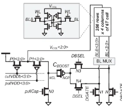
Fig.2 shows the implementation of the proposed write assist circuit. The design features a 4-to-1 column-multiplexing ratio such that four columns each having 256
memory cells interface with a BL
Available online: https://edupediapublications.org/journals/index.php/IJR/ P a g e | 372 inserted for every column of memory cells
to decouple VCOL from VDD during voltage collapse.
Fig. 2. Implementation of the proposed write-assist circuit
Another PMOS device (P1) is placed at every column between VCOL and the boost capacitor’s (CBOOST) left terminal (NCL) to charge CBOOST for negative BL operation. Pull-down device N0 is used to boost the charge across CBOOST to create a negative voltage at NCR node which is then transferred to BL or BLB of the selected column through two levels of multiplexing. The first level of multiplexing is done by NMOS devices N3 and N4 controlled by DSEL/DBSEL signals and the second level of multiplexing is done by BL MUX block to select the active column undergoing a write operation. Finally, N1 and N2 pull-down devices constitute the conventional write driver to discharge one of the BLs at the beginning of the write access depending on the polarity of input data. Although not
shown on the figure, cross-coupled PMOS keepers are placed between BL/BLB pairs of every column to keep the high BL at VDD during the write operation. To allow negative BL operation, DGATE/DGATEB signals are pulsed and both N1 and N2 are turned OFF before the application of negative BL operation. It should be noted that CBOOST and devices N0–N4 are shared across four columns of memory cells. The design in this work allows applying negative BL and VDD collapse write assists separately or at the same time.
4. CAPACITOR-BASED THRESHOLD MATCHING CIRCUIT FOR SENSE
AMPLIFIERS
Fig. 3 Sense-amplifier design using capacitors for input device threshold
matching.
Available online: https://edupediapublications.org/journals/index.php/IJR/ P a g e | 373 cross-coupled inverters are critical to
amplify the initial differential. After this amplifi- cation, PMOS devices of the cross-coupled inverters turn ON and further amplify the differential to rail-to-rail voltage levels. Sense-amplifier offset is mostly
affected by the threshold voltage
mismatches between the NMOS devices of the crosscoupled inverters [20]. In this work, we are using capacitors to measure and store the threshold voltage information of the critical input transistors and then use the
voltage across these capacitors to
compensate for the threshold mismatches. Fig. 5 shows the offset compensated sense-amplifier design. C0 and C1 are NMOS devices connected as capacitors at the source of input devices N0 and N1, respectively. When the sense amplifier is reset (pchgb = “0”), input/output nodes of the sense amplifier are precharged to VDD. During this time, the top terminals of capacitors (ct0 and ct1 in Fig. 11) are precharged to VDD − VT ,N0 and VDD − VT ,N1, respectively, where VT ,N0 and VT ,N1 are threshold voltages of N0 and N1. In other words, N0 and N1 charge C0 and C1 to the point where both N0 and N1 are on the verge of turning ON. This ensures that driving strength of N0 and N1 will be mainly determined by the input voltages at the gates of N0 and N1, not by their threshold voltages. Fig. 12 shows the waveforms of various signals during the operation of the sense amplifier. During the phase denoted by the letter A, read operation (by the assertion of WL signal) as well as the sense-amplifier offset compensation operation start. During this phase, the sense amplifier is in reset mode and ct0 and ct1 are charged to VDD − VT for both N0 and N1. Also during this time, a differential is
building between the BLs since WL is asserted. When column-select transistors are turned ON, this differential is passed to the input/output terminals of the sense amplifier. If the column-select transistors are turned ON before ct0 and ct1 reach VDD − VT , input differentials will affect the sampling of threshold voltages. To prevent this, column-select transistors are on-purposely turned ON later into the WL pulse and input differential is passed to the input of the sense amplifier after threshold information is stored on C0 and C1. It should be noted that, as ct0 and ct1 voltages reach VDD − VT , input transistors N0 and N1 go into subthreshold region of operation and current through these transistors get smaller. Consequently, at the end of Phase A, voltage of ct0 and ct1 will not be exactly VDD − VT ,N1 and VDD − VT ,N2, but they will be
close to these voltage levels and
Available online: https://edupediapublications.org/journals/index.php/IJR/ P a g e | 374 operation. Although not shown in Fig. 11, a
latch is connected to the input/output terminals of the sense amplifier and stores the sense-amplifier output until the next acces.
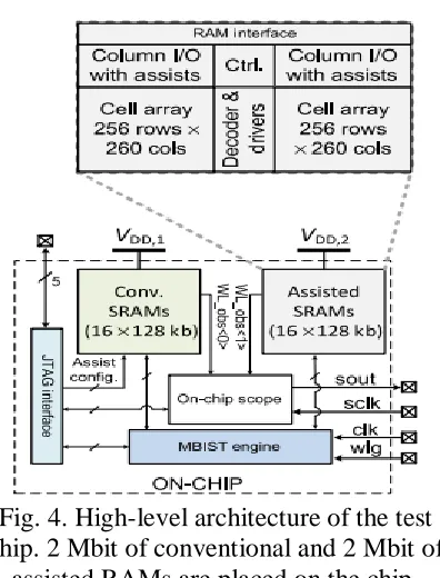
Configurable write-assist and
sense-amplifier offset compensation ideas are demonstrated on a test chip fabricated in a 28 nm HP CMOS process (Fig. 3). Fig. 4 shows the architecture of the test chip. On each die, 2 Mbits of conventional SRAMs are placed along with 2 Mbits of SRAMs featuring the write assist and sense-amplifier offset compensation ideas. SRAM bits are partitioned into 16 macros of 256 rows by 520 columns (including two redundant columns) for both conventional and assisted RAMs. Along with SRAM macros, an on-chip sampling scope, MBIST engine, and JTAG interface are also placed on the test chip. The on-chip sampling scope is used to monitor WL pulsewidths, while the MBIST engine creates various standard test patterns used for product testing. Finally, the JTAG
interface is used for off-chip
communication. SRAM macros on the test chip are designed to be phase based, where the low phase of the clock is used to assert the WLs.
Fig. 4. High-level architecture of the test chip. 2 Mbit of conventional and 2 Mbit of
assisted RAMs are placed on the chip.
In order to stress write-ability and read-ability problems without pushing operating frequency very high, an additional pin (wlg) is inserted for each macro that causes the WL pulse width to be shorter than the low phase of the clock. The on-chip sampling scope placed on the test chip is used to measure the WL pulsewidth observed on die by connecting it to one WL from the conventional and assisted SRAM macros.
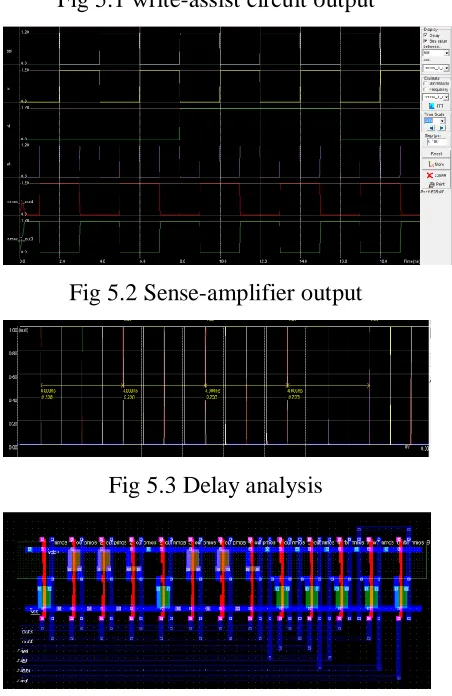
Available online: https://edupediapublications.org/journals/index.php/IJR/ P a g e | 375 Fig 5.1 write-assist circuit output
Fig 5.2 Sense-amplifier output
Fig 5.3 Delay analysis
Fig 5.4 Layout of proposed method
CONCLUSION
This paper presented a new design of coupling capacitor based sense amplifier for the improvement of sense amplifier reaction time in SRAM read operation. During the memory read operation the proposed circuit scheme provided the required negative voltage at the sense amplifier virtual ground, then the driving capability of the sense amplifier’s pull down NMOS transistors is increased, hence it reduces the reaction time and it made memory faster. The impact of
temperature on differential voltage is analysed and plotted the graph. The dependency of the sense amplifier reaction time on bit line differential voltage is observed. We compared the proposed circuit
scheme with conventional method,
therefore,the proposed scheme provides the improvement of delay reduction of 198ps at SS/-40 C/1.2v º and 18ps at FF/127 C/1.2v process corners at the cost of o power consumption of the SRAM cell in the read operation. The experimental results are measured across the PVT.
REFERENCES
[1] NVIDIA Corp.. (2015, Jan.). NVIDIA Tegra X1 White Paper [Online]. Available: http://international.download.nvidia.com/pdf /tegra/Tegra-X1- whitepaper-v1.0.pdf
[2] International Solid State Circuit
Conference. (2013, Nov. 1). ISSCC 2014
Tech Trends [Online]. Available:
http://isscc.org/doc/2014/2014_Trends. pdf [3] R. Kan et al., “The 10th generation 16-core SPARC64 processor for mission critical UNIX server,” IEEE J. Solid-State Circuits, vol. 49, no. 1, pp. 32–40, Jan. 2014.
[4] S. Rusu et al., “Ivytown: A 22 nm 15-core enterprise Xeon processor family,” in
IEEE Int. Solid-State Circuits Conf.
(ISSCC) Dig. Tech. Papers (ISSCC), Feb. 2014, pp. 102–103.
[5] P. Li et al., “A 20 nm 32-core 64 MB L3 cache SPARC M7 processor,” in IEEE Int. Solid-State Circuits Conf. (ISSCC) Dig. Tech. Papers (ISSCC), Feb. 2015, pp. 72– 73.
Available online: https://edupediapublications.org/journals/index.php/IJR/ P a g e | 376 [7] V. Gutnik and A. Chandrakasan,
“Embedded power supply for low-power DSP,” IEEE Trans. Very Large Scale Integr. (VLSI) Syst., vol. 5, no. 4, pp. 425–435, Dec. 1997.
[8] A. P. Chandrakasan et al., “Technologies for ultradynamic voltage scaling,” Proc. IEEE, vol. 98, no. 2, pp. 191–214, Feb. 2010.