OMNI-DIRECTION REFLECTION IN ONE DIMENSIONAL PHOTONIC CRYSTAL
R. Srivastava
Department of Physics
Udai Pratap Autonomous College Varanasi 221002, India
K. B. Thapa
Department of Physics
U.I. E.T, C. S. J. M. University Kanpur-208024, India
S. Pati
Department of Physics
Udai Pratap Autonomous College Varanasi 221002, India
S. P. Ojha
C. C. S. University Meerut 200005, India
1. INTRODUCTION
Over the past decades, much attention has been given to photonic crystals (PCs) as a new kind of optical materials [1–6]. These materials are based on the interaction between an optical field and materials exhibiting periodicity on the scale of wave length. The main feature of photonic crystals is that they can prohibit the propagation of electromagnetic waves within a certain frequency range called photonic band gap (PBG). The materials containing PBG have many potential applications in optoelectronics and optical communication. For the optical range within which the main application is expected, most of experimental effort has been concentrated on two dimensional and three dimensional photonic crystals. The application of two dimensional and three dimensional photonic crystals is limited. Complete two dimensional and three dimensional band gap can be realized in photonic crystals where the refractive index is periodically modulated in two- and three-dimension respectively [2, 6–10].
Besides two dimensional and three dimensional photonic crystals, the simplest periodic structure both in geometry and manipulating is a one dimensional stack of two types of layer which differs in the dielectric constants. One dimensional photonic crystal is attractive since their production is more feasible at any wavelength scale and their analytical and numerical calculations are simpler. It has been shown that one dimensional photonic crystals can totally reflect arbitrary polarized, transverse-electric (TE) and transverse-magnetic (TM), lights i.e., omnidirectional reflection, at all angles within the PBGs, can take place even in the absence of a complete band gap i.e., these crystals exhibit the property of omni-directional reflection [4, 6, 11].
Recently, several research groups worldwide have reported that a simple-to-fabricate periodic one dimensional medium can have high reflectivity over a wide range of frequencies at all incident angles, i.e., an omnidirectional reflection. The total reflection band that occurs in any direction for TEand TM polarization is called omni-directional reflector mirror. One dimensional photonic crystal designed as Bragg mirror. Mirrors are of two basic varieties, a metallic mirror or omni-directional reflector and a dielectric Bragg mirror. One dimensional photonic crystal is designed as Bragg mirror [12–20]. In particular, large parts of these one dimensional photonic crystals were designed for application in the infrared wavelength ranges. Several research groups have reported that a simpler to fabricate Bragg mirror suffices to design a low loss omni-directional reflector [21–29].
for incident light under certain conditions. They constructed a stack of nine alternating micrometer thick layers of Polystyrene and Tellurium and demonstrated omnidirectional reflection over the wavelength range from 10 to 15 micrometers. Gallas et al. [31] reported the annealing effect in the Si/SiO2 omni reflectors. Chen et al. [32] fabricated six
bilayers of SiO2 and TiO2 quarter wave films using the sol-gel method
and found an omnidirectional PBG of about 70 nm in near IR range. Chigrin et al. [6, 18] fabricated a lattice consisting of 19 layers of Na3AlF6 and ZnSe and found that omnidirectional photonic band gap
exists in the spectral range 604.3–638.4 nm. Lee and Yao [33] studied a wide range of realistic fabrication parameters for the formation of omnidirectional photonic band gaps (PBGs) in one-dimensional photonic crystals, theoretically as well as experimentally.
In this paper, the reflectivity of Na3AlF6/Ge multilayer structure
has large values of total omni-directional reflection than experimentally observed. The thicknesses of the each layer are taken 50% of the total thickness of the unit cell for low and high index of refractions respectively. Such Na3AlF6/Ge multilayer structure has large total
omni-directional reflection than experimentally observed values for same structure with 50% of total thickness of unit cell for each material.
2. THEORY
The Helmholtz equation for considered periodic structure (photonic crystal);
∇2E +ω2
c2εrµrE = 0 (1)
where ε(x)µ(x) = n2(x), with n(x) is the refractive index. We deled
with electromagnetic wave propagated in thex-direction and polarized linearly. We take the y-axis is the direction of the polarization. The electric field of the propagated wave is denoted by the complex function E(x, y) for convenience
E(x, y) =E(x)eiβy (2)
where E(x) = Ajeikjxx + Bje−ikjxx for nj = √εj, β = ωcnjsinθ, kjx = ωcnjcosθj, θj is the angle of incidence, Aj, Bj are coefficients of reflected and incidence wave respectively with j = 1, 2. The wave vectors of first and second medium are k1x and k2x respectively. The magnetic field vectorH can be obtained alongy-axis;
H= i
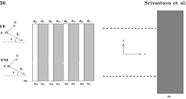
Figure 1. Schematic of the multilayer system with the incident wave vectork, the electromagnetic mode convention Eand B are the electric and magnetic fields, respectively.
A periodic arrangement of a multilayer film with refractive indices n1 and n2 and thickness d1 and d2 respectively is shown in Figure 1.
This structure is surrounded by the refractive indicesn0 andns, called incidence and substrate medium. The solution for Equation (1) will be superposition of plane waves traveling to the right and to the left. Say, for layer with indexn1, the right going and left going plane waves
have amplitudes A1 and B1 respectively and for layer with index n2
right going and left going planes waves have amplitudes C1 and D1
respectively. Hence for layer with indexn1 the solution of Equation (2)
is
E(x) =A1eik1xx+B1e−ik1xx (4)
and
E(x) =C1eik2x(x−d1)+D1e−ik2x(x−d1) (5)
for the layer with index n2. The parameterk1x and k2x will be called the wave number, and the definition is given by k1x = ωcn1cosθ1
and k2x = ωcn2cosθ2. At the interface between layers (x = d1), the
Equations (2) and (3) are continuous. This gives a relation between plane waves amplitude;
C1
D1
=M12
A1
B1
with
M12=
1 2
1 +k1x k2x
eik1xd1 1
2
1−k1x k2x
e−ik1xd1
1 2
1− k1x k2x
eik1xd1 1
2
1 +k1x k2x
e−ik1xd1
(7)
and also at x =d, the interface between layer with indexn2 and n1,
continuity of the Equations (2) and (3) which gives;
A2
B2
=M21
C1
D1
(8)
where the matrix M21 is the same as (7) but with interchanging the
indices. Using matrix Equations (7) and (8) and eliminating C1 and
D1, we found the matrix for binary structure;
A2
B2
=M21M12
A1 B1 (9a) or A2 B2
=Mi,j
A1
B1
(9b)
where Mi,j = M21M12. The matrix element of Mi,j is given
by; M1,1 = eik1xd1
cos(k2xd2) + 12i
γ+γ1
sin(k2xd2)
, M1,2 =
e−i k1xd1
+12i
1
γ −γ
sin(k2xd2)
, M2,1 = ¯M1,2, M2,2 = ¯M1,1, with
γ = k1x
k2x for TE-mode and γ= k1x×n22
k2x×n21
for TM-mode.
For the period of the lattices, E(x, K) = UK(x)eiK(ω)x with UK(x) is a complex valued periodic function of the lattices UK(x) = UK(x+d). The thickness of the unit cell is given as d(= d1 +d2). The parameter K(ω) is called the Bloch wave number or Dispersion Relation. There is an explicit expression forK(ω) as follows;
K(ω) = 1 dcos
−1
1
2T r[Mi,j]
(10)
withMi,j given in Equation (9). So Equation (10) becomes;
K(ω) = 1 dcos
−1[cos (k
1xd1)×cos (k2xd2)
−1 2
γ+ 1 γ
×sin (k1xd1)×sin (k2xd2)
Considering the structure of N period of layers with alternately refractive indices n1 and n2 and thickness d1 and d2, the coefficients
of propagating states in right and left side of the multilayer structures are calculated by multiplying transfer matrices of each cell.
A0
B0
= (Mi,j)1×(Mi,j)2×(Mi,j)3. . .(Mi,j)N
AN BN
(12)
The reflectance coefficient is given by,
rN =
B0
A0
BN=0
(13)
The reflectance is obtained by taking absolute value of the reflectance coefficient,
R= (|rN|)2 (14)
3. RESULTS AND DISCUSSION
For the sake of numerical calculation we take Na3AlF6/Ge dielectric
material with low and high index contrast. The refractive index for Na3AlF6 is n1 = 1.34 and for Ge is n2 = 4.2. Taking thickness of
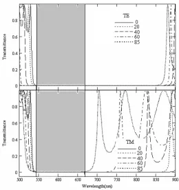
the each layer same a = b and d = a+b = 115 nm in the visible region. Applying transfer matrix method [34, 35] a graph is plotted between reflectance and wavelength. Figure 2 and Figure 3 shows the reflectivity of calculated spectra at different angle 0◦, 20◦, 40◦, 60◦ and 85◦ for TEand TM mode respectively and the ODR is found at 0◦ to 86◦ shown in Figure 4.
Table 1. For Na3AlF6/Ged= 115 nm and a=b).
Angle (deg) TE (nm) Band width TM (nm) Band width 0 540–894 354 540–894 354
20 535–891 356 539–871 332
40 522–883 361 535–810 271
60 508–874 366 533–733 200
85 500–868 368 536–670 134
ODR range . . . . 540–670 nm and ODR width. . . . 130 nm
Figure 2. Transmittance curve Vs wavelength (nm) of Na3AlF6/Ge
multilayer structure for TEmode at different angle.
Figure 3. Transmittance curve Vs wavelength (nm) of Na3AlF6/Ge
multilayer structure for TM mode at different angle.
Figure 4. Omnidirectional gap of Na3AlF6/Ge multilayer structure
for TEand TM mode at different angle.
4. CONCLUSION
In conclusion, we have shown theoretically that a one-dimensional dielectric structure can exhibit total omnidirectional reflection of incident light. Such a structure can be used as a very useful optical device in the optical industry. These findings should stimulate new experiments on controllable spontaneous emission of atoms, molecules and solid state micro-structures in the optical range [18].
REFERENCES
2. Jonopoulos, J. D., P. Villeneuve, and S. Fan, “Photonic crystals: Putting a new twist on light,”Nature, Vol. 386 143–149, 1997. 3. Zheng, Q. R., Y. Q. Fu, and N. C. Yuan, “Characteristics of planar
PBG structures with a cover layer,” Journal of Electromagnetic Waves and Applications, Vol. 20, 1439–1453, 2006.
4. Fink, Y., J. N. Winn, S. Fan, C. Chen, J. Michel, J. D. Joannopou-los, and E. L. Thomas, “A dielectric omnidirectional reflector,”
Science, Vol. 282, 1679–1682, 1998.
5. Rojas, J. A. M., J. Alpuente, J. Pi˜neiro, and R. S´anchez, “Rig-orous full vectorial analysis of electromagnetic wave propagation in 1D,”Progress In Electromagnetics Research, PIER 63, 89–105, 2006.
6. Chigrin, D. N., A. V. Lavrinenko, D. A. Yarotsky, and S. V. Gaponenko, “Observation of total omnidirectional reflection from a one-dimensional dielectric lattice,”Appl. Phys. A:Mater. Sci. Process., Vol. 68, 25–28, 1999.
7. Joannopoulos, J. D., R. D. Meade, and J. N. Winn, Photonic Crystals:Molding the Flow of Light, Princeton Univ. Press, Princeton, NJ, 1995.
8. Burstein, E. and C. Weisbuch, Confined Electron and Photon: New Physics and Applications, Plenum Press, New York, 1995. 9. Soukoulis, C., Photonic Band Gap Materials, 71–91, Kluwer
Academic, Dordrecht, 1996.
10. Knight, J. C., J. Broeng, T. A. Birks, and P. S. J. Russell,Science, Vol. 282, 1476, 1998.
11. Yablonovitch, E., “Photonic band-gap structures,” J. Opt. Soc. Amer. B, Vol. 10, 283–295, 1993.
12. Kurizki, G. and W. Hause, “Special issue on photonic crystals,”
Journal of Modern Optics, Vol. 41, 171–172, 1994.
13. Deopura, M., C. K. Ullal, B. Temelkuran, and Y. Fink, “Dielectric omnidirectional visible reflector,” Optics Letters, Vol. 26, 1197– 1199, 2001.
14. Almeida, R. and Z. Wang, “Sol-gel preparation of one-dimensional photonic bandgap structures,”Proc. SPIE, Vol. 4655, 24–33, 2002. 15. Russell, P. S. J., S. Tredwell, and P. J. Roberts, “Full photonic bandgapes and spontaneous emission control in 1D multilayer dielectric structures,”Opt. Commun., Vol. 160, 66–71, 1999. 16. Guida, G., “Numerical studies of disordered photonic crystals,”
Progress In Electromagnetics Research, PIER 41, 107–131, 2003. 17. Guenneu, S., A. Nicolet, F. Zolla, and S. Lasquellec, “Numerical
Electromagnetics Research, PIER 41, 271–305, 2003.
18. Chigrin, D. N., A. V. Lavrinenko, D. A. Yarotsky, and S. V. Gaponenko, “All dielectric one dimensional periodic structures for total omnidirectional reflection and partial spontaneous emission control,”J. Lightwave Tech., Vol. 17, 2018– 2024, 1999.
19. Lekner, J., “Omnidirectional reflection by multilayer dielectric mirrors,”J. Opt. A:Pure Appl. Opt., Vol. 2, 349–352, 2000. 20. Zandi, O., Z. Atlasbaf, and K. Forooraghi, “Flat multilayer
dielectric reflector antennas,” Progress In Electromagnetics Research, PIER 72, 1–19, 2007.
21. Dowling, J. P., “Mirror on the wall: You’re omnidirectional after all?”Science, Vol. 282, 1841–1843, 1998.
22. Yablonovitch, E., “Engineered omnidirectional external-reflectivity spectra from onedimensional layered interference filters,”Optics Letters, Vol. 23, 1648–1649, 1998.
23. Maka, T., D. N. Chigrin, S. G. Romanov, and C. M. Sotomayor Torres, “Three dimensional photonic crystals in the visible regime,” Progress In Electromagnetics Research, PIER 41, 307– 335, 2003.
24. Ozbay, E., B. Temelkuran, and M. Bayinder, “Microwave application of photonic crystals,” Progress In Electromagnetics Research, PIER 41, 185–209, 2003.
25. Aissaoui, M., J. Zaghdoudi, M. Kanzari, and B. Rezig, “Optical properties of the quasi-periodic one-dimensional generalized multilayer Fibonacci structures,” Progress In Electromagnetics Research, PIER 59, 69–83, 2006.
26. Zheng, Q. R., Y. Q. Fu, and N. C. Yuan, “Characteristics of planar PBG structures with a cover layer,” Journal of Electromagnetic Waves and Applications, Vol. 20, 1439–1453, 2006.
27. Srivastava, S. K. and S. P. Ojha, “Omnidirectional reflection bands in one-dimensional photonic crystals with left-handed materials,” Progress In Electromagnetics Research, PIER 68, 91– 111, 2007.
28. Srivastava, S. K. and S. P. Ojha, “Omnidirectional reflection bands in one-dimensional photonic crystal structure using fluorescence films,” Progress In Electromagnetics Research, PIER 74, 181–194, 2007.
29. Srivastava, R., S. Pati, and S. P. Ojha, “Enhancement of omnidirectional reflection in photonic crystal heterostructures,”
30. Winn, J. N., Y. Fink, S. Fan, and J. D. Joannopoulos, “Omnidirectional reflection from a one-dimensional photonic crystal,”Optics Letters, Vol. 23, 1573–1575, 1998.
31. Gallas, B., S. Fission, E. Charron, A. Brunet-Bruneau, R. Vuye, and J. Rivory, Appl. Opt., Vol. 40, 5056, 2001.
32. Chen, K. M., A. W. Sparks, H. C. Luan, D. R. Lim, K. Wada, and L. C. Kimerling, Appl. Phys. Lett., Vol. 75, 3805, 1999. 33. Lee, H.-Y. and T. Yao, “Design and evaluation of omnidirectional
onedimensional photonic crystals,” J. Appl. Phys., Vol. 93, 819– 830, 2003.
34. Yeh, P., Optical Waves in Layered Media, John Wiley & Sons, New York, 1988.